Table of Contents
Advertisement
Quick Links
Chipsmall Limited consists of a professional team with an average of over 10 year of expertise in the distribution
of electronic components. Based in Hongkong, we have already established firm and mutual-benefit business
relationships with customers from,Europe,America and south Asia,supplying obsolete and hard-to-find components
to meet their specific needs.
With the principle of "Quality Parts,Customers Priority,Honest Operation,and Considerate Service",our business
mainly focus on the distribution of electronic components. Line cards we deal with include
Microchip,ALPS,ROHM,Xilinx,Pulse,ON,Everlight and Freescale. Main products comprise
IC,Modules,Potentiometer,IC Socket,Relay,Connector.Our parts cover such applications as commercial,industrial,
and automotives areas.
We are looking forward to setting up business relationship with you and hope to provide you with the best service
and solution. Let us make a better world for our industry!
Contact us
Tel: +86-755-8981 8866 Fax: +86-755-8427 6832
Email & Skype: info@chipsmall.com Web: www.chipsmall.com
Address: A1208, Overseas Decoration Building, #122 Zhenhua RD., Futian, Shenzhen, China
Advertisement
Table of Contents

Subscribe to Our Youtube Channel
Related Manuals for Altera DE5-NET


Summary of Contents for Altera DE5-NET
- Page 1 Chipsmall Limited consists of a professional team with an average of over 10 year of expertise in the distribution of electronic components. Based in Hongkong, we have already established firm and mutual-benefit business relationships with customers from,Europe,America and south Asia,supplying obsolete and hard-to-find components to meet their specific needs.
- Page 2 DE5-Net User Manual www.terasic.com June 20, 2018...
-
Page 3: Table Of Contents
......................58 LASH ROGRAMMING WITH SERS ESIGN 4.4 R ..........................60 ESTORE ACTORY ETTINGS PROGRAMMABLE OSCILLATOR CHAPTER 5 ....................62 5.1 O ................................62 VERVIEW 5.2 S 570 E RTL ............................66 XAMPLE BY DE5-Net User Manual www.terasic.com June 20, 2018... - Page 4 – DDR3 ........................105 7.4 PCI EFERENCE ESIGN TRANSCEIVER VERIFICATION CHAPTER 8 ....................112 8.1 T ................................112 8.2 L ............................. 112 OOPBACK IXTURE 8.3 T ................................114 ESTING ADDITIONAL INFORMATION ........................... 116 DE5-Net User Manual www.terasic.com June 20, 2018...
-
Page 5: Chapter 1 Overview
The Stratix® V GX FPGA features integrated transceivers that transfer at a maximum of 12.5 Gbps, allowing the DE5-Net to be fully compliant with version 3.0 of the PCI Express standard, as well as allowing an ultra low-latency, straight connections to four external 10G SFP+ modules. Not relying on an external PHY will accelerate mainstream development of network applications enabling customers to deploy designs for a broad range of high-speed connectivity applications. -
Page 6: Key Features
The following hardware is implemented on the DE5-Net board: FPGA Altera Stratix® V GX FPGA (5SGXEA7N2F45C2) FPGA Configuration On-Board USB Blaster II or JTAG header for FPGA programming Fast passive parallel (FPPx32) configuration via MAX II CPLD and flash memory ... -
Page 7: Block Diagram
PCI Express full-height and 3/4-length F igure 1-1 shows the block diagram of the DE5-Net board. To provide maximum flexibility for the 9 4 H 9 4 H users, all key components are connected with the Stratix V GX FPGA device. Thus, users can configure the FPGA to implement any system design. - Page 8 Figure 1-1 Block diagram of the DE5-Net board Below is more detailed information regarding the blocks in Figure 1-1. Stratix V GX FPGA 5SGXEA7N2F45C2 622,000 logic elements (LEs) 50-Mbits embedded memory 48 transceivers (12.5Gbps) 512 18-bit x 18-bit multipliers ...
- Page 9 50MHz oscillator Programming PLL providing clock for 10G SFP+ transceiver Programming PLL providing clock for SATA or 1G SFP+ transceiver Four Serial ATA ports SATA 3.0 standard at 6Gbps signaling rate DE5-Net User Manual www.terasic.com June 20, 2018...
- Page 10 Support for PCIe Gen1/2/3 Edge connector for PC motherboard with x8 or x16 PCI Express slot Power Source PCI Express 6-pin DC 12V power PCI Express edge connector power DE5-Net User Manual www.terasic.com June 20, 2018...
-
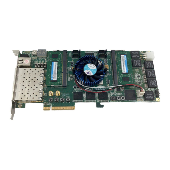
Page 11: Chapter 2 Board Components
This chapter introduces all the important components on the DE5-Net. Figure 2-1 is the top and bottom view of the DE5-Net development board. It depicts the layout of the board and indicates the location of the connectors and key components. Users can refer to this figure for relative location of the connectors and key components. -
Page 12: Configuration , Status And Setup
Launch Quartus Prime programmer and make sure the USB-Blaster II is detected. In Quartus Prime Programmer, add the configuration bit stream file (.sof), check the associated “Program/Configure” item, and click “Start” to start FPGA programming. DE5-Net User Manual www.terasic.com June 20, 2018... - Page 13 SW7.1 PCIE_PRSNT2n_x1 Off: Disable x1 presence detect On : Enable x4 presence detect SW7.2 PCIE_PRSNT2n_x4 Off: Disable x4 presence detect On : Enable x8 presence detect SW7.3 PCIE_PRSNT2n_x8 Off: Disable x8 presence detect DE5-Net User Manual www.terasic.com June 20, 2018...
- Page 14 Setting Position 2 of SW5 to high (right) specifies the default factory image to be loaded, as shown Figure 2-4. Setting Position 2 of SW5 to low (left) specifies the DE5-Net to load a user-defined image, as shown in Figure 2-5.
-
Page 15: General User Input /Output
Stratix V GX device pin numbers. Table 2-3 Push-button Pin Assignments, Schematic Signal Names, and Functions Board Schematic Stratix V GX Description Reference Signal Name Standard Pin Number DE5-Net User Manual www.terasic.com June 20, 2018... - Page 16 Table 2-4 Slide Switch Pin Assignments, Schematic Signal Names, and Functions Board Schematic Stratix V GX Description Reference Signal Name Standard Pin Number High logic level when SW in the UPPER 1.8-V PIN_B25 position. 1.8-V PIN_A25 1.8-V PIN_B23 DE5-Net User Manual www.terasic.com June 20, 2018...
- Page 17 Each segment in a display is identified by an index listed from 0 to 6 with the positions given in Figure 2-8. In addition, the decimal point is identified as DP. Table 2-6 shows the mapping of the FPGA pin assignments to the 7-segment displays. DE5-Net User Manual www.terasic.com June 20, 2018...
- Page 18 1.5-V PIN_G16 logic 1 on the I/O port turns the 7-segment signal HEX1 HEX1_D2 1.5-V PIN_F16 OFF. HEX1 HEX1_D3 1.5-V PIN_A7 HEX1 HEX1_D4 1.5-V PIN_B7 HEX1 HEX1_D5 1.5-V PIN_C9 HEX1 HEX1_D6 1.5-V PIN_D10 DE5-Net User Manual www.terasic.com June 20, 2018...
-
Page 19: Temperature Sensor And Fan Control
Negative pin of temperature diode in TEMPDIODEn 1.8-V PIN_P7 Stratix V TEMP_CLK SMBus clock 2.5-V PIN_D21 TEMP_DATAT SMBus data 2.5-V PIN_D20 TEMP_OVERT_n SMBus alert (interrupt) 2.5-V PIN_C22 TEMP_INT_n SMBus alert (interrupt) 2.5-V PIN_C21 FAN_CTRL Fan control 2.5-V PIN_AR32 DE5-Net User Manual www.terasic.com June 20, 2018... -
Page 20: Clock Circuit
SATA reference clocks respectively. The Si570 programmable clock generator is programmed via an I2C serial interface to generate the 10G Ethernet SFP+ reference clock. Two SMA connectors provide external clock input and clock output respectively. DE5-Net User Manual www.terasic.com June 20, 2018... - Page 21 PIN_AV34 Clock Output Defined SFP_REFCLK _p 100.0 MHz LVDS PIN_AK7 10G SFP+ SFP1G_REFCLK_p 125.0 MHz LVDS PIN_AH6 1G SFP+ SATA_HOST_REFCLK_p 125.0 MHz LVDS PIN_V6 SATA HOST SATA_DEVICE_REFCLK_p 125.0 MHz LVDS PIN_V39 SATA DEVICE DE5-Net User Manual www.terasic.com June 20, 2018...
-
Page 22: Rs-422 Serial Port
Figure 2-11 shows the RS-422 block diagram of the development board. The full-duplex LTC2855 is used to translate the RS-422 signal, and the RJ45 is used as an external connector for the RS-422 signal. DE5-Net User Manual www.terasic.com June 20, 2018... -
Page 23: Flash Memory
Internal Termination Resistance Enable. A high input will connect a RS422_TE PIN_AF16 termination resistor (120Ω typical) between pins A and B. The development board has two 1Gb CFI-compatible synchronous flash devices for non-volatile DE5-Net User Manual www.terasic.com June 20, 2018... - Page 24 Address bus 2.5-V PIN_AJ32 FSM_A6 Address bus 2.5-V PIN_AG33 FSM_A7 Address bus 2.5-V PIN_AL30 FSM_A8 Address bus 2.5-V PIN_AK33 FSM_A9 Address bus 2.5-V PIN_AJ33 FSM_A10 Address bus 2.5-V PIN_AN30 FSM_A11 Address bus 2.5-V PIN_AH33 DE5-Net User Manual www.terasic.com June 20, 2018...
- Page 25 Data bus 2.5-V PIN_AW32 FSM_D20 Data bus 2.5-V PIN_BD32 FSM_D21 Data bus 2.5-V PIN_AY31 FSM_D22 Data bus 2.5-V PIN_BA30 FSM_D23 Data bus 2.5-V PIN_BB30 FSM_D24 Data bus 2.5-V PIN_AM29 FSM_D25 Data bus 2.5-V PIN_AR29 DE5-Net User Manual www.terasic.com June 20, 2018...
-
Page 26: Ddr3 So-Dimm
Using differential DQS signaling for the DDR3 SDRAM interfaces, it is capable of running at up to 800MHz memory clock for a maximum theoretical bandwidth up to 95.4Gbps. Figure 2-13 shows the connections between the DDR3 SDRAM SO-DIMMs and Stratix V GX FPGA. DE5-Net User Manual www.terasic.com June 20, 2018...
Need help?
Do you have a question about the DE5-NET and is the answer not in the manual?
Questions and answers