
Related Manuals for Altera Max II


Summary of Contents for Altera Max II
- Page 1 MAX II Development Kit Getting Started User Guide 101 Innovation Drive San Jose, CA 95134 Development Kit Version: 1.1.0 (408) 544-7000 www.altera.com Document Version: 1.1.0 Document Date: July 2005 P25-10351-01...
- Page 2 Altera Corporation in the U.S. and other countries. All other product or service names are the property of their respective holders. Al- tera products are protected under numerous U.S.
-
Page 3: Table Of Contents
Reference Design 1: USB Reference Design ................2–16 Reference Design 2: The Slot Game Reference Design ............. 2–22 Reference Design 3: PCI Reference Design ................. 2–26 Altera Corporation Development Kit Version 1.1.0 July 2005 MAX II Development Kit Getting Started User Guide... - Page 4 Contents Development Kit Version 1.1.0 Altera Corporation MAX II Development Kit Getting Started User Guide July 2005...
-
Page 5: About This User Guide
First release of User Guide July 2005 1.1.0 Minor updates Refer to the readme file on the MAX II Development Kit CD-ROM for late-breaking information that is not available in this user guide. How to Contact ® For technical support or other information about Altera products, go to the Altera world-wide web site at www.altera.com. -
Page 6: Typographic Conventions
The angled arrow indicates you should press the Enter key. The feet direct you to more information on a particular topic. Development Kit Version 1.1.0 Altera Corporation MAX II Development Kit Getting Started User Guide July 2005... -
Page 7: Chapter 1. About This Kit
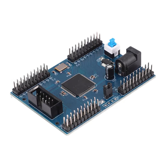
MAX II Development Board—The MAX II development board is a prototyping and evaluation platform that provides designers with an easy way to assess the features of the MAX II device and to begin building custom solutions with the MAX II device. Key features of the board include an EPM1270 device along with current sense circuitry, power-up time detection circuitry, SRAM, and an LCD. - Page 8 Features ■ Reference Designs/Demos—Altera provides several demos and reference designs with the MAX II Development Kit to help you get started building applications. See “Demo Designs” on page 2–7 “Reference Designs” on page 2–16 for more information on the designs provided.
-
Page 9: Chapter 2. Getting Started
There are several resistors that are unpopulated, as well as an EEPROM socket (J10). Refer to the MAX II EPM1270 Development Board Data Sheet (available on the MAX II Development Kit CD-ROM) for information on the board components and their locations. -
Page 10: Important Considerations
Installing the ® To install the MegaCore functions and reference designs, insert the MAX II Development Kit CD-ROM into your CD-ROM drive. Copy the MegaCore files to your hard drive. Function & The pci_t32 MegaCore function installer is available in the Reference <root>/Examples/HW/ReferenceDesigns/... -
Page 11: Installing The Quartus Ii Software
Figure 2–1. MAX II Directory Structure Installing the Refer to “Installing the Quartus II Software” in the Quartus II Installation & Licensing Manual for PCs, which is included on the MAX II Development Quartus II Kit CD-ROM, for the software installation instructions. After the software finishes installing, you must request and install a license to enable it. -
Page 12: Connecting The Cables And Power To The Board & Pc
MAX II device JTAG header on the board (J2) and connect the other end to your PC to configure the MAX II device directly using a POF file. Align the ByteBlaster II connector so that the red strip is orientated towards the Altera logo on the board. - Page 13 Memory—this is the non-volatile portion of the MAX II device that stores the configuration data and loads it into the logic portion of the MAX II device. The UFM refers to the User Flash Memory on the MAX II device. This is 8 Kbits of non-volatile user storage space.
-
Page 14: Running The Functional Test
MAX II Device” on page 2–4 for details on how to load POF files into the MAX II device.) The LCD should read “MAX II by Altera”. Push S2 to cycle through the tests. After pressing S2 once, the LCD screen should display the voltage of V . -
Page 15: Demo Designs
In order to allow users to investigate the fast power-up time of a MAX II device, the board is equipped with a circuit that allows users to observe the time it takes for a MAX II device to power up under a variety of different power supply loading conditions. - Page 16 MAX II device in accordance with the specifications given in the Data Sheet. Before performing a test to verify the power-up time of a MAX II device under a certain load, you should set the V supply to 2.5 V or 3.3 V,...
- Page 17 TCONFIG = 137us SW2 low = 000*TCfg TCONFIG refers to the time it takes the MAX II device to configure under the current loading conditions. SW2 low refers to the number of times the MAX II device could have configured itself in the time that the button was depressed.
- Page 18 Figure 2–4). Understanding the Results The most detailed analysis of the power-up character of a MAX II device comes from viewing probe points during the power-up cycle with a digital oscilloscope. The development board has a variable core V rise time control.
- Page 19 Getting Started V_INT shows the Core V rise time, and the rise time variation caused by POT1. ACTIVE_IO is driven by a MAX II user I/O pin that helps demonstrate the instant MAX II becomes functional (powered-up and configured). Figure 2–4 shows a typical digital oscilloscope output.
-
Page 20: Low Power Demonstration
CCINT Low Power Demonstration MAX II devices consume very little power, making them ideal for use in systems where power is at a premium. The MAX II development board is equipped with two current sense circuits that allow users to measure the power consumed by the MAX II device at different design densities and toggle rates. - Page 21 R95 and R99. Using the same technique as described for V allows CCINT you to calculate the total power being consumed by the MAX II device. This circuit uses resistors with a specified variance of 5%, which means that the power measurement is not precise. This circuit is provided to give users a general understanding of the MAX II device power consumption.
-
Page 22: Real-Time Isp Demonstration
(volatile) portion of the device. After a new POF file has been loaded into the MAX II device with real-time ISP enabled, cycling power causes the new design to become active in the MAX II device. Further power cycles simply reload the design residing in the CFM (you cannot switch back and forth between two different designs). - Page 23 Observe the Vending Machine Demo functioning as described below. Pressing S5 again results in the MAX II device reconfiguring itself with the Vending Machine Demo. The Functional Test design is now gone and would have to be reloaded into the CFM via the Quartus II programmer in order to be loaded into the MAX II device again.
-
Page 24: Reference Designs
It provides an example of the VHDL language for users new to programmable logic. Reference The MAX II Development Kit provides three reference designs to show how the MAX II board (and the MAX II device) can interface with other Designs systems. Reference Design 1: USB Reference Design... - Page 25 “Programming the MAX II Device” on page 2–4 for details on how to load POF files into the MAX II device.) To install the drivers, perform the following steps: When you plug the board into your PC, the message “Found New Hardware”...
- Page 26 COM4. This port number will be different on each machine. After you find which COM port your machine has assigned the MAX II board, select that port in the Current COM Port drop down box in the MAX II USB Utility user interface (see Figure 2–6).
- Page 27 MAX II board. Note the Default Encoding drop down box in the Control Options section of the user interface. This controls how the MAX II device interprets the data sent to and received from the MAX II board. If you select Hexadecimal, the PC will treat all data as hexadecimal characters.
- Page 28 SRAM. It contains the addresses and the data read from those addresses. SRAMDataBack.txt must not be open when you try to read from the SRAM. 2–20 Development Kit Version 1.1.0 Altera Corporation MAX II Development Kit Getting Started User Guide July 2005...
- Page 29 UFMInterface.v, the SRAMInterface.v, or the LCDInterface.v, depending on the value of the data received. Refer to the Verilog code itself for more details on the operation of this MAX II design. Altera Corporation Development Kit Version 1.1.0 2–21...
-
Page 30: Reference Design 2: The Slot Game Reference Design
The Visual Basic project consists of the GUI and various pieces of code that control the transmission and reception of data and control characters to and from the MAX II board. All data is interpreted based on which command buttons are pressed. After a command button is pressed, it is disabled until the PC receives data for the corresponding component. - Page 31 An LCD controller interprets the instructions provided by either path and supplies stimulus to the LCD hardware to render the appropriate images. See Figure 2–8. Altera Corporation Development Kit Version 1.1.0 2–23 July 2005 MAX II Development Kit Getting Started User Guide...
- Page 32 This block manages the status and functionality of the player controlled inputs Bet and Spin. The functionality of this block can be divided into three major areas: 2–24 Development Kit Version 1.1.0 Altera Corporation MAX II Development Kit Getting Started User Guide July 2005...
- Page 33 Bet signal to prepare for another spin. LCD Controller The MAX II Slot Game Reference Design communicates with the on-board LCD through a custom-built controller interface. The logic block performs several functions vital to the game behavior. Upon...
-
Page 34: Reference Design 3: Pci Reference Design
At any point during game play, pressing the Reset button (S5) will cycle the board power, stop the game, and reload the design’s programming file (.pof) into the SRAM (volatile) portion of the MAX II device via the Configuration Flash Memory. After the file has been reloaded, all registers are restored to their default value and the design returns to its initial introduction display. - Page 35 PCI_ReferenceDesign\Win2k_XP_Drivers\windrvr6.inf install r wdreg -inf <root>\Examples\HW\ReferenceDesigns\ PCI_ReferenceDesign\Win2k_XP_Drivers\ altera_maxiipci.inf install r Turn off your PC and install the MAX II development board in an available PCI slot. (Refer to your PC's hardware installation documentation.) Power-up the PC. Install the drivers: If you are using the Windows 2000 operating system, the operating system detects the MAX II development board as new hardware and prompts you to install a driver.
- Page 36 PC_Application directory. To demonstrate reading from and writing to the SRAM, perform the following steps: In the MAX II PCI application, choose the command to be Target Loop (default). Set the Address Offset to 0x0 (default). Change the number of bytes to 512.
- Page 37 A dialog box appears when an interrupt is received (see Figure 2–10). If multiple switches are pushed at the same time, multiple dialog boxes appear. Figure 2–10. Interrupt Received Dialog Box Altera Corporation Development Kit Version 1.1.0 2–29 July 2005 MAX II Development Kit Getting Started User Guide...
- Page 38 Reference Designs 2–30 Development Kit Version 1.1.0 Altera Corporation MAX II Development Kit Getting Started User Guide July 2005...
Need help?
Do you have a question about the Max II and is the answer not in the manual?
Questions and answers