
Subscribe to Our Youtube Channel
Related Manuals for Altera Stratix V GT


Summary of Contents for Altera Stratix V GT
- Page 1 Transceiver Signal Integrity Development Kit Stratix V GT Edition Reference Manual 101 Innovation Drive San Jose, CA 95134 www.altera.com MNL-01068-1.3 Feedback Subscribe Arrow.com. Downloaded from...
- Page 2 © 2016 Altera Corporation. All rights reserved. ALTERA, ARRIA, CYCLONE, HARDCOPY, MAX, MEGACORE, NIOS, QUARTUS and STRATIX words and logos are trademarks of Altera Corporation and registered in the U.S. Patent and Trademark Office and in other countries. All other words and logos identified as trademarks or service marks are the property of their respective holders as described at www.altera.com/common/legal.html.
-
Page 3: Table Of Contents
Featured Device: Stratix V GT FPGA ........ - Page 4 How to Contact Altera ........
-
Page 5: Chapter 1. Overview
FPGA designs that interface with all components of the board. General Description The Transceiver Signal Integrity Development Kit, Stratix V GT Edition, allows you to evaluate the performance of the Stratix V GT FPGA which is optimized for high-performance and high-bandwidth applications with integrated transceivers supporting backplane, chip-to-chip, and chip-to-module operation. - Page 6 Spread spectrum clock input ■ Four clock trigger outputs ■ ■ Transceiver interfaces Four 25.78-Gbps TX/RX channels to MMPX connectors (for Stratix V GT FPGA ■ only) Seven 12.5-Gbps TX/RX channels to SMA connectors ■ One 12.5-Gbps TX/RX channel to SFP+ cage ■...
- Page 7 ■ System Monitoring Temperature—FPGA die ■ Mechanical ■ 7.5" x 10.5" board dimension ■ January 2016 Altera Corporation Transceiver Signal Integrity Development Kit Stratix V GT Edition Reference Manual Arrow.com. Arrow.com. Arrow.com. Arrow.com. Arrow.com. Arrow.com. Arrow.com. Downloaded from Downloaded from...
-
Page 8: Development Board Block Diagram
Chapter 1: Overview Development Board Block Diagram Development Board Block Diagram Figure 1–1 shows the block diagram of the Stratix V GT transceiver signal integrity development board. Figure 1–1. Stratix V GT Transceiver Signal Integrity Development Board Block Diagram Buttons, Switches, Displays 16 Char ×... - Page 9 2. Board Components This chapter introduces all the important components on the Stratix V GT transceiver signal integrity development board. Figure 2–1 illustrates major component locations Table 2–1 provides a brief description of all features of the board. A complete set of schematics, a physical layout database, and GERBER files for the development board reside in the Stratix V GT development kit documents directory.
-
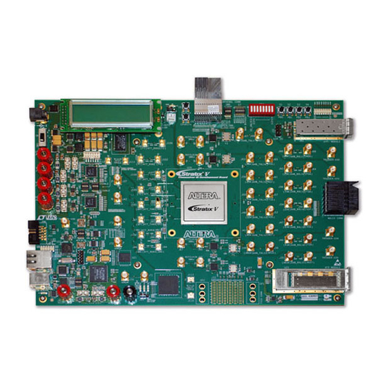
Page 10: Board Overview
Figure 2–1 provides an overview of the development board features. Figure 2–1. Overview of the Stratix V GT Transceiver Signal Integrity Development Board Features Amphenol Backplane Connector (J32) Reset Push Buttons (S5, S6) Fan Connector (J12) - Page 11 Ethernet LEDs Indicates the connection speed as well as transmit or receive activity. Clock Circuitry Feeds even-numbered REFCLKs on left side of the Stratix V GT device and trigger an output at board reference J81. The external input is Programmable oscillator available at board reference J79 and J80.
- Page 12 10Gbase-KR reference 7 transceiver-channel pairs, right angle receptacle for Amphenol backplane backplane connector. Transceiver Interfaces – Stratix V GT J94, J96, J98, Advanced transceiver interface Transceiver GTB receive channels connected to the MMPX connectors. J100, J102, J104, J106, J108...
- Page 13 Communication Ports RJ-45 connector which provides a 10/100/1000 Ethernet connection Gigabit Ethernet port through a Marvell 88E1111 PHY and the FPGA-based Altera Triple Speed Ethernet MAC MegaCore function in SGMII mode. Connects an Altera USB-Blaster dongle to program the FPGA and JTAG header MAX II CPLD devices.
-
Page 14: Featured Device: Stratix V Gt Fpga
Featured Device: Stratix V GT FPGA Featured Device: Stratix V GT FPGA The development board features the Stratix V GT 5SGTMC7K3F40C2 device (U29) in a 1517-pin FineLine BGA package. For more information about the Stratix V device family, refer to the Stratix V Device Handbook. - Page 15 Chapter 2: Board Components 2–7 Featured Device: Stratix V GT FPGA Table 2–4. Stratix V GT I/O Usage Summary (Part 2 of 3) Function I/O Type I/O Count Description Temperature Monitor Temperature sense diodes Analog Stratix V GT internal sense diode.
- Page 16 2–8 Chapter 2: Board Components Featured Device: Stratix V GT FPGA Table 2–4. Stratix V GT I/O Usage Summary (Part 3 of 3) Function I/O Type I/O Count Description 16 Character × 2 Line LCD 5.0-V LVTTL output Ethernet TXD[3:0] 2.5-V CMOS output...
-
Page 17: Max Ii Cpld System Controller
Chapter 2: Board Components 2–9 MAX II CPLD System Controller MAX II CPLD System Controller The board utilizes the EPM2210F256C3N System Controller, an Altera MAX II CPLD, for the following purposes: ■ FPGA configuration from flash memory ■ Temperature monitoring ■... - Page 18 Flash address bus F_AD20 AK12 2.5-V Flash address bus F_AD21 AK11 2.5-V Flash address bus F_AD22 Transceiver Signal Integrity Development Kit January 2016 Altera Corporation Stratix V GT Edition Reference Manual Arrow.com. Arrow.com. Arrow.com. Arrow.com. Arrow.com. Arrow.com. Arrow.com. Arrow.com. Arrow.com. Arrow.com. Arrow.com.
- Page 19 2.5-V Fast Passive Parallel (FPP) programming data in MAX_FPP_TDI — 2.5-V FPP programming data out MAX_FPP_TDO January 2016 Altera Corporation Transceiver Signal Integrity Development Kit Stratix V GT Edition Reference Manual Arrow.com. Arrow.com. Arrow.com. Arrow.com. Arrow.com. Arrow.com. Arrow.com. Arrow.com. Arrow.com.
- Page 20 PR_ERROR AD29 2.5-V FPGA partial reconfiguration ready PR_READY AE29 2.5-V FPGA partial reconfiguration request PR_REQUEST Transceiver Signal Integrity Development Kit January 2016 Altera Corporation Stratix V GT Edition Reference Manual Arrow.com. Arrow.com. Arrow.com. Arrow.com. Arrow.com. Arrow.com. Arrow.com. Arrow.com. Arrow.com. Arrow.com.
- Page 21 — 2.5-V USB configuration write to FIFO USB_MAX_WR — 2.5-V User image for configuration USER_IMAGE January 2016 Altera Corporation Transceiver Signal Integrity Development Kit Stratix V GT Edition Reference Manual Arrow.com. Arrow.com. Arrow.com. Arrow.com. Arrow.com. Arrow.com. Arrow.com. Arrow.com. Arrow.com. Arrow.com.
-
Page 22: Configuration, Status, And Setup Elements
FPGA Programming over Embedded USB-Blaster Programming the FPGA over embedded USB-Blaster is implemented using a type-B USB connector (CN1), a USB 2.0 PHY device, and an Altera MAX II CPLD EPM2210F256C3N (U19). This allows configuration of the FPGA using a USB cable that connects directly between the USB port on the board (CN1) and a USB port of a PC running the Quartus II software. -
Page 23: Fpga Programming From Flash Memory
FPP format. This 8-bit data is then written to the FPGA’s dedicated configuration pins during configuration. The FPP configuration is implemented with an Altera MAX II CPLD together with the Micron PC2800AP30BF 1-Gb CFI NOR-type flash device (U21). The CPLD shares the flash interface with the FPGA. - Page 24 Integrity Development Kit, Stratix V GT Edition User Guide. Flash Programming Flash programming is possible through a variety of methods using the Stratix V GT device. The first method is to use the factory design called the Board Update Portal. This design is an embedded webserver, which serves the Board Update Portal web page.
-
Page 25: Fpga Programming Over External Usb-Blaster
FPGA is the only device on the JTAG chain. JTAG Header The JTAG header provides another method for configuring the FPGA using an Altera USB-Blaster dongle with the Quartus II Programmer running on a PC. Figure 2–5 shows the schematic connections for the dedicated JTAG programming header (J93). -
Page 26: Status Elements
Driven by the Marvell 88E1111 PHY. Green LED. Illuminates to indicate Ethernet linked at 10 Mbps ENET_LED_LINK10 connection speed Driven by the Marvell 88E1111 PHY. Transceiver Signal Integrity Development Kit January 2016 Altera Corporation Stratix V GT Edition Reference Manual Arrow.com. Arrow.com. Arrow.com. Arrow.com. Arrow.com. -
Page 27: Setup Elements
ON : MAX II CPLD EPM2210 System Controller in-chain 6–7 MAX_BYPASS OFF : Bypass MAX II CPLD EPM2210 System Controller January 2016 Altera Corporation Transceiver Signal Integrity Development Kit Stratix V GT Edition Reference Manual Arrow.com. Arrow.com. Arrow.com. Arrow.com. Arrow.com. -
Page 28: Program Select Jumper
Manufacturer Board Reference Description Manufacturer Part Number Website Push Button Panasonic Corporation EVQPAC07K www.panasonic.com Transceiver Signal Integrity Development Kit January 2016 Altera Corporation Stratix V GT Edition Reference Manual Arrow.com. Arrow.com. Arrow.com. Arrow.com. Arrow.com. Arrow.com. Arrow.com. Arrow.com. Arrow.com. Arrow.com. Arrow.com. -
Page 29: Clock Circuitry
Figure 2–6 shows the default frequencies of all external clocks going to the Stratix V GT transceiver signal integrity development board. Figure 2–6. Transceiver Signal Integrity Development Kit Dedicated Transceiver Clocks Stratix V GT FPGA... -
Page 30: General-Purpose Clocks
An external differential clock source from SMA at CLK10p/n (J70/J71). ■ Figure 2–7 shows the general purpose clocks going in to the Stratix V GT transceiver signal integrity development board. Figure 2–7. Transceiver Signal Integrity Development Kit General Purpose Clocks... -
Page 31: Embedded Usb-Blaster Clocks
XFP cages, and SMA connectors. One 12.5-Gbps channel on the 28 Gbps side of the device is a dedicated CMU clock input from the SMA connectors. For the Stratix V GT device, the four 25.78-Gbps ATT channels connects to the MMPX connectors. - Page 32 Length match between this TX pair 2-12.5-Gbps RX to Molex connector (right side of transceiver block) Length match between this RX pair Transceiver Signal Integrity Development Kit January 2016 Altera Corporation Stratix V GT Edition Reference Manual Arrow.com. Arrow.com. Arrow.com. Arrow.com.
-
Page 33: Backplane Connectors
1.4-V PCML GXB receive GXBRXLN_21 1.4-V PCML GXB receive GXBRXLP_21 1.4-V PCML GXB receive GXBRXLN_22 January 2016 Altera Corporation Transceiver Signal Integrity Development Kit Stratix V GT Edition Reference Manual Arrow.com. Arrow.com. Arrow.com. Arrow.com. Arrow.com. Arrow.com. Arrow.com. Arrow.com. Arrow.com. Arrow.com. - Page 34 AJ36 GXB receive GXBRXLP_4 1.4-V PCML GXB receive GXBRXRN_0 1.4-V PCML GXB receive GXBRXRN_5 Transceiver Signal Integrity Development Kit January 2016 Altera Corporation Stratix V GT Edition Reference Manual Arrow.com. Arrow.com. Arrow.com. Arrow.com. Arrow.com. Arrow.com. Arrow.com. Arrow.com. Arrow.com. Arrow.com. Arrow.com.
- Page 35 1.4-V PCML GXB receive GXBRXRN_11 1.4-V PCML GXB receive GXBRXRP_6 1.4-V PCML GXB receive GXBRXRP_11 January 2016 Altera Corporation Transceiver Signal Integrity Development Kit Stratix V GT Edition Reference Manual Arrow.com. Arrow.com. Arrow.com. Arrow.com. Arrow.com. Arrow.com. Arrow.com. Arrow.com. Arrow.com. Arrow.com.
-
Page 36: General User Input/Output
The development board includes four user-defined push buttons that allow you to interact with the Stratix V GT device. When you press and hold down the push button, the device pin is set to logic 0; when you release the push button, the device pin is set to logic 1. -
Page 37: User-Defined Dip Switch
D25 are user LEDs that allow status and debugging signals to be driven to the LEDs from the designs loaded into the Stratix V GT device. The LEDs illuminate when a logic 0 is driven, and turns off when a logic 1 is driven. There is no board-specific function for these LEDs. -
Page 38: Character Lcd
Table 2–28 summarizes the LCD pin assignments. The signal names and directions are relative to the Stratix V GT device. Table 2–28. LCD Pin Assignments, Schematic Signal Names, and Functions Board Reference Stratix V GT Device... - Page 39 2×7 pin, 100 mil, vertical header Samtec TSM-107-01-G-DV www.samtec.com 2×16 character display, 5×8 dot Lumex Inc. LCM-S01602DSR/C www.lumex.com matrix January 2016 Altera Corporation Transceiver Signal Integrity Development Kit Stratix V GT Edition Reference Manual Arrow.com. Arrow.com. Arrow.com. Arrow.com. Arrow.com. Arrow.com. Arrow.com. Arrow.com. Arrow.com. Arrow.com.
-
Page 40: Components And Interfaces
The device is an auto-negotiating Ethernet PHY with an SGMII interface to the FPGA. The Stratix V GT device can communicate with the LVDS interfaces at up to 1.25 Gbps. The MAC function must be provided in the FPGA for typical networking applications. - Page 41 Board Reference Description Manufacturer Part Number Website Marvel Ethernet PHY BASE-T device 88E1111-B2-CAAIC000 www.marvell.com Semiconductor January 2016 Altera Corporation Transceiver Signal Integrity Development Kit Stratix V GT Edition Reference Manual Arrow.com. Arrow.com. Arrow.com. Arrow.com. Arrow.com. Arrow.com. Arrow.com. Arrow.com. Arrow.com. Arrow.com. Arrow.com.
-
Page 42: Transceiver Interfaces
Tyco www.amphenol.com Amphenol www.te.com XFP cage without light pipe, press fit 1489951-1 Tyco Transceiver Signal Integrity Development Kit January 2016 Altera Corporation Stratix V GT Edition Reference Manual Arrow.com. Arrow.com. Arrow.com. Arrow.com. Arrow.com. Arrow.com. Arrow.com. Arrow.com. Arrow.com. -
Page 43: Sfp+ Interface
SFP+ Interface Table 2–31 lists the pin assignments for the SFP+ interface (SFPA) and their corresponding schematic signal names and Stratix V GT pin numbers. Table 2–35. SFP+ Interface Pin Assignments, Signal Names and Functions Board Reference Stratix V GT... -
Page 44: Flash Memory
Table 2–37 lists the flash pin assignments, signal names, and functions. The signal names and types are relative to the Stratix V GT device in terms of I/O setting and direction. Table 2–37. Flash Pin Assignments, Schematic Signal Names, and Functions (Part 1 of 2) -
Page 45: Power Supply
An on-board multi-channel power monitor device (LTC2978) measures both the voltage and current for several specific board rails. This device has the capability to trim voltage outputs ±10%. January 2016 Altera Corporation Transceiver Signal Integrity Development Kit Stratix V GT Edition Reference Manual Arrow.com. Arrow.com. Arrow.com. Arrow.com. - Page 46 T85A23157 dual analog switch — Character LCD — LEDs (x13) — 2p5V Board power LED — Transceiver Signal Integrity Development Kit January 2016 Altera Corporation Stratix V GT Edition Reference Manual Arrow.com. Arrow.com. Arrow.com. Arrow.com. Arrow.com. Arrow.com. Arrow.com. Arrow.com. Arrow.com. Arrow.com.
-
Page 47: Power Measurement
SW2. The work around to this issue is to set switch SW2 in the close position at power up. January 2016 Altera Corporation Transceiver Signal Integrity Development Kit Stratix V GT Edition Reference Manual Arrow.com. Arrow.com. Arrow.com. Arrow.com. -
Page 48: Power Distribution System
VCCL_GTB Stratix V GT FPGA Power LDO (1.5 A) Other Power LTC3026 Ethernet LDO (1.5 A) Transceiver Signal Integrity Development Kit January 2016 Altera Corporation Stratix V GT Edition Reference Manual Arrow.com. Arrow.com. Arrow.com. Arrow.com. Arrow.com. Arrow.com. Arrow.com. Arrow.com. Arrow.com. -
Page 49: Temperature Sense
The Stratix V GT die uses a MAX1619 temperature sense device for temperature monitoring. The device connects to the MAX II CPLD EPM2210 System Controller and the Stratix V GT device by a 2-wire SMB interface. The MAX1619 device is located at slave address 0011000b (18h). -
Page 50: Statement Of China-Rohs Compliance
(2) X* indicates that the concentration of the hazardous substance of at least one of all homogeneous materials in the parts is above the relevant threshold of the SJ/T11363-2006 standard, but it is exempted by EU RoHS. Transceiver Signal Integrity Development Kit January 2016 Altera Corporation Stratix V GT Edition Reference Manual Arrow.com. Arrow.com. Arrow.com. -
Page 51: Additional Information
Additional Information This chapter provides additional information about the document and Altera. Board Revision History The following table lists the versions of all releases of the Stratix V GT transceiver signal integrity development board. Date Version Changes December 2015 Production silicon New device part number—5SGTMC7K3F40C2. - Page 52 Email Subscription Management Center page of the Altera website, where you can sign up to receive update notifications for Altera documents. The feedback icon allows you to submit feedback to Altera about the document. Methods for collecting feedback vary as appropriate for each document.
Need help?
Do you have a question about the Stratix V GT and is the answer not in the manual?
Questions and answers