
Related Manuals for Intel Stratix 10 GX


Summary of Contents for Intel Stratix 10 GX
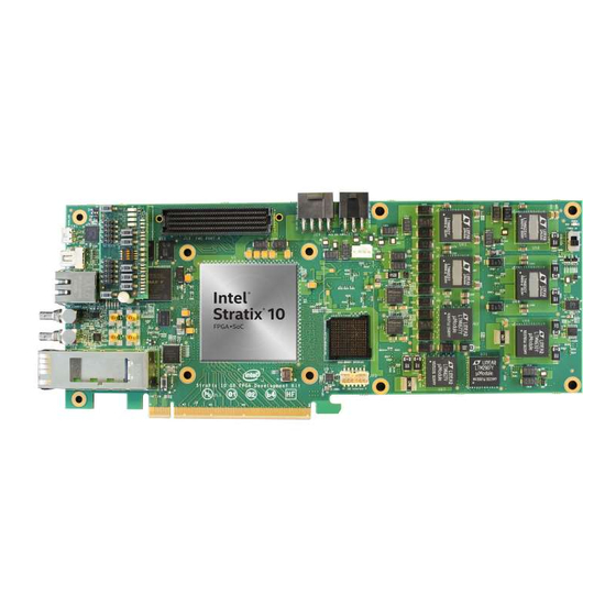
- Page 1 ® ® Intel Stratix 10 GX Transceiver Signal Integrity Development Kit User Guide UG-20047 2017.10.11 Subscribe Send Feedback...
-
Page 2: Table Of Contents
2 Getting Started........................ 5 2.1 Installing the Quartus Prime software................5 2.2 Installing the Development Board................5 2.3 Installing the Intel FPGA Download Cable Driver............6 3 Development Board Setup....................7 3.1 Setting up the Development Board................7 3.2 Factory Default Switch and Jumper Settings............... 8 4 Board Components......................11... - Page 3 A.1 Safety and Regulatory Information................87 A.1.1 Safety Warnings..................88 A.1.2 Safety Cautions..................89 A.2 Compliance and Conformity Information..............91 B Revision History......................92 B.1 User Guide Revision History................... 92 ® ® Intel Stratix 10 GX Transceiver Signal Integrity Development Kit User Guide...
-
Page 4: Overview
Intel's standard warranty, but reserves the right to make changes to any products and services Registered at any time without notice. Intel assumes no responsibility or liability arising out of the application or use of any information, product, or service described herein except as expressly agreed to in writing by Intel. Intel customers are advised to obtain the latest version of device specifications before relying on any published information and before placing orders for products or services. -
Page 5: Getting Started
Intel's standard warranty, but reserves the right to make changes to any products and services Registered at any time without notice. Intel assumes no responsibility or liability arising out of the application or use of any information, product, or service described herein except as expressly agreed to in writing by Intel. Intel customers are advised to obtain the latest version of device specifications before relying on any published information and before placing orders for products or services. -
Page 6: Installing The Intel Fpga Download Cable Driver
Intel FPGA Download Cable circuits for FPGA and MAX V programming. However, for the host computer and board to communicate, you must install the Intel FPGA Download Cable driver on the host computer. Installation instructions for the Intel FPGA Download Cable driver for your operating system are available on the Intel website. -
Page 7: Development Board Setup
Intel's standard warranty, but reserves the right to make changes to any products and services Registered at any time without notice. Intel assumes no responsibility or liability arising out of the application or use of any information, product, or service described herein except as expressly agreed to in writing by Intel. Intel customers are advised to obtain the latest version of device specifications before relying on any published information and before placing orders for products or services. -
Page 8: Factory Default Switch And Jumper Settings
Intel Stratix 10 GX FPGA device is configured successfully. If the configuration fails, the LED D23 ( ) illuminates. ERROR 3.2 Factory Default Switch and Jumper Settings This section shows the factory switch settings for the Intel Stratix 10 GX transceiver signal integrity development kit. Table 2. Factory Default Switch Settings Switch... - Page 9 SW9-3 OPEN/OFF Enable on-board VCCERAM VCCERAM regulator SW9-4 OPEN/OFF Enable on-board regulator SW8-1 OPEN/OFF Power Intel MAX 10 user DIP MAX10_DIPSWITCH Switch SW8-2 OPEN/OFF FAN is not full speed FAN_ON SW8-3 OPEN/OFF Select Linear Tech PWR PWR_MGMT_SEL MGMT solution SW8-4...
- Page 10 FMC + A FMC + B MXP-2 J50 SFP + 1 SFP + 0 S10GX MXP-1 J44 UF50 QSFP 28 1 MXP-0 J33 QSFP 28 0 CFP4 ® ® Intel Stratix 10 GX Transceiver Signal Integrity Development Kit User Guide...
-
Page 11: Board Components
Intel's standard warranty, but reserves the right to make changes to any products and services Registered at any time without notice. Intel assumes no responsibility or liability arising out of the application or use of any information, product, or service described herein except as expressly agreed to in writing by Intel. Intel customers are advised to obtain the latest version of device specifications before relying on any published information and before placing orders for products or services. - Page 12 4 Board Components Intel Stratix 10 GX Transceiver Signal Integrity Development Board Components Table 3. Board Components Table Board Reference Type Description Featured Devices FPGA Intel Stratix 10 GX 280 F2397 FPGA CPLD System MAX V CPLD (5M2210ZF256) FPGA USB Intel MAX 10 FPGA...
- Page 13 Type Description Feeds s on right side of the REFCLK Intel Stratix 10 GX FPGA device and an LVDS trigger output at board reference J8/J9. The external input is available at board reference J6 and J7. The default frequency is 706.25 MHz.
-
Page 14: Stratix 10 Gx Fpga
LTM4630A Power regulators for rail 3.3V 4.2 Stratix 10 GX FPGA The development board features the Intel Stratix 10 GX FPGA (1SG280UF50). Intel Stratix 10 GX FPGA I/O Usage Summary Table 4. Stratix 10 GX FPGA Pin Table Signal Name/Function... - Page 15 SFP+ 1 Management Data Clock SFP1_SCL SFP+ 1 Management Data I/O Bi- SFP1_SDA Directional Data CFP4 Module Low Power Mode CFP4_MOD_LOPWR CFP4 Module Reset CFP4_MOD_RSTn CFP4 Program Alarm bits CFP4_GLB_ALRMN continued... ® ® Intel Stratix 10 GX Transceiver Signal Integrity Development Kit User Guide...
- Page 16 FMC A clock direction control FACLKBIR1V8 FMC B LA bank GPIOs FBLAp/n[33:0] FMC B I C bus EXTB_SDA1V8 FMC I C bus EXTB_SCL1V8 FMC B present indicator FBPRSTN1V8_N continued... ® ® Intel Stratix 10 GX Transceiver Signal Integrity Development Kit User Guide...
- Page 17 Chip Select MAX5_CSn Write Enable MAX5_WEn Clock MAX5_CLK Byte Enable MAX5_BEn[3:0] Switches, Buttons, LED Light Emitting Diodes USER_LED[7:0] Push Buttons USER_PB[7:0] DIP Switches USER_DIP[6:0] Input/Output USER_IO[9:0] continued... ® ® Intel Stratix 10 GX Transceiver Signal Integrity Development Kit User Guide...
- Page 18 Reset ENET_RSTn Interrupt ENET_INTn Ethernet Management Data I/O ENET_MDIO Ethernet Management Data Clock ENET_MDC Other Bus Spare bus between Intel Stratix 10 and SPARE[20:1] MAX V Intel Stratix 10 I C bus I2C_1V8_SCL Intel Stratix 10 I C bus I2C_1V8_SDA...
- Page 19 CLK_MXP3_706M_p/n REFCLK transceiver bank 4F Differential bottom input to the CLK_GXB4F_644M_p/n REFCLK transceiver bank 4F Differential top input to the FAGBTCLKM2_Cp/n0 REFCLK transceiver bank 4K continued... ® ® Intel Stratix 10 GX Transceiver Signal Integrity Development Kit User Guide...
-
Page 20: Max V Cpld System Controller
4N 4.3 MAX V CPLD System Controller The Intel Stratix 10 GX transceiver signal integrity development kit consists of a MAX V CPLD (5M2210Z-F256), 256-pin FineLine BGA package. MAX V CPLD devices provide programmable solutions for applications such as FPGA reconfiguration from flash... - Page 21 SI5341 1 interrupt indicators SI5341_1_INTn SI5341 1 reset SI5341_1_RSTn SI5341 1 loss of clock indicators SI5341_1_LOLn SI5341 2 ENABLE SI5341_2_ENn SI5341 2 interrupt indicators SI5341_2_INTn SI5341 2 reset SI5341_2_RSTn continued... ® ® Intel Stratix 10 GX Transceiver Signal Integrity Development Kit User Guide...
- Page 22 Intel Stratix 10 configuration active indicator LED MAXV_LOAD Intel Stratix 10 configuration done indicator LED MAXV_CONF_DONE Intel Stratix 10 and MAX V data path, byte enable MAX5_BE_n[3:0] Intel Stratix 10 and MAX V data path, output enable MAX5_OEn Intel Stratix 10 and MAX V data path, chip select...
-
Page 23: Fpga Configuration
This section describes the FPGA, flash memory and MAX V CPLD System Controller device programming methods supported by the Intel Stratix 10 GX tranceiver signal integrity development kit. Three configuration methods except AS mode are mostly used on the Intel Stratix 10 transceiver signal integrity development kit. •... -
Page 24: Fpga Programming From Flash Memory
GX FPGA device is implemented using a Type-B USB connector, a CY7C68013A USB2 PHY device, and an Intel Intel MAX 10 10M04SCU169 FPGA. This will allow configuration of the Intel Stratix 10 GX FPGA device using a USB cable directly connected to a computer running Intel Quartus Prime software without requiring the external USB-Blaster dongle. - Page 25 MAX V CPLD. The PFL II Megafunction reads data from the flash and converts it to AvST format. This data is written into the Intel Stratix 10 GX FPGA device through dedicated AvST CLK and FPGA Config Data [31:0] pins at corresponding clock rate, such as 25 MHz, 50 MHz and 100 MHz.
-
Page 26: Fpga Programming Over External Usb-Blaster
MAX V CPLD. The on-board blaster JTAG chain connects four JTAG nodes in the following order, with the option to bypass the Intel Stratix 10, MAX V, FMC A or FMC B by a dip switch SW3 setting as follows: •... -
Page 27: Status Elements
4 Board Components Figure 7. JTAG Chain USB_MAX_TCK S10_JTAG_TCK USB_MAX_TDO USB-PHY S10_JTAG_TDO Intel USB_MAX_TMS Stratix 10 S10_JTAG_TMS USB_MAX_TDI S10_JTAG_TDI M5_JTAG_TCK M5_JTAG_TDO MAX V M5_JTAG_TMS BLASTER_DISn M5_JTAG_TDI External USB MAX 10 FPGA EXT_JTAG_TCK FATCK JTAG EXT_JTAG_TDO FATDO Header FMC-A EXT_JTAG_TMS FATMS... -
Page 28: Setup Elements
CPU Reset pushbutton JTAG Chain Device Removal Switch The JTAG chain connects the Intel Stratix 10 GX FPGA, the MAX V CPLD, FMC A and FMC B in a chain, with the option to selectively bypass each JTAG node by four dip switch setting. -
Page 29: User Input-Output Components
The development kit includes 8 user-defined pushbuttons and 4 system pushbuttons that allow you to interact with the Intel Stratix 10 GX FPGA. When you press and hold down the pushbutton, the device pin is set to logic 0; when you release the pushbutton, the device pin is set to logic 1. -
Page 30: User-Defined Dip Switch
D19 are user LEDs that allow status and debugging signals to be driven to the LEDs from the designs loaded into the Intel Stratix 10 GX FPGA device. The LEDs illuminate when a logic 0 is driven and turns off when a logic 1 is driven. There is no board- specific function for these LEDs. -
Page 31: Character Lcd
USER_LED7 4.7.4 Character LCD A 16 character x 2 line LCD display is connected to the Intel Stratix 10 GX FPGA device to display board information and IP address. The LCD module used is New Haven - NHD-0216K3Z-NSW-BBW-V3. This LCD module will be mounted to the Intel Stratix 10 GX transceiver signal integrity development board using a 1x10 vertical male 0.1"... -
Page 32: General-Purpose Clocks
REFCLK_GXB4C • J71/J72 SMA connectors direct connection to block REFCLK_GXB4K The figure below shows the dedicated transceiver clocks that are implemented on the Intel Stratix 10 GX FPGA development kit. Figure 8. Transceiver Dedicated Clocks Stratix 10 GX FAGBTCLKM2Cp/n3 (FMCA) - Page 33 4 Board Components • 50 MHz oscillator through an SL18860 buffer for Nios II applications. drives from on-board Intel FPGA Download Cable circuit. USB_FPGA_CLK • 25 MHz crystal supplied to an ICS557-03 Spread Spectrum differential clock buffer. The available frequencies and down spread percentages available from the spread spectrum buffer as shown in the table below.
-
Page 34: Embedded Usb-Blaster Clock
Cypress CY7C68013A USB2 PHY device. 4.9 Transceiver Channels The Intel Stratix 10 GX transceiver signal integrity development kit dedicates 78 channels from both the left and right sides of the device. Transceiver channels are allocated as shown in the table below. - Page 35 4 Board Components Figure 10. Stratix 10 GX FPGA Transceiver Usage Block Diagram Stratix 10 GX TX/RX (X16) FMC+ B TX/RX (X24) FMC+ A TX/RX (X1) SFP+ 1 TX/RX (X1) SFP+ 0 TX/RX (X6) External TX/RX (X4) Loopback MXP 2...
- Page 36 TXN1 TXP1 TXN3 TXP3 TXN4 TXP4 Table 16. Optical Modules Interface Schematic Signal Name Intel Stratix 10 FPGA Pin Number Description Positive pin location increases from CFP4 GXB Transmitter GXBL_1C_TXp/n[1:0][4:3] index 0: BJ46, BF45, BE47, BF49 Positive pin location increases from...
-
Page 37: Communication Ports
Intel Triple-Speed Ethernet Megacore MAC function. The device is an auto-negotiating Ethernet PHY with an SGMII interface to the FPGA. The Intel Stratix 10 GX FPGA device can communicate with the LVDS interfaces at up to 1.25 Gbps. The MAC function is provided in the FPGA for typical networking applications. -
Page 38: Flash Memory
MAX V CPLD accesses are for AvST configuration of the FPGA at power-on and board reset events. It uses the PFL Megafunction. Intel Stratix 10 GX FPGA access to the flash memory's user space is done by Nios II for the BUP application. The flash is wired for WORD mode operation to support AvSTx32 download directly. - Page 39 Each FPGA bit-stream can be a maximum of 254.25 Mbits (or less than 32 MB) for the Intel Stratix 10 GX FPGA device. The remaining area is designated as RESERVED flash area for storage of the BUP image and PFL configuration settings, software binaries and other data relevant to the FPGA design.
- Page 40 4 Board Components Flash Memory Device Pin Schematic Signal Name Description Intel Stratix 10 Device Number (U33/U34) Pin Number D8 (U33/U34) Address Bus BE28 FM_A17 A7 (U33/U34) Address Bus AU30 FM_A18 B7 (U33/U34) Address Bus AT30 FM_A19 C7 (U33/U34) Address Bus...
- Page 41 4 Board Components Flash Memory Device Pin Schematic Signal Name Description Intel Stratix 10 Device Number (U33/U34) Pin Number E1 (U34) Data Bus AU32 FM_D24 E3 (U34) Data Bus BJ34 FM_D25 F3 (U34) Data Bus BH35 FM_D26 F4 (U34) Data Bus...
-
Page 42: System Power
Intel's standard warranty, but reserves the right to make changes to any products and services Registered at any time without notice. Intel assumes no responsibility or liability arising out of the application or use of any information, product, or service described herein except as expressly agreed to in writing by Intel. Intel customers are advised to obtain the latest version of device specifications before relying on any published information and before placing orders for products or services. -
Page 43: Power Management
QSFP28 Modules 3.3V SFP+ Modules SFP+ Modules 3.3V 5.3 Power Management Two power management solutions are provided in the Intel Stratix 10 GX Transceiver Signal Integrity Development Kit: • Linear Tech LTM2987 • Intel power Intel MAX 10 logic You can select either of the aforementioned power management solutions by using Sw8-3. -
Page 44: Power Distribution System
2.5V Note: *: Default not supported, request for an example design if you want this feature. 5.4 Power Distribution System The figure shows the power distribution system of the Intel Stratix 10 GX transceiver signal integrity development kit. ® ®... - Page 45 16 A, 9.7 A 3.3V SW8.3 EN_3V3 SFP+, QSFP28, CFP4, FMCA, FMCB EP53F8 2.4V PWR_MGMT_SEL EN_VCCIO LTC4365 13.3V_PRE LTM4624 1.2 A 3.3V_STBY PWR MGMT, DAC 12V_IN LTM2987 ® ® Intel Stratix 10 GX Transceiver Signal Integrity Development Kit User Guide...
-
Page 46: Thermal Limitations And Protection Guidelines
FPGA designs do not consume more than 200 W with the liquid cooling solution. MAX1619 chip is connected to the Intel Stratix 10 GX FPGA internal temperature diode to continuously monitor FPGA die temperature. In the meantime, a dedicated FPGA... -
Page 47: Board Test System
Intel's standard warranty, but reserves the right to make changes to any products and services Registered at any time without notice. Intel assumes no responsibility or liability arising out of the application or use of any information, product, or service described herein except as expressly agreed to in writing by Intel. Intel customers are advised to obtain the latest version of device specifications before relying on any published information and before placing orders for products or services. -
Page 48: Preparing The Board
. The BTS uses this environment variable to locate the $QUARTUS_ROOTDIR Intel Quartus Prime library. The version of Intel Quartus Prime software set in the environment variable should be newer than version 17.0. For $QUARTUS_ROOTDIR example, the Development Kit Installer version 17.0IR3 requires that the Intel Quartus Prime software 17.0IR1 or later version to be installed. -
Page 49: Using The Board Test System
Use the Configure Menu to select the design you want to use. Each design example tests different functionality that corresponds to one or more application tabs. Figure 16. The Configure Menu ® ® Intel Stratix 10 GX Transceiver Signal Integrity Development Kit User Guide... -
Page 50: The System Info Tab
When configuration finishes, the design begins running in the FPGA. The corresponding GUI application tabs that interface with the design are now enabled. If you use the Intel Quartus Prime Programmer for configuration, rather than the BTS GUI, you may need to restart the GUI. -
Page 51: The Gpio Tab
Newer revisions of this code \examples\max5 may be available on the Stratix 10 Transceiver Signal Integrity Development Kit link on the Intel website. JTAG Chain The JTAG chain control shows all the devices currently in the JTAG chain. Note:... -
Page 52: The Flash Tab
LEDs on and off. 6.3.4 The Flash Tab The Flash tab allows you to read and write flash memory on your board. ® ® Intel Stratix 10 GX Transceiver Signal Integrity Development Kit User Guide... - Page 53 (which 0x0FF80000 0x0FFFFF80 corresponds to address range in the uppermost portion 0x0000.0000 0x00080000 of the user software memory block). ® ® Intel Stratix 10 GX Transceiver Signal Integrity Development Kit User Guide...
-
Page 54: The Fmca Tab
FFFFFFFF scratch page in the upper 512K block. Flash Memory Map Displays the flash memory map for the Intel Stratix 10 transceiver signal integrity development board. 6.3.5 The FMCA Tab This tab allows you to perform loopback tests on the FMCA port. - Page 55 6 Board Test System Figure 20. The FMCA tab The following sections describe the controls on the FMCA tab. Status Displays the following status information during a loopback test: ® ® Intel Stratix 10 GX Transceiver Signal Integrity Development Kit User Guide...
- Page 56 • Details: Shows the PLL lock and pattern status: Port Allows you to specify which interface to test. The following port tests are available: XCVR and CMOS ® ® Intel Stratix 10 GX Transceiver Signal Integrity Development Kit User Guide...
- Page 57 Equalizer: Specifies the AC gain setting for the receiver equalizer in four stage mode. • DC gain: Specifies the DC gain setting for the receiver equalizer in four stage mode. • VGA: Specifies the VGA gain value. ® ® Intel Stratix 10 GX Transceiver Signal Integrity Development Kit User Guide...
- Page 58 6 Board Test System Data Type Specifies the type of data contained in the transactions. The following data types are available for analysis. ® ® Intel Stratix 10 GX Transceiver Signal Integrity Development Kit User Guide...
- Page 59 Start: This control initiates the loopback tests. Data Rate (H-Tile): Displays the XCVR type and data rate of each channel. ® ® Intel Stratix 10 GX Transceiver Signal Integrity Development Kit User Guide...
-
Page 60: The Fmcb Tab
Tx (Mbps) and Rx (Mbps): Show the number of bytes of data analyzed per second. 6.3.6 The FMCB Tab The FMCB tab allows you to perform loopback tests on the FMCB port. ® ® Intel Stratix 10 GX Transceiver Signal Integrity Development Kit User Guide... - Page 61 6 Board Test System Figure 22. The FMCB tab The following sections describe the controls on the FMCB tab. Status Displays the following status information during a loopback test: ® ® Intel Stratix 10 GX Transceiver Signal Integrity Development Kit User Guide...
- Page 62 XCVR and CMOS PMA Setting Allows you to make changes to the PMA parameters that affect the active transceiver interface. The following settings are available for analysis: ® ® Intel Stratix 10 GX Transceiver Signal Integrity Development Kit User Guide...
- Page 63 Equalizer: Specifies the AC gain setting for the receiver equalizer in four stage mode. • DC gain: Specifies the DC gain setting for the receiver equalizer in four stage mode. • VGA: Specifies the VGA gain value. ® ® Intel Stratix 10 GX Transceiver Signal Integrity Development Kit User Guide...
- Page 64 Start: This control initiates the loopback tests. Data Rate (H-Tile): Displays the XCVR type and data rate of each channel. ® ® Intel Stratix 10 GX Transceiver Signal Integrity Development Kit User Guide...
-
Page 65: The Lpbk Tab
Tx (Mbps) and Rx (Mbps): Show the number of bytes of data analyzed per second. 6.3.7 The LPBK Tab The LPBK tab allows you to perform on-board loopback tests. ® ® Intel Stratix 10 GX Transceiver Signal Integrity Development Kit User Guide... - Page 66 6 Board Test System Figure 24. The LPBK Tab The following sections describe controls on the LPBK tab. Status Displays the following status information during a loopback test: ® ® Intel Stratix 10 GX Transceiver Signal Integrity Development Kit User Guide...
- Page 67 Equalizer: Specifies the AC gain setting for the receiver equalizer in four stage mode. • DC gain: Specifies the DC gain setting for the receiver equalizer in four stage mode. • VGA: Specifies the VGA gain value. ® ® Intel Stratix 10 GX Transceiver Signal Integrity Development Kit User Guide...
- Page 68 Start: This control initiates the loopback tests. Data Rate (H-Tile): Displays the XCVR type and data rate of each channel. ® ® Intel Stratix 10 GX Transceiver Signal Integrity Development Kit User Guide...
-
Page 69: The Mxp Tab
The MXP tab allows you to perform loopback tests on the MXP port. Figure 26. The MXP Tab The following sections describe the controls on the MXP tab. ® ® Intel Stratix 10 GX Transceiver Signal Integrity Development Kit User Guide... - Page 70 Equalizer: Specifies the AC gain setting for the receiver equalizer in four stage mode. • DC gain: Specifies the DC gain setting for the receiver equalizer in four stage mode. • VGA: Specifies the VGA gain value. ® ® Intel Stratix 10 GX Transceiver Signal Integrity Development Kit User Guide...
- Page 71 Start: This control initiates the loopback tests. Data Rate (H-Tile): Displays the XCVR type and data rate of each channel. ® ® Intel Stratix 10 GX Transceiver Signal Integrity Development Kit User Guide...
-
Page 72: The Sma Tab
The SMA tab allows you to perform loopback tests on the SMA port. Figure 28. The SMA Tab The following sections describe the controls on the SMA tab. Status Displays the following status information during a loopback test: ® ® Intel Stratix 10 GX Transceiver Signal Integrity Development Kit User Guide... - Page 73 Equalizer: Specifies the AC gain setting for the receiver equalizer in four stage mode. • DC gain: Specifies the DC gain setting for the receiver equalizer in four stage mode. • VGA: Specifies the VGA gain value. ® ® Intel Stratix 10 GX Transceiver Signal Integrity Development Kit User Guide...
- Page 74 Start: This control initiates the loopback tests. Data Rate (H-Tile): Displays the XCVR type and data rate of each channel. ® ® Intel Stratix 10 GX Transceiver Signal Integrity Development Kit User Guide...
-
Page 75: The Qsfp And Sfp+ Tab
The QSFP and SFP+ Tab allows you to run transceivers QSFP and SFP+ loopback tests on your board. You can run the test using either electrical loopback modules or optical fiber modules. Figure 30. The QSFP and SFP+ Tab ® ® Intel Stratix 10 GX Transceiver Signal Integrity Development Kit User Guide... - Page 76 4. Equalizer: Specifies the AC gain setting for the receiver equalizer in four stage mode. 5. DC Gain: Specifies the DC Gain setting for the receiver equalizer in four stage mode. 6. VGA: Specifies the VGA gain value. ® ® Intel Stratix 10 GX Transceiver Signal Integrity Development Kit User Guide...
- Page 77 TX and RX performance bars: Show the percentage of maximum theoretical data rate that the requested transactions are able to achieve. Start: This control initiates the loopback tests. ® ® Intel Stratix 10 GX Transceiver Signal Integrity Development Kit User Guide...
-
Page 78: The Cfp4 Tab
Figure 33. The CFP4 Tab The following sections describe controls on the CFP4 tab. Status The Status control displays the following status information during the loopback test: ® ® Intel Stratix 10 GX Transceiver Signal Integrity Development Kit User Guide... - Page 79 4. Equalizer: Specifies the AC gain setting for the receiver equalizer in four stage mode. 5. DC Gain: Specifies the DC Gain setting for the receiver equalizer in four stage mode. 6. VGA: Specifies the VGA gain value. ® ® Intel Stratix 10 GX Transceiver Signal Integrity Development Kit User Guide...
- Page 80 TX and RX performance bars: Show the percentage of maximum theoretical data rate that the requested transactions are able to achieve. Start: This control initiates the loopback tests. ® ® Intel Stratix 10 GX Transceiver Signal Integrity Development Kit User Guide...
-
Page 81: Power Monitor
Note: Intel recommends to remove R494 resistor from the board if VCC total current is less than 36 A. Reserve R494 if VCC total current is larger than 36 A. -
Page 82: Clock Controller
The Clock Control communicates with the MAX V device on the board throught the JTAG bus. The Si570 programmable oscillator is connected to the MAX V device through a 2-wire serial bus. ® ® Intel Stratix 10 GX Transceiver Signal Integrity Development Kit User Guide... - Page 83 10 MHz and 945 MHz and select frequencies to 1400 MHz. For example, 421.31259873 is possible within 100 parts per million (ppm). The Target Frequency control works in conjunction with the Set New Frequency Control. ® ® Intel Stratix 10 GX Transceiver Signal Integrity Development Kit User Guide...
- Page 84 The Set New Frequency control sets the Si570 programmable oscillator frequency to the value in the Target frequency control. Frequency changes might take several milliseconds to take effect. You might see glitches on the clock during this time. Note: Intel recommends resetting the FPGA logic after changing frequencies ® ® Intel...
-
Page 85: Board Update Portal
Intel's standard warranty, but reserves the right to make changes to any products and services Registered at any time without notice. Intel assumes no responsibility or liability arising out of the application or use of any information, product, or service described herein except as expressly agreed to in writing by Intel. Intel customers are advised to obtain the latest version of device specifications before relying on any published information and before placing orders for products or services. -
Page 86: Using The Board Update Portal
7 Board Update Portal You can click the Stratix 10 GX Transceiver Signal Integrity Development Kit on the Board Update Portal to access the development kit's home page for documentation updates and additional new designs. You can also navigate directly to the... -
Page 87: A Additional Information
Intel's standard warranty, but reserves the right to make changes to any products and services Registered at any time without notice. Intel assumes no responsibility or liability arising out of the application or use of any information, product, or service described herein except as expressly agreed to in writing by Intel. Intel customers are advised to obtain the latest version of device specifications before relying on any published information and before placing orders for products or services. -
Page 88: Safety Warnings
To avoid shock, you must ensure that the power cord is connected to a properly wired and grounded receptacle. Ensure that any equipment to which this product will be attached is also connected to properly wired and grounded receptacles. ® ® Intel Stratix 10 GX Transceiver Signal Integrity Development Kit User Guide... -
Page 89: Safety Cautions
Certain components such as heat sinks, power regulators, and processors may be hot. Heatsink fans are not guarded. Power supply fan may be accessible through guard. Care should be taken to avoid contact with these components. ® ® Intel Stratix 10 GX Transceiver Signal Integrity Development Kit User Guide... - Page 90 Public Switched Telecommunication Network (PSTN) as it might result in disruption of the network. No formal telecommunication certification to FCC, R&TTE Directive, or other national requirements have been obatined. ® ® Intel Stratix 10 GX Transceiver Signal Integrity Development Kit User Guide...
-
Page 91: Compliance And Conformity Information
Failure to use wrist straps can damage components within the system. Attention: Please return this product to Intel for proper disposition. If it is not returned, refer to local environmental regulations for proper recycling. Do not dispose of this product in unsorted municipal waste. -
Page 92: B Revision History
Intel's standard warranty, but reserves the right to make changes to any products and services Registered at any time without notice. Intel assumes no responsibility or liability arising out of the application or use of any information, product, or service described herein except as expressly agreed to in writing by Intel. Intel customers are advised to obtain the latest version of device specifications before relying on any published information and before placing orders for products or services.
Need help?
Do you have a question about the Stratix 10 GX and is the answer not in the manual?
Questions and answers