Digi Connect Wi ME 9210 Hardware Reference Manual
Hide thumbs
Also See for Digi Connect Wi ME 9210:
- Troubleshooting manual (8 pages) ,
- Hardware reference manual (80 pages) ,
- Quick start manual (2 pages)

Related Manuals for Digi Digi Connect Wi ME 9210


Summary of Contents for Digi Digi Connect Wi ME 9210
- Page 1 ® Digi Connect Wi‐ME 9210 and ® Digi Connect ME 9210 Hardware Reference 90001247_C 5/23/2012...
- Page 2 © 2012 Digi International Inc. All rights reserved. Digi, Digi International, the Digi logo, a Digi International Company, Digi Connect, Digi Connect Wi-ME and Digi Connect ME 9210, ConnectCore, NET+ and NET+OS are trademarks or registered trademarks of Digi International, Inc. in the United States and other countries worldwide.
-
Page 3: About This Document
• • • • • • • • • • • • • • • • • • • • • • • • • • • • • • • • • • • • • • • • • • • • • • • • • • • • • • • • • • • • • • Scope of the Reference Manual The purpose of this document is to enable developers to integrate the Digi Connect Wi-ME and Digi Connect ME 9210 embedded modules with other devices, enabling these devices to make use of the module’s rich networking features. -
Page 4: Table Of Contents
Contents About This Document ........................ 3 Related Documentation ....................3 Support Information ......................3 Chapter 1: Contents ......................4 Chapter 2: About the Embedded Modules ................. 6 Overview .......................... 6 Types of Modules......................7 Connectors: Power and Device Interface ................. 9 Connectors: Ethernet Interface.................. - Page 5 Power Management......................38 Thermal Specifications....................39 Mechanical ........................40 Bar Code......................... 41 Dimensions........................41 Recommended PCB Layout ................... 47 Antenna Information ...................... 48 RF Exposure Statement ....................50 Safety Statements ......................50 Appendix B: Certifications ....................51 FCC Part 15 Class B....................... 51 Industry Canada......................
-
Page 6: Chapter 2: About The Embedded Modules
About the Embedded Modules Overview The Digi Connect Wi-ME 9210 and Digi Connect ME 9210 b/g/n is a fully customizable and secure 802.11b/g/n wireless embedded module that provides integration flexibility in a variety of connection options. Built on the new Digi NS9210 processor in combination with a 802.11b/g/n Wi- Fi radio, it is pin-compatible with the existing Digi Connect Wi-ME 7520 and Digi Connect ME 7520 802.11b module allowing customers to easily migrate to the next-generation version of the... -
Page 7: Types Of Modules
Types of Modules There are two types of modules. One module utilizes Digi Plug-and-Play Firmware, while the second is customizable with the option to develop a firmware application in NET+OS. If you are developing your firmware application in NET+OS, you will be using a module with a JTAG interface. - Page 8 Digi Connect ME 9210 Modules Model Description Figure JTAG DC-ME-Y401-JT DC-ME-Y402-JT DC-ME-Y402-LX- Non-JTAG DC-ME-Y401-C DC-ME-Y402-C JTAG interface DC-ME-Y402-LX Ordered DC-ME-Y402-S independently for use DC-ME-Y413-LX in your implementation ...
-
Page 9: Connectors: Power And Device Interface
Connectors: Power and Device Interface Power and Device Interface Connector Viewed from bottom of the module: Module Front ME Pin 1 > ME Pin 2 Wi-ME Pin 1 > Wi-ME Pin 2 ME 20 Pin Connector Wi-ME 14 Pin Connector ME Pin 19 >... - Page 10 Data Carrier Detect (Input) /RESET /RESET Reset +3.3V +3.3V Power Ground Not accessible with Digi Plug-and-Play Firmware. If using a development kit, see 17, 18 — 11, 12 — "Module Pinout" on page 31 for detailed IO configuration information. —...
-
Page 11: Connectors: Ethernet Interface
Switch + Switch + Switch - Switch - JTAG Jumper The J1 controls the way in which the Digi Connect Wi-ME 9210 and Digi Connect ME 9210 JTAG device responds to pin 14 being pulled low. Jumper Result None No reset... -
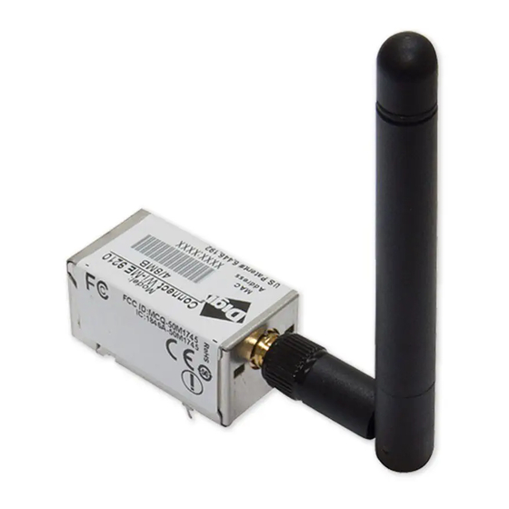
Page 12: Connectors: Antenna
Connectors: Antenna The Digi Connect Wi-ME 9210 and Digi Connect ME 9210 is available with 1 RP-SMA connector. The antenna is connected to the module with a reverse polarity SMA connector (sub-miniature size A). The antenna only fits on the module one way to ensure a proper connection. -
Page 13: Module Leds
Network Activity The LEDs are the same for a module with or without a JTAG connector. Note: LED Behaviors Digi Plug and Play Firmware Digi Connect Wi-ME 9210 and Digi Customizable Modules Connect ME 9210 Associated/Diagnostic: Same as Digi Plug-and Play On - unit is associated with an access point. -
Page 14: Chapter 3: About The Development Board
About the Development Board Overview The development board is a hardware platform from which you can determine how to integrate the embedded modules into your design. The board consists of the following main features: Socket for connecting the embedded modules ... -
Page 15: Basic Description
Basic Description The development board contains connectors, switches, and LEDs for use while integrating the embedded module into your design. See the following figure for the location of the connectors, switches, and LEDs. Additionally, the board provides test points (not shown on the figure). For more information about test points, see "Test Points"... - Page 16 Connectors, Switches and LEDs Board Description Markers 1-5 Primary Port Secondary GPIO Switch Prototyping JTAG LEDs, CR5 - Serial Port, P2 Bank, SW3 Area, P4 Header, P12 CR18 Connectors, Switches and LEDs Board Description (continued) Markers 6-10 Embedded 232 Enable JTAG Module Primary...
-
Page 17: Port Descriptions
Placement of Module Caution: When handling the development board, wear a grounding wrist strap to avoid ESD damage to the board. Port Descriptions The development board provides the following ports: Primary Serial Port, P1 Secondary Serial Port, P2 ... - Page 18 The Secondary Serial Port is a DB-9 male connector that is labeled as P2 on the development board. The port is used only with the Digi Connect ME 9210 modules with JTAG interfaces for debugging purposes. See the following figure for pin orientation; see the following table for pin assignments.
- Page 19 Secondary Serial Port Pin Assignments Pin 1 Pin 2 Pin 3 Pin 4 Pin 5 Pin 6 Pin 7 Pin 8 Pin 9 — — — — — — Signal/ — Receive Data Transmit Data — Chassis — — — —...
-
Page 20: Connectors And Blocks
The Digi Connect Wi-ME module does not provide pins 1-6 JTAG Debugger Connector, P12. -48V DC input to PoE module (Digi Connect ME 9210 must be connected to a Powering Device for this feature.), P13 12V DC output from PoE module into Dev Board Power Supply, P14 ... - Page 21 Reserved — — /INIT /INIT Digi Plug-and-Play Firmware Software Reset The Digi Connect Wi-ME module does not provide pins 1-6 Note: See "Module Pinout" on page 31 for detailed IO configuration information. Note: ...
- Page 22 Module JTAG Interface Connector, P11 The Module’s JTAG Interface Connector is a 14-pin female vertical header that is labeled P11 on the development board. The connector mates with the JTAG connector on the embedded module. The Module’s JTAG Connector pins are tied to the debugger connector (see “JTAG Debugger Connector, P12”).
- Page 23 The JTAG debugger connector is a 20-pin male vertical header that is labeled P12 on the development board. The connector mates with a JTAG debugger plug (for example, a Digi JTAG Link). The connector is used with the development kit only. See the following figure for pin orientation.
- Page 24 Logic Analyzer Header, P3 The Logic Analyzer Header is a 20-pin male vertical header that is labeled P3 on the development board. The header is for connecting a digital signal analyzer (for example, a logic analyzer) to the development board. See the following figure for pin orientation; see the following table for pin assignments.
-
Page 25: Switches And Push Buttons
Switches and Push Buttons The development board provides the following switches: User PB1 User PB2 GPIO Switch Bank 1, SW3 Reset, SW4 Power On/Off SW5 See the figure titled "Board Layout and Connector Locations:" on page 15 for the location of the switches. -
Page 26: Development Board Leds
User Push Button 2, SW2 Pushing User Push Button 2, SW2, will drive Wi-ME module pin 12 (ME module pin 18) low. Reset, SW4 The Reset switch is a push button switch labeled SW4 on the development board. Pressing the switch holds the embedded module in reset. - Page 27 Development Board LED Descriptions Board Description State Indication Label CR12 RXD, Primary Serial Port Logic 1 on TTL, mark, -V on line side CR13 DTR, Primary Serial Port Yellow Logic 1 on TTL, mark, -V on line side CR14 DTR, Primary Serial Port Green Logic 0 on TTL, space, +V on line side CR15 RTS, Primary Serial Port Yellow...
-
Page 28: Power Jack P15
Power Jack P15 The Power Jack P15 is a barrel connector that accepts 9 to 30 VDC. The following table shows the polarity of the power jack. Power Jack Polarity Contact Polarity Center +9 to +30 VDC Outer Ground The following figure schematically represents the polarity of the power jack. -
Page 29: Test Points
Test Points The development board provides 13 test points that can be identified by a board label. The test point numbers are in the development board schematic drawings. The following table lists the test point number, board label, and a brief description of each test point. Test Point Descriptions Test Board Label... -
Page 30: Chapter 4: Programming Considerations
This chapter provides information programmers may require to make use of some embedded module hardware resources. It provides programming information on the following topics for the Digi Connect ME 9210 and the Digi Connect Wi-ME 9210: "Module Pinout" on page 31 ... -
Page 31: Module Pinout
The NS7520/NS9210 processors support 16 General Purpose I/O (GPIO) lines, some of which are reserved for specific functions and some of which can be customized. For Digi Plug and Play Firmware users, see the Digi Connect Family Users Guide for details on what Pin configurations are available to you. - Page 32 GPIO [13] Timer /INIT Out 9 The CAN Bus interface is available on the 8/16 Digi Connect ME 9210, Digi Connect Note: Wi-ME 9210 variants. When using the 8/16 ME 9210/ Wi-ME 9210 CAN Bus, the DTR (9210 signal GPIO Note: 6) line must be tri-stated.
-
Page 33: Reset
Reset Hard Reset The Digi Connect Wi-ME 9210 module supports a hardware reset via pin 8 of the 14-pin header. The unit is forced into a hard reset when pulling the pin to ground, or less than 0.8v, for one microsecond. -
Page 34: Memory
Memory Flash Depending on the variant, the Digi Connect Wi-ME 9210 and Digi Connect ME 9210 have 8 or 16MB of flash memory. The Digi Connect Wi-ME 9210/ARM9 family, the flash memory is controlled by chip select 2 (default=st_cs1) and is located at 0x50000000. -
Page 35: Appendix A: Module Specifications
Antenna Connector: 1 x RP-SMA Caution: The Digi Connect Wi-ME 9210 embedded modules were designed for use in no clean flux wave soldering process. The product is not designed to support draining after a water-wash process, which can lead to water residue inside the enclosure resulting from direct entry or condensation after the wash process. -
Page 36: Serial Interface
Serial Interface One TTL serial interface (CMOS 3.3v) with full modem control signals (DTR, DSR, DCD, RTS, CTS). The Digi Connect Wi-ME 9210 also supports SPI and FIM-based application specific interfaces. Data Rates (bps) 50, 75, 110, 134, 150, 200, 300, 600, 1200, 1800, 2400, 4800, 9600, 14400,19200, 28800, 38400,... - Page 37 (3657.60 meters) Grounding Recommendation It is recommended that you connect the tabs on the chassis of the Digi Connect ME 9210/ Digi Connect Wi-ME 9210, and the ground pins directly to the logic ground plane. It is also recommended that you connect the Digi Connect ME 9210/ Digi Connect Wi-ME 9210 to the metal chassis of your enclosure.
-
Page 38: Power Management
Power Management Using the Digi NET+OS development environment, applications on the Digi Connect Wi-ME 9210 and Digi Connect ME 9210 are capable of operating the module in several reduced power consumption modes. These reduced power operating modes utilize the power management mechanisms for the NS9210 processor for CPU clock scaling and sleep. -
Page 39: Thermal Specifications
Thermal Specifications The table below shows the standard operating temperature ranges for the entire Digi Connect ME family of embedded modules. Standard Operating Temperature Ranges Product Operating Temperature Range Digi Connect Wi-ME 9210 -40C to 75C no external thermal pad... -
Page 40: Mechanical
The host PCB plays a large part in dissipating the heat generated by the module. A large copper plane located under the Digi Connect Wi-ME 9210 and soldered to the module’s mounting tabs will improve the heat dissipation capabilities of the PCB. -
Page 41: Bar Code
Dimensions The following figures show the dimensions of Digi Connect Wi-ME and Digi Connect ME 9210 module. These are the tolerances for the drawings shown on this and the following pages:... - Page 42 Side View ...
- Page 43 Bottom View ...
- Page 44 Digi Connect ME 9210Module Front View ...
- Page 45 Side View ...
- Page 46 Bottom View ...
-
Page 47: Recommended Pcb Layout
Recommended PCB Layout The following figure shows the recommended PCB (printed circuit board) layout of the Digi Connect Wi-ME. Digi Connect ME and Digi Connect Wi-ME ... -
Page 48: Antenna Information
Any antenna matching the in-band and out-of-band signal patterns and strengths of the antenna, whose characteristics are given in the Antenna Description table and the Radiation Pattern graphic may be used with the Digi Connect Wi-ME 9210. ... - Page 49 Dipole Antenna Dimensions ...
-
Page 50: Rf Exposure Statement
RF Exposure Statement The Digi Connect Wi-ME 9210 module complies with the RF exposure limits for humans as called out in RSS-102. It is exempt from RF evaluation based on its operating frequency of 2.4 GHz, and effective radiated power less than the 3 watt requirement for a mobile device (>20 cm separation) operating at 2.4 GHz. -
Page 51: Appendix B: Certifications
Consult the dealer or an experienced radio/TV technician for help. Les modules embarqués Digi Connect ME et Digi Connect Wi-ME ont été testés et approuvés dans le cadre des limites fixées par les règles de la FCC pour les dispositifs numériques de la classe B suivant la Partie 15 sous partie B. - Page 52 FCC incluse dans le module. Modifications (FCC 15.21) Changes or modifications to this equipment not expressly approved by Digi may void the user's authority to operate this equipment. Tout changement ou modification apportés à ce dispositif n'étant pas expressément approuvés par Digi peut priver l'utilisateur de mettre en œuvre cet équipement.
-
Page 53: Industry Canada
The product listed above has been tested at an External Test Laboratory certified per FCC rules and has been found to meet the FCC, Part 15, Class B, Emission Limits. Documentation is on file and available from the Digi International Homologation Department. ... - Page 54 The product listed above has been tested at an External Test Laboratory certified per FCC rules and has been found to meet the FCC, Part 15, Class B, Emission Limits. Documentation is on file and available from the Digi International Homologation Department. ...
-
Page 55: International Emc Standards
Not to exceed 95% non-condensing (4° C to 45°C), constant Relative Humidity absolute humidity above 45°C 12000 feet Altitude (3657.60 meters) The Digi Connect ME and Digi Connect Wi-ME embedded modules meet the following standards: Standards Digi Connect ME Digi Connect Wi-ME Emissions AS/NZS 3548 AS/NZS 3548 CISPR 22 FCC Part 15 Subpart C... - Page 56 The required antenna impedance is [50] ohms The following antenna configuration was tested with the Connect Wi-ME 9210 module. Digi 29000095, Bobbintron SA-006-1, +2 dBi dipole antenna (NP-SMA) To reduce potential radio interference to other users, the antenna type and its gain should be so chosen that the equivalent isotropically radiated power (e.i.r.p.) is not more than that permitted for...
-
Page 57: Appendix C: Sample Application: Poe Power Supply
Sample Application: PoE Power Supply The following schematics are examples of PoE Power Supplies: ... - Page 58 2/8 Digi Connect ME ...
- Page 59 4/8 Digi Connect ME modules and Digi Connect ME 9210 modules ...
-
Page 60: Appendix D: Sample Application: Ttl Signals To Eia-232
Sample Application: TTL Signals to EIA-232 The following schematic is an example of how to convert the modules’s TTL signals to EIA-232. ... - Page 61 ...