Renesas RL78/G1D Bluetooth Module Manuals
Manuals and User Guides for Renesas RL78/G1D Bluetooth Module. We have 9 Renesas RL78/G1D Bluetooth Module manuals available for free PDF download: User Manual, Hardware Manual
Renesas RL78/G1D User Manual (910 pages)
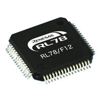
16-Bit Single-Chip Microcontrollers
Brand: Renesas
|
Category: Microcontrollers
|
Size: 6 MB
Table of Contents
Advertisement

Renesas RL78/G1D User Manual (72 pages)
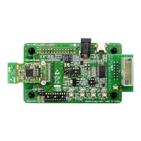
Bluetooth low energy Module
Brand: Renesas
|
Category: Control Unit
|
Size: 2 MB
Table of Contents

Renesas RL78/G1D User Manual (59 pages)
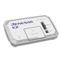
Emulator
Brand: Renesas
|
Category: Computer Hardware
|
Size: 1 MB
Table of Contents
Advertisement
Renesas RL78/G1D User Manual (58 pages)
E1/E20/E2 Emulator, E2 Emulator Lite
Brand: Renesas
|
Category: Computer Hardware
|
Size: 0 MB
Table of Contents
Renesas RL78/G1D User Manual (55 pages)
Brand: Renesas
|
Category: Computer Hardware
|
Size: 0 MB
Table of Contents

Renesas RL78/G1D User Manual (24 pages)
PowerPoint Presenter
Brand: Renesas
|
Category: Microcontrollers
|
Size: 0 MB
Table of Contents

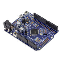
Renesas RL78/G1D User Manual (30 pages)
16-Bit Single-Chip Microcontrollers
Brand: Renesas
|
Category: Motherboard
|
Size: 2 MB
Table of Contents

Renesas RL78/G1D User Manual (31 pages)
Brand: Renesas
|
Category: Motherboard
|
Size: 2 MB
Table of Contents

Renesas RL78/G1D Hardware Manual (13 pages)
PMOD Module
Brand: Renesas
|
Category: Control Unit
|
Size: 0 MB