Renesas RL78/G16, RL78 Manual
- User manual (1879 pages) ,
- Manual (88 pages) ,
- Application note (53 pages)
Advertisement
- 1 List of Abbreviations and Acronyms
- 2 Overview
- 3 Board Layout
- 4 Parts Layout
- 5 Operating Environment
-
6
User Circuits
- 6.1 Evaluation MCU
- 6.2 USB Connector
- 6.3 Power LED
- 6.4 User LEDs
- 6.5 Capacitive Touch Buttons and Touch Slider
- 6.6 Arduino Connectors
- 6.7 Pmod Connectors
- 6.8 MCU Headers
- 6.9 Grove Connector
- 6.10 Clock
- 6.11 Reset Switch
- 6.12 User Switch
- 6.13 USB-to-Serial Converter and COM Port Debugging
- 6.14 USB-to-Serial Converter Reset Header
- 6.15 Power-Supply Selection Header
- 6.16 External Power Supply
- 6.17 Current Measurement Header
- 6.18 Pattern for Cutting the I/O Power Supply for the USB-to-Serial Converter
- 6.19 Emulator Connector
- 7 Handling Precautions
- 8 Developing Code
- 9 General Precautions in the Handling of Microprocessing Unit and Microcontroller Unit Products
- 10 Documents / Resources
List of Abbreviations and Acronyms
| Abbreviation | Full Form |
| Arduino® Uno | Connectors compatible with the Arduino® Uno R3 board are mounted on the fast prototyping board. |
| CPU | Central Processing Unit |
| DIP | Dual In-line Package |
| DNF | Do Not Fit |
| Grove | A connector that is compatible with Grove modules can be mounted on the fast prototyping board. |
| HOCO | High-Speed On-Chip Oscillator |
| IDE | Integrated Development Environment |
| IRQ | Interrupt Request |
| LOCO | Low-Speed On-Chip Oscillator |
| LED | Light Emitting Diode |
| MCU | Micro-controller Unit |
| n/a (NA) | Not applicable |
| n/c (NC) | Not connected |
| PC | Personal Computer |
| Pmod™ | Pmod™ is a trademark of Digilent Inc. The Pmod™ interface specification is the property of Digilent Inc. For the Pmod™ interface specification, refer to the Pmod™ License Agreement page at the Web site of Digilent Inc. |
| RAM | Random Access Memory |
| RFP | Renesas Flash Programmer |
| ROM | Read Only Memory |
| SPI | Serial Peripheral Interface |
| TPU | Timer Pulse Unit |
| UART | Universal Asynchronous Receiver/Transmitter |
| USB | Universal Serial Bus |
| WDT | Watchdog timer |
All trademarks and registered trademarks are the property of their respective owners.
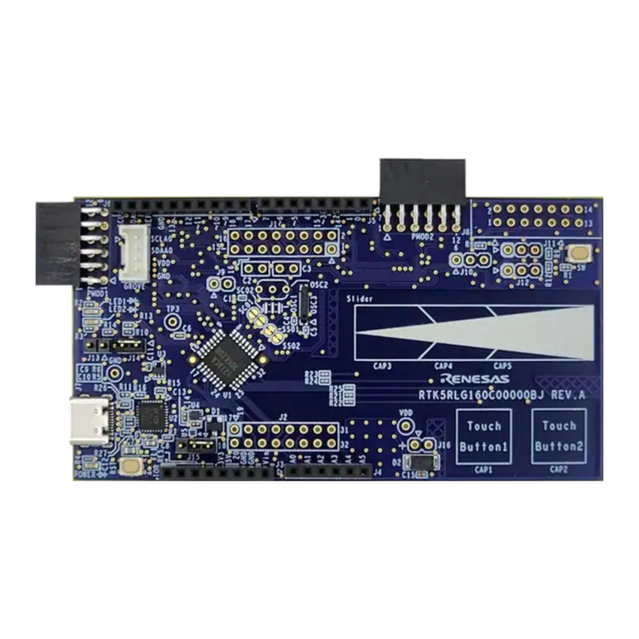
Overview
This user's manual describes the RL78/G16 Fast Prototyping Board (RTK5RLG160C00000BJ) (hereinafter referred to as "this product").
Purpose
This product is an evaluation tool for a Renesas MCU. This user's manual describes the hardware specifications, ways of setting switches, and the basic setup procedure.
Features
This product can handle the following tasks.
- Programming of the Renesas MCU
- Debugging of user code
- User circuits for switches and LEDs
- Capacitive touch button x 2
- Capacitive touch slider (with a three-electrode configuration) x 1
- Pmod™ connector*
- Arduino® connector*
- Grove connector*
Note: We do not guarantee connection to all types of these connectors. For details on the connector specifications, refer to the descriptions in this document.
Preparation
- Watch the video on "Getting Started with Fast Prototyping Board for RL78 Family".
https://www.renesas.com/video/getting-started-fast-prototyping-board-rl78-family - Install the integrated development environment (IDE) and required software on the host PC.
https://www.renesas.com/development-tools - Prepare a USB cable for data transfer.
- Refer to the following Web page and prepare the E2 emulator if required.
https://www.renesas.com/e2 - Refer to the following Web page and prepare the E2 emulator Lite if required.
https://www.renesas.com/e2lite
Installing the e2 studio IDE
For details on the procedure for installation, watch the video on "e2 studio Quick Start Guide Video for RL78 Family - Installation".
https://www.renesas.com/software-tool/rl78-software-tool-course
- Download the installer for the latest version of the e2 studio from the following Web page.
https://www.renesas.com/software-tool/e-studio - Unzip the downloaded zip file and run the installer file.
- Select "RL78" for [Device Families].
- Confirm that the latest version of Renesas CCRL has been selected as the compiler.
- Select the [I accept the terms of the Software Agreements] checkbox and then click on the [Install] button.
- When the software produces an installer window in the middle of installation, proceed with installation according to the instructions from the wizard.
- After installation has finished, click on the [OK] button.
Installing the CS+ IDE
- Download the installer for the latest version of CS+ for CC from the following Web page.
https://www.renesas.com/software-tool/cs - Unzip the downloaded zip file and run the installer file.
- Click on [Begin CS+ Startup].
- Confirm that [Tools for RL78 family] has been selected.
- After installation has finished, click on the [OK] button.
Board Specification Table
Table 1-1 shows the board specifications.
Table 1-1 Board Specification Table
| Item | Specification | |
| Evaluation MCU (RL78/G16) | Part No.: R5F121BCAFP | |
| Package: 32 pin LQFP | ||
| On chip memory: 32 KB ROM, 2 KB RAM, 1 KB data flash memory | ||
| Board size | 53.34 mm x 99.06 mm | |
| Power supply voltage | VDD: 2.4 V to 5.5 V | |
| Power supply circuit*2 | USB connector: VBUS (5 V) or 3.3 V (default) | |
| External power supply: 2.4 V to 5.5 V | ||
| E2 emulator or E2 emulator Lite | ||
| Current drawn | Max. 200 mA | |
| Main clock*1 | OSC1: Crystal oscillator (surface mount technology (SMT)) for the main system clock OSC2: Crystal oscillator or ceramic resonator (lead type) for the main system clock | |
| Sub clock | OSC3: Crystal oscillator (SMT) for the sub clock | |
| Push switches | Reset switch x 1 | |
| User switch x 1 | ||
| LEDs | Power indicator: green x 1 | |
| User: green x 2 | ||
| Capacitive touch button | 2 | A jumper block for switching the QE serial connection |
| Capacitive touch slider | 1 (with a three electrode configuration) | |
| USB connector | Connector: USB Type C | |
| Arduino® connectors | Connectors: 6 pins x 1, 8 pins x 2, 10 pins x 1 The interfaces are compatible with the Arduino® UNO R3 board. | |
| Pmod™ connectors | Connectors: Angle type, 12 pins x 2 | |
| MCU headers*1 | Headers: 16 pins (2 pins x 8 columns) x 2 | |
| USB to serial converter | Used as the interface with the RL78 COM port debug tool. FT232RQ from FTDI x 1 | |
| USB to serial converter reset header | Header: 2 pins x 1 (open circuit by default) | |
| Current measurement header*1 | Header: 2 pins x 1 | |
| Power supply selection header*2 | Header: 3 pins x 1 | |
| Emulator connector*1 | 14 pin connector for connecting an E2 emulator or E2 emulator Lite Emulator selection headers: 2 pins x 3 | |
| Grove connector | Interface for Grove modules I2C: 1 | |
Notes:
- This part is not mounted.
- The intended source of power for the evaluation MCU on the board as shipped is VBUS (5 V). Setting a jumper is required if power is to be supplied from other sources. For details, refer to Chapter "User Circuits".
Block Diagram
Figure 1-1 shows the block diagram of this product.

Board Layout
Figure 2-1 shows the external appearance of the top side of this product.

Parts Layout
Figure 3-1 shows the parts layout of this product.

Figure 3-2 shows the external dimensions of this product.

Operating Environment
Figure 4-1 shows the operating environment of this product. Install the IDE on the host PC.

User Circuits
Evaluation MCU
The specifications for the power supply, system clock, and reset of the evaluation MCU (RL78/G16) at the time of shipment are as follows.
- Power supply: 5 V (VBUS) supplied from the USB (including the analog power supply)
- System clock: Operation with an on-chip oscillator
- Reset: Directed by the reset switch or IDE
USB Connector
The connector shape is USB Type-C (support for full-speed USB 2.0). It serves as a power-supply input and an interface for communications with the RL78 COM port debug tool (through USB-to-serial conversion). Connect the USB connector to the host PC by a USB cable. If the power supply on the host side is on, the power is supplied to this product at the same time as connection of the cable.
Note: The package does not include a USB cable. Do not connect a USB cable while the emulator is supplying power.
Power LED
While the power LED is illuminated, VDD power is being supplied. The LED is green.
User LEDs
The optional user LEDs can be used for any purpose. LED1 and LED2 are mounted on the board and are respectively connected to the following ports. The LEDs are green.
- LED1: Pin 13, connected to port P12
- LED2: Pin 16, connected to port P15
Capacitive Touch Buttons and Touch Slider
The capacitive touch buttons and touch slider can be used for the user's desired purpose. Two electrodes (touch button 1 and touch button 2) and one slider (with a three-electrode configuration) are mounted on the board and are respectively connected to the following ports.
- Touch button 1: Pin 25, connected to ports P06, TS06, and CAP1
- Touch button 2: Pin 26, connected to ports P07, TS07, and CAP2
- Slider:
Pin 31, connected to ports P42, TS12, and CAP3
Pin 28, connected to ports P22, TS09, and CAP4
Pin 27, connected to ports P23, TS08, and CAP5
P02 (pin 19) is connected for the TSCAP pin function by default.
Arduino® Connectors
The specification of the Arduino® connectors is on the assumption that Arduino® shields are to be connectable. However, we do not guarantee connection to all types of Arduino® shield. Confirm the specifications of this product against any Arduino® shield you intend to use.
Figure 5-1, Table 5-1, and Table 5-2 show the pin assignments of the Arduino® connectors.

Table 5-1 Pin Assignments of the Arduino® Connectors (1/2)
| Part No. in the Circuit Schematics | Name of Arduino® Signal *1 | RL78/G16 *2 *3 | |||||
| Pin | Power Supply | Port | Analog | PWM | Serial | ||
| J3-1 | N.C. | - | - | - | - | - | - |
| J3-2 | IOREF | 8 | VDD | - | - | - | - |
| J3-3 | RESET | 3 | - | - | - | - | - |
| J3-4 | 3V3 | - | - | - | - | - | - |
| J3-5 | 5V | - | - | - | - | - | - |
| J3-6 | GND | 7 | VSS | - | - | - | - |
| J3-7 | GND | 7 | VSS | - | - | - | - |
| J3-8 | VIN | - | - | - | - | - | - |
| J4-1 | A0 | 24 | - | P05 | ANI4 | - | - |
| J4-2 | A1 | 19 | - | (P02) *4 | (ANI1) *4 | - | - |
| J4-3 | A2 | 25 | - | (P06) | (ANI5) | - | - |
| J4-4 | A3 | 26 | - | (P07) | (ANI6) | - | - |
| J4-5 | A4 | 27 | - | (P23) | (ANI7) | - | - |
| J4-6 | A5 | 28 | - | (P22) | (ANI8) | - | - |
Notes:
- "x" in IOx and IO~x means a pin number for the Arduino IDE. For more information about Arduino IDE please refer to the following URL: https://github.com/renesas/Arduino/wiki/
- Short-circuit the short-circuit pads for signals with names enclosed in parentheses, "()".
- When using a signal with "[]", require PIORx register setting.
- P02 is connected to a 0.01-uF capacitor by default. When P02 is to be used as a port pin, short-circuit the short-circuit pad [SC06]. Note that P02 cannot be used as PCLBUZ0 because it is connected to the 0.01-uF capacitor.
Table 5-2 Pin Assignments of the Arduino® Connectors (2/2)
| Part No. in the Circuit Schematics | Name of Arduino® Signal *1 | RL78/G16 *2 *3 | |||||
| Pin | Power Supply | Port | Analog | PWM | Serial | ||
| J5-1 | RX/0 | 23 | - | P04 | - | - | [RxD0] |
| J5-2 | TX/1 | 22 | - | P03 | - | - | [TxD0] |
| J5-3 | 2 | 12 | - | P11/INTP9 | - | - | - |
| J5-4 | ~3 | 11 | - | P10/INTP8 | - | [TO03] | - |
| J5-5 | 4 | 15 | - | P14 | - | - | - |
| J5-6 | ~5 | 20 | - | P16 | - | [TO03] | - |
| J5-7 | ~6 | 21 | - | P17 | - | [TO04] | - |
| J5-8 | 7 | 31 | - | (P42) | - | - | - |
| J6-1 | 8 | 1 | - | P43 | - | - | - |
| J6-2 | ~9 | (5) | - | (P122) *4 | - | (TO05) *4 | - |
| J6-3 | ~10 | (6) | - | (P121) *4 | - | (TO07) *4 | - |
| J6-4 | ~11 | 29 | - | P21 | - | [TO00] | SO20 |
| J6-5 | 12 | 30 | - | P20 | - | - | SI20 |
| J6-6 | 13 | 32 | - | P41 | - | - | SCK20 |
| J6-7 | GND | - | VSS | GND | - | - | - |
| J6-8 | ADREF | - | - | - | - | - | - |
| J6-9 | SDA | 10 | - | P61 | - | - | SDAA0 |
| J6-10 | SCL | 9 | - | P60 | - | - | SCLA0 |
Notes:
- "x" in IOx and IO~x means a pin number for the Arduino IDE. For more information about Arduino IDE please refer to the following URL: https://github.com/renesas/Arduino/wiki/
- Short-circuit the short-circuit pads for signals with names enclosed in parentheses, "()".
- When using a signal with "[]", require PIORx register setting.
- P121, P122 is connected to the XT1, XT2 sub-clock by default. When P121, P122 is to be used as a port pin, cut the pattern for cutting [SS01], [SS02] and short-circuit the short-circuit pad [SS09], [SC10].
Pmod™ Connectors
The specification of the Pmod™ connectors is on the assumption that Pmod™ modules are to be connectable.
Pmod1 is assumed to be connected to the Pmod™ Interface Type 2A or 3A module*.
Pmod2 is assumed to be connected to the Pmod™ Interface Type 6A module*.
Note: For details on the Pmod™ module from Renesas, refer to the Web site at: https://www.renesas.com/quickconnect.
However, we do not guarantee connection to all types of Pmod™ module. Confirm the specifications of this product against any Pmod™ module you intend to use.
Figure 5-2, Table 5-3, and Table 5-4 show the pin assignments of the Pmod™ connectors.

Note: Using the signal names enclosed in parentheses, "()", requires switching the wiring by using the shortcircuit pads.
Table 5-3 Pin Assignments of Pmod™ (Pmod1)
| Pin No. of Pmod™ | Name of Pmod™ Signal | RL78/G16 *2 | |||||
| Pin | Power Supply | Port | SPI (CSI) | UART | I2C | ||
| 1 | CS/CTS | 14 | - | P13 | - | - | [INTP4] |
| 2 | MOSI/TXD | 22 | - | P03 | [SO00] | [TxD0] | - |
| 3 | MISO/RXD | 23(25) *1 | - | P04(P06) *1 | [SI00] | [RxD0] | ([SCLA0]) *1 |
| 4 | SCK/RTS | 24(26) *1 | - | P05(P07) *1 | [SCK00] | - | ([SDAA0]) *1 |
| 5 | GND | - | VSS | - | - | - | - |
| 6 | VCC | - | VDD | - | - | - | - |
| 7 | INT/GPIO | 15 | - | P14 | [INTP2] | [INTP2] | - |
| 8 | RESET | 21 | - | P17 | - | - | - |
| 9 | GPIO | 20 | - | P16 | - | - | - |
| 10 | GPIO | 16 | - | P15 | - | - | - |
| 11 | GND | - | EVSS | - | - | - | - |
| 12 | VCC | - | VDD | - | - | - | - |
Note:
- These signals can be used as Type 6A (I2C) by cutting the patterns for cutting [SS05] and [SS06] and shortcircuiting the short-circuit pads [SC04] and [SC05].
- When using a signal with "[]", require PIORx register setting.
Table 5-4 Pin Assignments of Pmod™ (Pmod2)
| Pin No. of Pmod™ | Name of Pmod™ Signal | RL78/G16 | |||||
| Pin | Power Supply | Port | SPI (CSI) | UART | I2C | ||
| 1 | INT | 11 | - | P10 | - | - | INTP8 |
| 2 | RESET | 29 | - | P21 | SO20 | TxD2 | - |
| 3 | SCL | 9(30) *1 | - | P60(P20) *1 | (SI20) *1 | (RxD2) *1 | SCLA0 |
| 4 | SDA | 10(32) *1 | - | P61(P41) *1 | (SCK20) *1 | - | SDAA0 |
| 5 | GND | - | VSS | - | - | - | - |
| 6 | VCC | - | VDD | - | - | - | - |
| 7 | IO1 | 12 | - | P11 | INTP9 | INTP9 | - |
| 8 | IO2 | 1 | - | P43 | - | - | - |
| 9 | IO3 | 4 | - | P137 | - | - | - |
| 10 | IO4 | 13 | - | P12 | - | - | - |
| 11 | GND | - | VSS | - | - | - | - |
| 12 | VCC | - | VDD | - | - | - | - |
Note:
- These signals can be used as Type 2A or 3A (SPI or UART) by cutting the patterns for cutting [SS24] and [SS25] and short-circuiting the short-circuit pads [SC17] and [SC18].
MCU Headers
The MCU headers are provided as through holes J1 and J2 for a total of 16 (8 x 2) pins. The pin headers have a pitch of 2.54 mm and the evaluation MCU is connected to the through holes for the headers.
Table 5-5 and Table 5-6 show the pin assignments of the MCU headers.
Table 5-5 Pin Assignments of the MCU Header (J1)
| Part No. in the Circuit Schematics | Name of Arduino® Signal*1 | RL78/G16 | |||
| Pin | Power Supply | Port and Peripheral Modules | Others | ||
| J1-1 | 8 | 1 | - | P43/TS14 | - |
| J1-2 | 14 | 2 | - | P40/TOOL0/INTP2/(TI01/TO01)/(PCLBUZ0) | TOOL0 |
| J1-3 | - | 3 | - | P125*4/RESET/(INTP0)/INTP1/(VCOUT0)/(VCOUT1)/(SI11) | RST |
| J1-4 | 15 | 4 | - | P137/INTP0/TI00 | SW |
| J1-5 | ~9 | 5 | - | P122/X2/XT2/EXCLK/EXCLKS/(INTP2)/TI05/TO05*2 | XT2 |
| J1-6 | ~10 | 6 | - | P121/X1/XT1/(INTP3)/(INTP4)/(INTP5)/TI07/TO07*3 | XT1 |
| J1-7 | - | 7 | VSS | VSS | - |
| J1-8 | - | 8 | VDD | VDD | - |
| J1-9 | SCL | 9 | - | P60/(INTP3)/(INTP6)/(SI11)/SCLA0 | - |
| J1-10 | SDA | 10 | - | P61/(INTP7)/(SO11)/(SDA11)/SDAA0 | - |
| J1-11 | ~3 | 11 | - | P10/INTP8/(TI03/TO03)/(SCK11/SCL11)/(RXD1)/(PCLBUZ0) | - |
| J1-12 | 2 | 12 | - | P11/INTP9/(TI03/TO03)/(SCK11/SCL11)/(TXD1)/(PCLBUZ0)/( RTC1HZ) | - |
| J1-13 | 16 | 13 | - | P12/(INTP8) | LED1 |
| J1-14 | 17 | 14 | - | P13/(INTP2)/(INTP4)/(SCL11/SCK11)/(SCK20/SCL20)/(RTC1 HZ) | - |
| J1-15 | 4 | 15 | - | P14/(INTP2)/(SI11/SDA11)/(SI20/RXD2/SDA20) | - |
| J1-16 | 18 | 16 | - | P15/(INTP9)/(SO11)/(SO20/TXD2) | LED2 |
Notes:
- The names of the Arduino® signals correspond to the pin numbers for the Arduino® IDE. For more information about Arduino® IDE please refer to the following URL: https://github.com/renesas/Arduino/wiki/
- P122 is connected to the XT2 sub-clock by default. When P122 is to be used as a port pin, cut the pattern for cutting [SS02] and short-circuit the short-circuit pad [SC10].
- P121 is connected to the XT1 sub-clock by default. When P121 is to be used as a port pin, cut the pattern for cutting [SS01] and short-circuit the short-circuit pad [SC09].
- When the RL78 COM port debug tool is in use, use of the P125/RESET pin as P125 is prohibited. If P125 is mistakenly set, please refer to USB-to-Serial Converter and COM Port Debugging.
Table 5-6 Pin Assignments of the MCU Headers (J2)
| Part No. in the Circuit Schematics | Name of Arduino® Signal*1 | RL78/G16 | |||
| Pin | Power Supply | Port and Peripheral Modules | Others | ||
| J2-17 | 19 | 17 | - | P00/INTP6/(TI02/TO02)/SO00/TXD0/TOOLTXD/(SCK11/SCL 11)/(SI11/SDA11)/(SCLA0)/(RTC1HZ) | TOOLTxD |
| J2-18 | 20 | 18 | - | P01/ANI0/INTP5/(TI01/TO01)/TI02/TO02/SI00/RXD0/TOOLR XD/SDA00/(SI11/SDA11)/(SO11)/(SDAA0)/TS00 | TOOLRxD |
| J2-19 | A1 | 19 | - | P02/ANI1/INTP7/TI01/TO01/(TI02/TO02)/SCK00/SCL00/(SO1 1)/(SCK20/SCL20)/PCLBUZ0/VCOUT0/TSCAP*2 | TSCAP |
| J2-20 | ~5 | 20 | - | P16/(TI03/TO03)/(SI20/RxD2/SDA20)/(SCLA0)/TS01 | - |
| J2-21 | ~6 | 21 | - | P17/(TI04/TO04)/(SO20/TxD2)/(SDAA0)/TS02 | - |
| J2-22 | TX_1 | 22 | - | P03/ANI2/IVCMP0/INTP4/(TI00)/TO00/(TI05/TO05)/(SO00/TX D0)/RxD1/TS03 | - |
| J2-23 | RX_0 | 23 | - | P04/ANI3/IVREF0/INTP3/(TI01/TO01)/TI06/TO06/(SI00/RXD0 /SDA00)/(SO00/TXD0)/TxD1/TS04 | - |
| J2-24 | A0 | 24 | - | P05/ANI4/IVCMP1/(INTP6)/(TI02/TO02)/(TI07/TO07)/(SCK00/ SCL00)/(SI00/RXD0/SDA00)/SO11/TS05 | - |
| J2-25 | A2 | 25 | - | P06/ANI5/IVREF1/(INTP7)/(TI03/TO03)/(SCK00/SCL00)/SI11/ SDA11/(SCLA0)/(PCLBUZ0)/TS06*3 | CAP1 (Touch Button 1) |
| J2-26 | A3 | 26 | - | P07/ANI6/(INTP5)/(TO03)/TI04/TO04/SCK11/SCL11/(SDAA0) /VCOUT1/TS07*3 | CAP2 (Touch Button 2) |
| J2-27 | A4 | 27 | - | P23/ANI7/(INTP6)/(TI04/TO04)/(SCL11)/TS08*3 | CAP5 (Touch Slider 3) |
| J2-28 | A5 | 28 | - | P22/ANI8/(INTP5)/(TI06/TO06)/(SDA11)/TS09*3 | CAP4 (Touch Slider 2) |
| J2-29 | MOSI_~11 | 29 | - | P21/ANI9/(INTP7)/(TO00)/(RxD1)/SO20/TXD2/TS10 | - |
| J2-30 | MSO_12 | 30 | - | P20/ANI10/(INTP1)/(TI00)/(TO00)/(TI03/TO03)/(SCK11/SCL1 1)(RxD1)/(TxD1)/SI20/RXD2/SDA20/TS11 | - |
| J2-31 | 7 | 31 | - | P42/(TI00)/(TxD1)/TS12*3 | CAP3 (Touch Slider 1) |
| J2-32 | 13 | 32 | - | P41/(INTP3)/(INTP4)/(TI02/TO02)/TI03/TO03/(SO11)/(SDA11 )/SCK20/SCL20/RTC1HZ/(VCOUT0)/(VCOUT1)/TS13 | - |
Notes:
- The names of the Arduino® signals correspond to the pin numbers for the Arduino® IDE. For more information about Arduino® IDE please refer to the following URL: https://github.com/renesas/Arduino/wiki/
- P02 is connected to a 0.01-uF capacitor by default. When P02 is to be used as a port pin, short-circuit the short-circuit pad [SC06]. Note that P02 cannot be used as PCLBUZ0 because it is connected to the 0.01-uF capacitor.
- When these signals are to be used as port pins, short-circuit the short-circuit pads [SC12], [SC11], [SC15], [SC13], and [SC14].
Grove Connector
The specification of the grove connector is on the assumption that Grove modules are to be connectable through I2C. If a connector is mounted, however, connection to all Grove modules (through I2C) is not guaranteed. Use this connector after having confirmed the specifications of this product and Grove modules (through I2C) you intend to use.
Figure 5-3 and Table 5-7 show the pin assignments of the Grove connector.

Table 5-7 Pin Assignments of the Grove Connector
| Part No. in the Circuit Schematics | RL78/G16 | |||
| Pin | Power Supply | Port | I2C | |
| GROVE-1 | 9 | - | P60 | SCLA0 |
| GROVE-2 | 10 | - | P61 | SDAA0 |
| GROVE-3 | - | VDD | - | - |
| GROVE-4 | - | GND | - | - |
Clock
Clock circuits are provided to handle the clock sources for the evaluation MCU. For details on the specifications of the evaluation MCU clocks, refer to the RL78/G16 User's Manual: Hardware. For details on the clock circuit of this product, refer to the circuit schematics of the RL78/G16 Fast Prototyping Board. Table 5-8 shows the details of the clocks on the RL78/G16 Fast Prototyping Board.
Table 5-8 Details of Clocks
| Clock | Function and Usage | State as Shipped | Frequency | Package for the Oscillator |
| OSC1* | Crystal oscillator for the main system clock (e.g. CSTNE12M0G52x from Murata Manufacturing Co., Ltd.) | Not mounted | n/a | SMT |
| OSC2* | Crystal oscillator or ceramic resonator for the main system clock (e.g. CSTLS10M0G53x from Murata Manufacturing Co., Ltd.) | Not mounted | n/a | Lead type |
| OSC3 | Crystal oscillator for the sub clock | Mounted | 32.768 kHz | SMT |
Note: Use the main system clock by cutting the patterns for cutting [SS01] and [SS02] and short-circuiting the shortcircuit pads [SC01] and [SC02]. Note that the main system clock cannot be used at the same time as the subclock.
Reset Switch
Pressing the reset switch (RST) applies a hardware reset to the evaluation MCU.
User Switch
An optional user switch (SW) is mounted. It is connected to pin 4 of the evaluation MCU, which operates as pin function P137. The INTP0 interrupt is multiplexed on the same pin.
USB-to-Serial Converter and COM Port Debugging
A USB-to-serial converter (FT232RQ) from FTDI is mounted on the board and is usable with the standard driver of Windows 10. For other operating systems, install the driver by downloading from the following Web site of FTDI.
https://www.ftdichip.com/
DRIVERS > VCP Drivers
The USB-to-serial converter reset header (J13) is open-circuit; it is recognized as a COM port when the host PC is connected to this board via a USB cable.
As the interface with the RL78 COM port debug tool, the USB-to-serial converter enables debugging and programming of the evaluation MCU. Refer to Chapter "Developing Code". Note that the P40, P01, and P00 pins of the evaluation MCU are respectively occupied as the TOOL0, TOOLRxD, and TOOLTxD functions.
When the RL78 COM port debug tool is in use, use of the P125/RESET pin as the P125 port pin is prohibited. Do not make the option byte setting for using P125.
If P125 is mistakenly set, COM port debugging and writing will become unavailable. If you are unable to use COM port debugging or writing, please recover by erasing the program using an E2 emulator or E2 emulator Lite connection, or by using the 'COM Port Connection Recovery Application for Fast Prototyping Board' (R01AN7363).
For the method of COM port debugging, refer to the application note, RL78 Debugging Functions Using the Serial Port (R20AN0632).
When the USB-to-serial converter is not used as the interface with the RL78 COM port debug tool, using the RxD0 and TxD0 functions of the P01 and P00 pins enables UART communications between the host PC and the evaluation MCU. The user needs to prepare the terminal software, such as TeraTerm.
USB-to-Serial Converter Reset Header
The USB-to-serial converter is placed in the forced reset state by short-circuiting its reset header (J13). If the evaluation MCU alone is to operate without the use of the RL78 COM port debug tool, place the USB-to-serial converter in the reset state. This allows the use of P01 (RxD0) and P00 (TxD0) as facilities other than for a UART, such as port pins, while a reset is being applied to the USB-to-serial converter. Even if P11 and P12 are used as facilities other than for a UART, such as port pins, the board must be connected to the host PC by using the USB cable. Figure 5-4 shows the position of the USB-to-serial converter reset header.

Power-Supply Selection Header
The operating power (VDD) of the evaluation MCU can be changed to supply from the emulator or external power, and to 5 V or 3.3 V with the use of a header (J15). Only change the jumper setting of J15 while power is not being supplied.
- 1-2 of J15 being short-circuit selects a 5-V power supply. This is the default setting as shipped.

- 2-3 of J15 being short-circuit selects a 3.3-V power supply.
![]()
- J15 being open-circuit selects supply from the emulator or external power.
![]()


External Power Supply
When the evaluation MCU is to have a desired power-supply voltage, or when more current is required, use an external power supply. The usable voltages depend on the evaluation MCU.
Destinations for the connection of an external power supply:
- VDD: pin J16-1 on the external power-supply header
- VSS: pin J16-2 on the external power-supply header
Figure 5-8 shows the positions of the external power supply.
When an external power supply is used, confirm that the I/O voltages for Arduino® shields, Pmod™ modules, or Grove modules are correct.

Current Measurement Header
This header (J9) is used to measure the current drawn by the evaluation MCU (J9 header components are not mounted). Connecting an ammeter to this product enables measurement of the current being drawn by the evaluation MCU. Take care to cut the given pattern for cutting (SS18) if this header is to be used. Figure 5-9 shows the positions of the current measurement header and pattern for cutting.

Insert an ammeter between the sockets of the current measurement header (J9) to measure the current. Cut the pattern for cutting (SS18) (Figure 5-11) and turn down the LED to reduce the current drawn with an MCU other than the evaluation MCU.
Figure 5-10 is a block diagram of the power-supply lines related to the measurement of current drawn. For a block diagram of the power-supply circuit as a whole, refer to Figure 6-2.

Pattern for Cutting the I/O Power Supply for the USB-to-Serial Converter
If you intend to use this board without connecting a USB connector, cut the given pattern for cutting (SS14). Figure 5-11 shows the position of the pattern for cutting.

Emulator Connector
This 14-pin connector (J8) is used to connect this product to an on-chip debugging E2 emulator or E2 emulator Lite, from Renesas Electronics, incorporating programming facilities. The emulator is used for programming or debugging the evaluation MCU.
To connect the emulator, change the circuit as follows.
- J8: 14-pin connector must be mounted
- J10, J11, and J12: pins 2-3 are short-circuit
- Pattern for cutting [SS28]: cut
- Pattern for cutting [SS29]: cut
- Pattern for cutting [SS30]: cut

For the usage of the emulator, refer to the E1/E20/E2 Emulator, E2 emulator Lite Additional Document for User's Manual (Notes on Connection of RL78) (R20UT1994).
If you use COM port debugging with the use of the USB-to-serial converter, make the following change to settings as follows.
- J10, J11, and J12: pins 1-2 are short-circuit


Handling Precautions
Power to be Supplied
When power is supplied to this product from an emulator or through the USB, note that the total current of VDD, 5 V, and 3.3 V should not exceed the maximum current of 200 mA.
Remodeling the Board
Any modification of the board (including cutting the patterns for cutting) shall be conducted at the user's own responsibility.
The following shows the settings of jumpers as shipped.
- J13: open-circuit
- J14: short-circuit
- J15: pins 1-2 are short-circuit
In this document, "short-circuit pads" refers to pairs of pads for short-circuiting by solder.
"Pattern for cutting" refers to a narrow signal pattern in the middle part between two short-circuit pads. When you cut the pattern for cutting, do not cut over the silkscreened frame of a white ellipse.

In some cases, a pattern for cutting may not be visible because it has been covered with coating of a resist. Also refer to the circuit schematics.
In the circuit schematics, the symbol below indicates that there is a pattern for cutting between short-circuit pads.

In the circuit schematics, the symbol below indicates that there are only short-circuit pads without any pattern for cutting.

Power Supplies and Usage Conditions
Different power supplies can be selected. Table 6-1 shows the relationship between power-supply sources and usage conditions.
Figure 6-2 shows the block diagram of the power-supply circuit.

Table 6-1 Power-Supply Sources and Usage Conditions
| Power-Supply Source | Usage Condition | ||||
| Power supplied to the evaluation MCU | Use of Arduino® shields*1 | Use of Pmod™ or Grove modules*1 | Use of an emulator and IDE | Jumper setting*2 | |
| USB*4 (default) | 5 V or 3.3 V | Possible | Possible | Possible*3 | Not required
|
| External power supply | 2.4 V to 5.5 V | Possible | Possible | Possible*3 | Required
|
| Emulator | E2 Lite: 3.3 V E2: 2.4 V to 5.0 V | Not possible | Possible | Possible | Required
|
Notes:
- Connecting the RL78/G16 Fast Prototyping Board to an Arduino® shield, a Pmod™ module, or a Grove module shall be conducted at the user's own responsibility and should only proceed after confirming the specifications of the power supply and interfaces. When an Arduino® shield requires the supply of 5-V or 3.3-V power, connect the host PC to this board via the USB cable.
- Requirements for modifications after shipment are stated in this column.
- Use the IDE in a state where power is being supplied from a source other than the emulator.
- If power to be supplied to this product other than via the USB, cut the pattern for cutting (SS14).
Note on Using QE for Capacitive Touch
When you are using QE for Capacitive Touch (QE) with this product, change the circuits in the following cases (1) and (2).
For the methods for developing touch applications with the use of QE in the RL78/G16 MCU, refer to the application note "RL78 Family Using the standalone version of QE to Develop Capacitive Touch Applications" (R01AN6574).
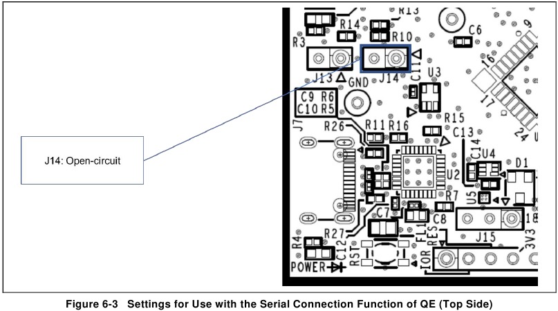
- Usage with the serial connection function of QE
When the serial connection function of QE is to be used (serial communications via QE between the host PC and the USB connector on the board of this product), modify the J14 jumper block for switching the QE serial connection as follows.- J14: open-circuit
![]()
Note: When the circuit is configured for the case "(1) Usage with the serial connection function of QE" above, the following form of usage is not available with QE.- Debugging or programming through COM port debugging
- J14: open-circuit
- Not using the serial connection function of QE
After the changes to the circuit have been made as described under "(1) Usage with the serial connection function of QE", if you want to restore the settings to those for COM port debugging (including the case of the usage described under note above), make the following change of setting as follows.- J14: short-circuit

- J14: short-circuit

Note on Using P00/TxD0
When the power is turned on or immediately after release from resetting of the USB-to-serial converter of this product, if a user program which starts the output of the UART transmission to the P00/TxD0 line is written to the target MCU before the host PC recognizes the USB-to-serial converter as the COM port, the operation of the USB-to-serial converter may be unstable and prevent connection to the Renesas Flash Programmer or terminal software.
In such cases, turn on the power (connect the USB cable) while pressing the reset switch, wait about 3 seconds until the host PC recognizes the USB-to-serial converter as the COM port, and release the reset switch. Otherwise, reset the USB-to-serial converter (by briefly short-circuiting J13 and then restored it to open-circuit) while pressing the reset switch, wait about 3 seconds until the host PC recognizes the USB-toserial converter as the COM port, and release the reset switch.
Finally, erase the user program by using the Renesas Flash Programmer.
Developing Code
Use the e2 studio or CS+, both of which support the evaluation MCU (RL78/G16).
For the usage of the E2 emulator and E2 emulator Lite, refer to the help system or user's manual of the e2 studio or CS+.
Using COM Port Debugging with the e2 studio
Figure 7-1 shows the settings of the e2 studio when it is to be connected to the RL78/G16 Fast Prototyping Board.

- [Debug hardware]: Select [COM port (RL78)].
- [Target Device]: Select [R5F121BC].
- [Connection with Target Board]: [COM Port]: Select the COM port number for assignment to the RL78/G16 FPB from the pull-down list. [Reset control pin]: Select [DTR].
Using COM Port Debugging with CS+
Figure 7-2 and Figure 7-3 show the settings of CS+ when it is to be connected to the RL78/G16 Fast Prototyping Board.
- [Using Debug Tool]:
Select [RL78 COM Port] from [Using Debug Tool] in the [Debug] menu.
![]()
- [Connection with Target Board]:
[Communication port]: Select the COM port number for assignment to the RL78/G16 FPB from the pulldown list.
[Reset control pin]: Select [DTR].
![]()


For details and points for caution, refer to the following application note for the RL78 COM port debug tool.
- RL78 Debugging Functions Using the Serial Port (R20AN0632)
General Precautions in the Handling of Microprocessing Unit and Microcontroller Unit Products
The following usage notes are applicable to all Microprocessing unit and Microcontroller unit products from Renesas. For detailed usage notes on the products covered by this document, refer to the relevant sections of the document as well as any technical updates that have been issued for the products.
- Precaution against Electrostatic Discharge (ESD)
A strong electrical field, when exposed to a CMOS device, can cause destruction of the gate oxide and ultimately degrade the device operation. Steps must be taken to stop the generation of static electricity as much as possible, and quickly dissipate it when it occurs. Environmental control must be adequate. When it is dry, a humidifier should be used. This is recommended to avoid using insulators that can easily build up static electricity. Semiconductor devices must be stored and transported in an anti-static container, static shielding bag or conductive material. All test and measurement tools including work benches and floors must be grounded. The operator must also be grounded using a wrist strap. Semiconductor devices must not be touched with bare hands. Similar precautions must be taken for printed circuit boards with mounted semiconductor devices. - Processing at power-on
The state of the product is undefined at the time when power is supplied. The states of internal circuits in the LSI are indeterminate and the states of register settings and pins are undefined at the time when power is supplied. In a finished product where the reset signal is applied to the external reset pin, the states of pins are not guaranteed from the time when power is supplied until the reset process is completed. In a similar way, the states of pins in a product that is reset by an on-chip power-on reset function are not guaranteed from the time when power is supplied until the power reaches the level at which resetting is specified. - Input of signal during power-off state
Do not input signals or an I/O pull-up power supply while the device is powered off. The current injection that results from input of such a signal or I/O pull-up power supply may cause malfunction and the abnormal current that passes in the device at this time may cause degradation of internal elements. Follow the guideline for input signal during power-off state as described in your product documentation. - Handling of unused pins
Handle unused pins in accordance with the directions given under handling of unused pins in the manual. The input pins of CMOS products are generally in the high-impedance state. In operation with an unused pin in the open-circuit state, extra electromagnetic noise is induced in the vicinity of the LSI, an associated shoot-through current flows internally, and malfunctions occur due to the false recognition of the pin state as an input signal become possible. - Clock signals
After applying a reset, only release the reset line after the operating clock signal becomes stable. When switching the clock signal during program execution, wait until the target clock signal is stabilized. When the clock signal is generated with an external resonator or from an external oscillator during a reset, ensure that the reset line is only released after full stabilization of the clock signal. Additionally, when switching to a clock signal produced with an external resonator or by an external oscillator while program execution is in progress, wait until the target clock signal is stable. - Voltage application waveform at input pin
Waveform distortion due to input noise or a reflected wave may cause malfunction. If the input of the CMOS device stays in the area between VIL (Max.) and VIH (Min.) due to noise, for example, the device may malfunction. Take care to prevent chattering noise from entering the device when the input level is fixed, and also in the transition period when the input level passes through the area between VIL (Max.) and VIH (Min.). - Prohibition of access to reserved addresses
Access to reserved addresses is prohibited. The reserved addresses are provided for possible future expansion of functions. Do not access these addresses as the correct operation of the LSI is not guaranteed. - Differences between products
Before changing from one product to another, for example to a product with a different part number, confirm that the change will not lead to problems. The characteristics of a microprocessing unit or microcontroller unit products in the same group but having a different part number might differ in terms of internal memory capacity, layout pattern, and other factors, which can affect the ranges of electrical characteristics, such as characteristic values, operating margins, immunity to noise, and amount of radiated noise. When changing to a product with a different part number, implement a systemevaluation test for the given product.
Renesas RL78/G16 Fast Prototyping Board Disclaimer
By using this RL78/G16 Fast Prototyping Board, the User accepts the following terms, which are in addition to, and control in the event of disagreement, with Renesas' General Terms and Conditions available at renesas.com/legal-notices.
The RL78/G16 Fast Prototyping Board is not guaranteed to be error free, and the entire risk as to the results and performance of the RL78/G16 Fast Prototyping Board is assumed by the User. The EK RA2L2 is provided by Renesas on an "as is" basis without warranty of any kind whether express or implied, including but not limited to the implied warranties of good workmanship, fitness for a particular purpose, title, merchantability, and non-infringement of intellectual property rights. Renesas expressly disclaims any implied warranty.
Renesas does not consider the RL78/G16 Fast Prototyping Board to be a finished product and therefore the RL78/G16 Fast Prototyping Board may not comply with some requirements applicable to finished products, including, but not limited to recycling, restricted substances and electromagnetic compatibility regulations. Refer to Certifications section, for information about certifications and compliance information for the RL78/G16 Fast Prototyping Board. It is the kit User's responsibility to make sure the kit meets any local requirements applicable to their region.
Renesas or its affiliates shall in no event be liable for any loss of profit, loss of data, loss of contract, loss of business, damage to reputation or goodwill, any economic loss, any reprogramming or recall costs (whether the foregoing losses are direct or indirect) nor shall Renesas or its affiliates be liable for any other direct or indirect special, incidental or consequential damages arising out of or in relation to the use of this RL78/G16 Fast Prototyping Board, even if Renesas or its affiliates have been advised of the possibility of such damages.
Renesas has used reasonable care in preparing the information included in this document, but Renesas does not warrant that such information is error free nor does Renesas guarantee an exact match for every application or parameter to part numbers designated by other vendors listed herein. The information provided in this document is intended solely to enable the use of Renesas products. No express or implied license to any intellectual property right is granted by this document or in connection with the sale of Renesas products. Renesas reserves the right to make changes to specifications and product descriptions at any time without notice. Renesas assumes no liability for any damages incurred by you resulting from errors in or omissions from the information included herein. Renesas cannot verify, and assumes no liability for, the accuracy of information available on another company's website.
Precautions
This Evaluation Kit is only intended for use in a laboratory environment under ambient temperature and humidity conditions. A safe separation distance should be used between this and any sensitive equipment. Its use outside the laboratory, classroom, study area, or similar such area invalidates conformity with the protection requirements of the Electromagnetic Compatibility Directive and could lead to prosecution.
The product generates, uses, and can radiate radio frequency energy and may cause harmful interference to radio communications. There is no guarantee that interference will not occur in a particular installation. If this equipment causes harmful interference to radio or television reception, which can be determined by turning the equipment off or on, you are encouraged to try to correct the interference by one or more of the following measures:
- Ensure attached cables do not lie across the equipment.
- Reorient the receiving antenna.
- Increase the distance between the equipment and the receiver.
- Connect the equipment into an outlet on a circuit different from that which the receiver is connected.
- Power down the equipment when not in use.
- Consult the dealer or an experienced radio/TV technician for help.
Note: It is recommended that wherever possible shielded interface cables are used.
The product is potentially susceptible to certain EMC phenomena. To mitigate against them it is recommended that the following measures be undertaken:
- The user is advised that mobile phones should not be used within 10 m of the product when in use.
- The user is advised to take ESD precautions when handling the equipment.
The Evaluation Kit does not represent an ideal reference design for an end product and does not fulfill the regulatory standards for an end product.
Corporate Headquarters
TOYOSU FORESIA, 3-2-24 Toyosu,
Koto-ku, Tokyo 135-0061, Japan
www.renesas.com
Contact information
For further information on a product, technology, the most up-to-date version of a document, or your nearest sales office, please visit:
www.renesas.com/contact/.
Documents / Resources
References
Getting Started with Fast Prototyping Board for RL78 Family | Renesas
Development Tools | Renesas
E2 emulator [RTE0T00020KCE00000R] | Renesas
E2 emulator Lite [RTE0T0002LKCE00000R] | Renesas
RL78 Family Software & Tool Course | Renesas
e² studio | Renesas
CS+ | Renesas
![github.com]() Home · renesas/Arduino Wiki · GitHub
Home · renesas/Arduino Wiki · GitHubQuickConnect Platform | Renesas
![www.ftdichip.com]() Home - FTDI
Home - FTDILegal Notices | Renesas
Renesas Electronics Corporation | Renesas
Contact Us | Renesas
Download manual
Here you can download full pdf version of manual, it may contain additional safety instructions, warranty information, FCC rules, etc.
Advertisement


Need help?
Do you have a question about the RL78 Series and is the answer not in the manual?
Questions and answers