iWave iW-RainboW-G35D Hardware User's Manual
Zynq ultrascale+ mpsoc (zu11/17/19eg) som development platform
Hide thumbs
Also See for iW-RainboW-G35D:
- Hardware user's manual (102 pages) ,
- Hardware user's manual (110 pages)

Related Manuals for iWave iW-RainboW-G35D


Summary of Contents for iWave iW-RainboW-G35D
- Page 1 Zynq Ultrascale+ MPSoC (ZU11/17/19EG) SOM DevKit Hardware User Guide iW-RainboW-G35D Zynq Ultrascale+ MPSoC (ZU11/17/19EG) SOM Development Platform Hardware User Guide REL0.2 iWave Systems Technologies Pvt. Ltd. Page 1 of 110...
- Page 2 If you are not the intended recipient (or authorized to receive for the recipient), you are hereby notified that any disclosure, copying distribution or use of any of the information contained within this document is STRICTLY PROHIBITED. Thank you. “iWave Systems Tech. Pvt. Ltd.” REL0.2 iWave Systems Technologies Pvt.
- Page 3 No warranty of accuracy is given concerning the contents of the information contained in this publication. To the extent permitted by law no liability (including liability to any person by reason of negligence) will be accepted by iWave Systems, its subsidiaries or employees for any direct or indirect loss or damage caused by omissions from or inaccuracies in this document.
-
Page 4: Table Of Contents
2.6.7 Reset Switch ............................99 2.6.8 RTC Coin Cell Holder ..........................100 2.6.9 12V Fan Header ........................... 101 TECHNICAL SPECIFICATION ..........................102 Power Input Requirement........................102 Power Output Specification ........................103 REL0.2 iWave Systems Technologies Pvt. Ltd. Page 4 of 110... - Page 5 3.4.2 Guidelines to insert the Zynq Ultrascale+ SoC SOM into Carrier Board ..........107 3.4.3 FAN Sink Fixing procedure on SOM with Carrier Board ................. 108 ORDERING INFORMATION ..........................109 REL0.2 iWave Systems Technologies Pvt. Ltd. Page 5 of 110...
- Page 6 Figure 40: Carrier board Mechanical dimension – Side View ..................106 Figure 41: Zynq Ultrascale+ SoC SOM Inserting Procedure ..................107 Figure 42: Zynq Ultrascale+ SOM with Fan sink fixing procedure ................108 REL0.2 iWave Systems Technologies Pvt. Ltd. Page 6 of 110...
- Page 7 Table 24: 12V Fan Header Pinout ..........................101 Table 25: Power Input Requirement ........................102 Table 26: Power Output Specification ........................103 Table 27: Environmental Specification........................104 Table 28: Orderable Product Part Numbers ......................109 REL0.2 iWave Systems Technologies Pvt. Ltd. Page 7 of 110...
-
Page 8: Introduction
HardwareUserGuide”. Overview iWave's Zynq Ultrascale+ MPSoC (ZU11/17/19EG) Development platform comes with Zynq Ultrascale+ MPSoC (ZU11/17/19EG) SOM and the Ultra-High-Performance Carrier Board. The development board can be used for quick prototyping of various applications targeted by the Zynq Ultrascale+ MPSoC (ZU11/17/19EG). With the 140mmx170mm size, carrier board is packed with all the necessary on-board connectors to validate the features of Zynq Ultrascale+ MPSoC (ZU11/17/19EG) SOM. - Page 9 SD Card Host Interface Small Form-factor Pluggable System On Module TXVR Transceiver Transmitter UART Universal Asynchronous Receiver/Transmitter Universal Serial Bus USB OTG USB On The Go QSFP+ Quad Small Form-factor Pluggable REL0.2 iWave Systems Technologies Pvt. Ltd. Page 9 of 110...
-
Page 10: References
Note: Signal Type does not include internal pull-ups or pull-downs implemented by the chip vendors and only includes the pull-ups or pull-downs implemented on board. References • Zynq Ultrascale+ MPSoC Datasheet & Reference Manual • Zynq Ultrascale+ MPSoC (ZU11/17/19EG) SOM Hardware User Guide REL0.2 iWave Systems Technologies Pvt. Ltd. Page 10 of 110... -
Page 11: Architecture And Design
¹ These interfaces can be used only with ZU11/17/19EG based SOM ² By default, 12G SDI IN/OUT is supported. Optionally, 3G SDI IN/OUT can be supported on request. Figure 1: Zynq Ultrascale+ MPSoC (ZU11/17/19EG) SOM Carrier Board Block Diagram REL0.2 iWave Systems Technologies Pvt. Ltd. Page 11 of 110... -
Page 12: Zynq Ultrascale+ Mpsoc (Zu11/17/19Eg) Som Carrier Board Features
➢ 2 Clock Input Capable LVDS/SE pins from HP Bank ➢ 1 Clock Output Capable LVDS/SE pins from HP Bank ➢ 3 Clock Output Capable LVDS/SE pins from HD Bank ➢ Upto 1 Single ended (SE) IOs REL0.2 iWave Systems Technologies Pvt. Ltd. Page 12 of 110... - Page 13 RTC Coin Cell Holder x 1 • 12V FAN Header x 1 General Specification • Power Supply : DC 12V, 14A Power Input Jack • Form Factor : 140mm X 170mm REL0.2 iWave Systems Technologies Pvt. Ltd. Page 13 of 110...
-
Page 14: Board To Board Connectors
Board to Board Connector1 (J18) is physically located at the top of the board as shown below. Note: For the Board to Board Connector1 pinout, refer the Zynq Ultrascale+ MPSoC (ZU11/17/19EG) SOM Hardware User Guide. Figure 2: Board to Board Connector1 REL0.2 iWave Systems Technologies Pvt. Ltd. Page 14 of 110... -
Page 15: Board To Board Connector2
Board to Board Connector2 (J19) is physically located at the top of the board as shown below. Note: For the Board to Board Connector2 pinout, refer the Zynq Ultrascale+ MPSoC (ZU11/17/19EG) SOM Hardware User Guide. Figure 3: Board to Board Connector2 REL0.2 iWave Systems Technologies Pvt. Ltd. Page 15 of 110... -
Page 16: Board To Board Connector3
Board to Board Connector3 (J12) is physically located at the top of the board as shown below. Note: For the Board to Board Connector3 pinout, refer the Zynq Ultrascale+ MPSoC (ZU11/17/19EG) SOM Hardware User Guide. Figure 4 Board to Board Connector3 REL0.2 iWave Systems Technologies Pvt. Ltd. Page 16 of 110... -
Page 17: Board To Board Connector4
Board to Board Connector3 (J11) is physically located at the top of the board as shown below. Note: For the Board to Board Connector4 pinout, refer the Zynq Ultrascale+ MPSoC (ZU11/17/19EG) SOM Hardware User Guide. Figure 5 Board to Board Connector4 REL0.2 iWave Systems Technologies Pvt. Ltd. Page 17 of 110... -
Page 18: Ps Interface Features
The MUX/DEMUX connection and interface selection option is shown below for easy understanding. The selection control of each MUX IC is connected to PS-GTR Lane selection 4bit DIP switch (SW6). Figure 6: PS-GTR External Switch Connectivity. REL0.2 iWave Systems Technologies Pvt. Ltd. Page 18 of 110... -
Page 19: Figure 7: Ps-Gtr Lane Selection Switch
USB3.0 Type-C connector (default) Lane3 Bit4 PS-GTR Lane3 is connected to Lane3 PS-GTR Lane3 is connected to M.2 of PCIe x4 connector SATA connector (default) Figure 7: PS-GTR Lane Selection Switch REL0.2 iWave Systems Technologies Pvt. Ltd. Page 19 of 110... -
Page 20: Figure 8: Pcie X4 Connector
Clock Synthesizer1. This PCIe x4 connector (J26) is physically located at the top of the board as shown below. Note: For more details on PS-GTR Lane selection options, refer Table 3. Figure 8: PCIe x4 Connector REL0.2 iWave Systems Technologies Pvt. Ltd. Page 20 of 110... -
Page 21: Table 4: Pcie X4 Connector Pin Assignment
12V Supply Voltage. RSVD Power Ground. SMCLK I2C0_SCL(PS_MIO10_500) O, 3.3V CMOS SMB Clock. SMDAT I2C0_SDA(PS_MIO11_500) IO, 3.3V CMOS SMB DATA. Power Ground. +3V3 VCC_3V3 O, 3.3V Power 3.3V Supply Voltage. TRST# REL0.2 iWave Systems Technologies Pvt. Ltd. Page 21 of 110... - Page 22 PS_MGTRTXN2_505 PCIe Lane2 Transmit pair negative Power Ground. Power Ground. PETp3 PS_MGTRTXP3_505 PCIe Lane3 Transmit pair positive. PETn3 PS_MGTRTXN3_505 PCIe Lane3 Transmit pair negative Power Ground. RSVD PRSNT#2 Power Ground. REL0.2 iWave Systems Technologies Pvt. Ltd. Page 22 of 110...
-
Page 23: Figure 9: Display Port Connector
PL Bank IO. This Display Port connector (J21) is physically located at the top of the board as shown below. Note: For more details on PS-GTR Lane selection options, refer Table 3. Figure 9: Display Port Connector REL0.2 iWave Systems Technologies Pvt. Ltd. Page 23 of 110... - Page 24 Enable pin of the USB Power switch is connected to the PS GPIO “PS_MIO25_500” from Board to Board connector2 pin38. This USB Type-C connector (J27) is physically located at the top of the board as shown below. REL0.2 iWave Systems Technologies Pvt. Ltd. Page 24 of 110...
-
Page 25: Figure 10: Usb Type-C Connector
Zynq Ultrascale+ MPSoC (ZU11/17/19EG) SOM DevKit Hardware User Guide Figure 10: USB Type-C Connector REL0.2 iWave Systems Technologies Pvt. Ltd. Page 25 of 110... -
Page 26: Table 5: Usb Typec Pin Assignment
SBU2 VBUS VBUS_USB Power 5V Power Supply. SSRXn1 PS_MGTRRXN2_505 I, DIFF USB3.0 Super Speed Receive Data Negative. SSRXp1 PS_MGTRRXP2_505 I, DIFF USB3.0 Super Speed Receive Data Positive. Power Mechanical Pin. REL0.2 iWave Systems Technologies Pvt. Ltd. Page 26 of 110... -
Page 27: Figure 11: M.2 Sata Connector (Key M)
M.2 SATA connector is done through PS-GTR Lane Selection Switch (SW6). For more details on PS-GTR Lane selection options, refer Table 3. This M.2SATA connector (J36) is physically located at the bottom of the board as shown below. Figure 11: M.2 SATA Connector (Key M) REL0.2 iWave Systems Technologies Pvt. Ltd. Page 27 of 110... -
Page 28: Table 6: M.2 Sata Connector Pin Assignment
O, 3.3V Power Supply Voltage. PERp2 N/A3 CONFIG_0 N/A4 PETn2 N/A5 PETp2 N/A6 Power Ground. N/A7 PERn1 N/A8 PERp1 N/A9 Power Ground. N/A10 PETn1 N/A11 PETp1 DEVSLP Power Ground. SMB_CLK REL0.2 iWave Systems Technologies Pvt. Ltd. Page 28 of 110... - Page 29 This pin is connected to VCC_3V3 3.3V VCC_3V3 O, 3.3V Power Supply Voltage. Power Ground. 3.3V VCC_3V3 O, 3.3V Power Supply Voltage. Power Ground. 3.3V VCC_3V3 O, 3.3V Power Supply Voltage. CONFIG_2 REL0.2 iWave Systems Technologies Pvt. Ltd. Page 29 of 110...
-
Page 30: Gigabit Ethernet Port1
Speed (Yellow) and Link/Activity (Green) LED indications on RJ45 Magjack connector. This RJ45 Magjack connector(J17) is physically located at the top of the board as shown below. Figure 12: Gigabit Ethernet Connector1 REL0.2 iWave Systems Technologies Pvt. Ltd. Page 30 of 110... -
Page 31: Gigabit Ethernet Port2
RJ45 Magjack (J20). Also it supports Speed (Yellow) and Link/Activity (Green) LED indications on RJ45 Magjack connector. This RJ45 Magjack connector is physically located at the top of the board as shown below. Figure 13: Gigabit Ethernet Connector2 REL0.2 iWave Systems Technologies Pvt. Ltd. Page 31 of 110... -
Page 32: Usb2.0 Otg Port
B2B-2) and controls the power using the USB_PWR_EN pin (32 pin of B2B-2). This USB2.0 OTG connector (J16) is physically located at the top of the board as shown below. Figure 14: USB OTG Connector REL0.2 iWave Systems Technologies Pvt. Ltd. Page 32 of 110... -
Page 33: Standard Sd Port
If PS_MIO43_501 is set to high, then 1.8V IO level is selected for SD1 signals to SD connector. The Standard SD connector (J33) is physically located at the bottom of the board as shown below. Figure 15: Standard SD Connector REL0.2 iWave Systems Technologies Pvt. Ltd. Page 33 of 110... -
Page 34: Can0 Header
Signal Type/ Pin Name Description Termination VCC_5V O, 5V Power 5V Supply Voltage. VCC_12V CANL IO, DIFF CAN Differential negative. Power Ground. CANH IO, DIFF CAN Differential positive. Power Ground. REL0.2 iWave Systems Technologies Pvt. Ltd. Page 34 of 110... -
Page 35: Debug Uart
USB Convertor “FT232RQ”. The output of the USB convetor is conencted to USB MicroAB Connector (J13). This USB MicroAB Connector can be used for Debug purpose which is is physically located at the top of the board as shown below. Figure 17: Debug UART Connector REL0.2 iWave Systems Technologies Pvt. Ltd. Page 35 of 110... -
Page 36: Interface Features
HDMI IN (3 GTH Receiver) o HDMI OUT (3 GTH Transmitter) o SMA TX (1 GTH Transmitter) o FMC HPC Connector (10 GTH Transceivers) o FMC+ HPC Connector (16 GTH Transceivers) REL0.2 iWave Systems Technologies Pvt. Ltd. Page 36 of 110... -
Page 37: Figure 18: Sfp+ Connector With Cage
All other contorl signals of SFP+ connnector is connected from IO Expander. This SFP+ connector with dust case (J25) is physically located at the top of the board as shown below. Figure 18: SFP+ Connector with Cage REL0.2 iWave Systems Technologies Pvt. Ltd. Page 37 of 110... -
Page 38: Table 8: Sfp+ Connector Pin Assignment
3.3V Receiver Supply Voltage VCCT VCC_3V3 O, 3.3V Power 3.3V Transmitter Supply Voltage VEET2 Power Ground. GTHTXP2_227 O, DIFF SFP+ Transmit Data Positive GTHTXN2_227 O, DIFF SFP+ Transmit Data Negative VEET3 Power Ground. REL0.2 iWave Systems Technologies Pvt. Ltd. Page 38 of 110... -
Page 39: Figure 19: Sdi Video In Hd Bnc Connector
I2C address 0x2D. SDI Video IN HD BNC connector (J29) is physically located at the top of the board as shown below. Note: By default, 12G Adaptive Cable Equalizer chip “LMH1297” is supported on the board. To support 3G Adaptive Cable Equalizer chip “LMH0397”, contact iWave. Figure 19: SDI Video IN HD BNC Connector REL0.2 iWave Systems Technologies Pvt. -
Page 40: Figure 20: Sdi Video Out Hd Bnc Connector
Note: By default, 12G Adaptive Cable Equalizer chip “LMH1297” is supported on the board. To support 3G Adaptive Cable Equalizer chip “LMH0397”, contact iWave. Figure 20: SDI Video OUT HD BNC Connector REL0.2... -
Page 41: Figure 21 Hdmi In Connector
PL Bank IO “PL_E15_LVDS68_L14P_GC” from Board to Board Connector2 pin110. HDMI IN connector (J30) is physically located at the top of the board as shown below. Figure 21 HDMI IN Connector REL0.2 iWave Systems Technologies Pvt. Ltd. Page 41 of 110... -
Page 42: Figure 22 Hdmi Out Connector
(J31). Zynq Ultrascale+ MPSoC’s PL Bank226 Channel0 to Channel2 GTH transmitter from Board to Board connector1 is directly connected to HDMI Remitter chip (SN65DP159RGZR) and then connected to HDMI OUT Connector (J31) for HDMI Video out. Figure 22 HDMI OUT Connector REL0.2 iWave Systems Technologies Pvt. Ltd. Page 42 of 110... -
Page 43: Gty High Speed Transceivers
All other control signals of QSFP+ connnector is connected from IO Expander. This QSFP+ connector with dust case (J4) is physically located at the top of the board as shown below. Figure 23 QSFP28/QSFP+/QSFP+ Connector with Cage REL0.2 iWave Systems Technologies Pvt. Ltd. Page 43 of 110... -
Page 44: Table 9 Qsfp28/Qsfp+/Qsfp Connector Pin Out
I, 3.3V CMOS/ Module Interrupt. 4.7K PU This Pin is connected to IO Expander2 Port 3 for software access if required Vcc Tx VCCTX_3V3 O, 3.3V Power 3.3V Transmit Supply Voltage REL0.2 iWave Systems Technologies Pvt. Ltd. Page 44 of 110... - Page 45 Tx3n GTYTXN2_131 O, DIFF QSFP+ Transmit3 Data Negative. GND11 Power Ground. Tx1p GTYTXP0_131 O, DIFF QSFP+ Transmit1 Data Positive Tx1n GTYTXN0_131 O, DIFF QSFP+ Transmit1 Data Negative. GND12 Power Ground. REL0.2 iWave Systems Technologies Pvt. Ltd. Page 45 of 110...
-
Page 46: Figure 24 Firefly Connector
FireFly power connector (J3). This FireFly data with power connector (J5) is physically located at the top of the board as shown below. Figure 24 FireFly Connector REL0.2 iWave Systems Technologies Pvt. Ltd. Page 46 of 110... -
Page 47: Table 10 Firefly Data Connector Pin Out
RX3N GTYRXN1_128 I, DIFF FireFly Receiver3 Data Negative GND_11 Power Ground. RX1P GTYRXP0_128 I, DIFF FireFly Receiver1 Data Positive RX1N GTYRXN0_128 I, DIFF FireFly Receiver1 Data Negative GND_12 Power Ground. REL0.2 iWave Systems Technologies Pvt. Ltd. Page 47 of 110... -
Page 48: Table 11 Firefly Power Connector Pin Out
I2C Clock. This Pin is connected from 7th pin of I2C Bus switch (U29). VCC_1.8V VCC_F_1V8 O, 3.3V Power 1.8 V supply VCC_RX VCCRX_F_3V3 O, 3.3V Power 3.3V Receive Supply Voltage REL0.2 iWave Systems Technologies Pvt. Ltd. Page 48 of 110... -
Page 49: Pmod Host Port Connectors
Pmod Connectors through Voltage level translator. Pmod Host port connector1 (J2) and Connector2 (J1) are physically located at the top of the board as shown below. Figure 25: Pmod Host Port Connectors REL0.2 iWave Systems Technologies Pvt. Ltd. Page 49 of 110... -
Page 50: Table 12: Pmod Connector1 Pin Assignment
IO, 3V3 LVCMOS General purpose Input Output. PL_B17_LVDS68_L22P_DBC IO, 3V3 LVCMOS General purpose Input Output. PL_L17_LVDS68_L6P IO, 3V3 LVCMOS General purpose Input Output. Power Ground. VCC_3V3 O, 3.3V Power 3V3 Supply Voltage. REL0.2 iWave Systems Technologies Pvt. Ltd. Page 50 of 110... -
Page 51: Figure 26: Sma Connectors
Pin No Signal Name Description Termination GTH Bank226 channel3 High speed J34.1 GTHTXP3_226 O, DIFF differential transmitter positive. GTH Bank226 channel3 High speed J35.1 GTHTXN3_226 O, DIFF differential transmitter negative. REL0.2 iWave Systems Technologies Pvt. Ltd. Page 51 of 110... -
Page 52: Fmc Hpc Connector
3 Clock Output Capable LVDS/SE pins from HD Bank • Upto 1 Single ended (SE) IOs This 400Pin FMC HPC connector (J22) is physically located at the top of the board as shown below. Figure 27: FMC Connector REL0.2 iWave Systems Technologies Pvt. Ltd. Page 52 of 110... -
Page 53: Figure 28: Fmc Hpc Connector Pin Out
* By default, FMC connector power is disabled as per Vita Specification. While booting the FMC Module EEPROM is read and enabling the FMC connector power. * If FMC modules EEPROM is not programmed, then FMC connector power is not enabled. REL0.2 iWave Systems Technologies Pvt. Ltd. Page 53 of 110... -
Page 54: Table 15: Fmc Hpc Connector Pin Assignment
Board to Board Connector 1 GTHTXP1_224 O, DIFF differential transmitter positive. GTH Bank224 channel1 High speed DP1_C2M_N Board to Board Connector 1 GTHTXN1_224 O, DIFF differential transmitter Negative. Ground. Power Ground. Power REL0.2 iWave Systems Technologies Pvt. Ltd. Page 54 of 110... - Page 55 Board to Board Connector 2 GTHRXP1_227 I, DIFF differential receiver positive. GTH Bank227 channel1 High speed DP8_M2C_N Board to Board Connector 2 GTHRXN1_227 I, DIFF differential receiver Negative. Ground. Power Ground. Power REL0.2 iWave Systems Technologies Pvt. Ltd. Page 55 of 110...
- Page 56 GTH Bank225 channel2 High speed DP6_C2M_P Board to Board Connector 1 GTHTXP2_225 O, DIFF differential transmitter positive. GTH Bank225 channel2 High speed DP6_C2M_N Board to Board Connector 1 GTHTXN2_225 O, DIFF differential transmitter Negative. REL0.2 iWave Systems Technologies Pvt. Ltd. Page 56 of 110...
- Page 57 Board to Board Connector 2 PL_E14_LVDS68_L13N_GC IO, 1.8V LVDS Ground. Power Ground. Power LA14_P LA14_N Ground. Power Ground. Power LA18_P_CC LA18_N_CC Ground. Power Ground. Power LA27_P LA27_N Ground. Power Ground. Power REL0.2 iWave Systems Technologies Pvt. Ltd. Page 57 of 110...
- Page 58 PL Bank68 IO11 differential negative. LA09_N Board to Board Connector 2 PL_F17_LVDS68_L11N_GC IO, 1.8V LVDS Ground. Power PL Bank68 IO19 differential positive. LA13_P Board to Board Connector 2 PL_E16_LVDS68_L19P_DBC IO, 1.8V LVDS REL0.2 iWave Systems Technologies Pvt. Ltd. Page 58 of 110...
- Page 59 Carrier Board Supply Voltage. 3P3V VCC_3V3_FMC O, 3.3V Power Ground. Power Carrier Board Supply Voltage. 3P3V VCC_3V3_FMC O, 3.3V Power Ground. Power HA01_P_CC HA01_N_CC Ground. Power Ground. Power HA05_P HA05_N Ground. Power REL0.2 iWave Systems Technologies Pvt. Ltd. Page 59 of 110...
- Page 60 Carrier Board Supply Voltage. VADJ VCC_FMC_ADJ O, 1.8V Power Ground. Power Power Good Signal from FMC Module to I, 3.3V CMOS/ PG_M2C 10K PU Carrier. Ground. Power Ground. Power HA00_P_CC HA00_N_CC Ground. Power REL0.2 iWave Systems Technologies Pvt. Ltd. Page 60 of 110...
- Page 61 PL Bank94 IO8 differential positive. CLK1_M2C_P Board to Board connector 1 PL_C4_LVDS94_L8P_HDGC I, 1.8V LVDS PL Bank94 IO8 differential negative. CLK1_M2C_N Board to Board connector 1 PL_C3_LVDS94_L8N_HDGC I, 1.8V LVDS Ground. Power Ground. Power REL0.2 iWave Systems Technologies Pvt. Ltd. Page 61 of 110...
- Page 62 Ground. Power LA25_P LA25_N Ground. Power LA29_P LA29_N Ground. Power LA31_P LA31_N Ground. Power LA33_P LA33_N Ground. Power Carrier Board Supply Voltage. VADJ VCC_FMC_ADJ O, 1.8V Power Ground. Power VREF_A_M2C REL0.2 iWave Systems Technologies Pvt. Ltd. Page 62 of 110...
- Page 63 IO, 1.8V LVDS Ground. Power LA15_P LA15_N Ground. Power LA19_P LA19_N Ground. Power LA21_P LA21_N Ground. Power LA24_P LA24_N Ground. Power LA28_P LA28_N Ground. Power LA30_P LA30_N Ground. Power LA32_P LA32_N REL0.2 iWave Systems Technologies Pvt. Ltd. Page 63 of 110...
- Page 64 HA14_P HA14_N Ground. Power HA18_P HA18_N Ground. Power HA22_P HA22_N Ground. Power HB01_P HB01_N Power Ground. HB07_P HB07_N Ground. Power HB11_P HB11_N Ground. Power HB15_P HB15_N Ground. Power HB18_P HB18_N REL0.2 iWave Systems Technologies Pvt. Ltd. Page 64 of 110...
- Page 65 Ground. Power HA17_P_CC HA17_N_CC Ground. Power HA21_P HA21_N Ground. Power HA23_P HA23_N Ground. Power HB00_P_CC HB00_N_CC Power Ground. HB06_P_CC HB06_N_CC Ground. Power HB10_P HB10_N Ground. Power HB14_P HB14_N Ground. Power REL0.2 iWave Systems Technologies Pvt. Ltd. Page 65 of 110...
- Page 66 Note: *FMC connector supports VADJ 1.8V and 1.2V. By default, VADJ is set to 1.8V. Contact iWave for further details. * If VCC_FMC_ADJ voltage changed from default value 1.8 to 1.2V, Please make sure that SOM concern IO voltage also to be modified to avoid IO conflict.
-
Page 67: Fmc+ Hpc Connector
3 Clock Input Capable LVDS/SE pins from HD Bank This 560Pin FMC+ HPC connector (J14) is physically located at the top of the board as shown below. Figure 29: FMC+ Connector REL0.2 iWave Systems Technologies Pvt. Ltd. Page 67 of 110... -
Page 68: Figure 30: Fmc+ Hpc Connector Pin Out
* By default, FMC+ connector power is disabled as per Vita Specification. While booting the FMC or FMC+ Modules EEPROM is read and enabling the FMC+ connector power. * If FMC & FMC+ modules EEPROM is not programmed, then FMC+ connector power is not enabled. REL0.2 iWave Systems Technologies Pvt. Ltd. Page 68 of 110... -
Page 69: Table 16: Fmc+ Hpc Connector Pin Assignment
Board to Board Connector 3 GTYTXP1_129 O, DIFF differential transmitter positive. GTY Bank129 channel1 High speed DP1_C2M_N Board to Board Connector 3 GTYTXN1_129 O, DIFF differential transmitter negative. Ground. Power Ground. Power REL0.2 iWave Systems Technologies Pvt. Ltd. Page 69 of 110... - Page 70 Board to Board Connector 3 GTHRXP0_231 I, DIFF differential receiver positive. GTH Bank231 channel0 High speed DP8_M2C_N Board to Board Connector 3 GTHRXN0_231 I, DIFF differential receiver negative. Ground. Power Power Ground. REL0.2 iWave Systems Technologies Pvt. Ltd. Page 70 of 110...
- Page 71 GTY Bank130 channel2 High speed DP6_C2M_P Board to Board Connector 3 GTYTXP2_130 O, DIFF differential transmitter positive. GTY Bank130 channel2 High speed DP6_C2M_N Board to Board Connector 3 GTYTXN2_130 O, DIFF differential transmitter negative. REL0.2 iWave Systems Technologies Pvt. Ltd. Page 71 of 110...
- Page 72 LA27_P Board to Board Connector 1 PL_J8_LVDS93_L2P IO, 1.8V LVDS PL Bank93 IO2 differential negative . LA27_N Board to Board Connector 1 PL_H8_LVDS93_L2N IO, 1.8V LVDS Ground. Power Ground. Power REL0.2 iWave Systems Technologies Pvt. Ltd. Page 72 of 110...
- Page 73 Board to Board Connector 2 PL_AV8_LVDS67_L10N_QBC IO, 1.8V LVDS PL Bank67 IO10 differential negative. Ground. Power PL Bank67 IO14 differential positive. LA13_P Board to Board Connector 2 PL_AP10_LVDS67_L14P_GC AP10 IO, 1.8V LVDS REL0.2 iWave Systems Technologies Pvt. Ltd. Page 73 of 110...
- Page 74 O, 3.3V Power Carrier Board Supply Voltage. Ground. Power 3P3V VCC_3V3_FMC+ O, 3.3V Power Carrier Board Supply Voltage. Power Ground. Carrier Board Supply Voltage. 3P3V VCC_3V3_FMC+ O, 3.3V Power Ground. Power REL0.2 iWave Systems Technologies Pvt. Ltd. Page 74 of 110...
- Page 75 HB05_N Ground. Power HB09_P HB09_N Ground. Power HB13_P HB13_N Power Ground. HB19_P HB19_N Ground. Power HB21_P HB21_N Ground. Power Carrier Board Supply Voltage. VADJ VCC_FMC+_ADJ O, 1.8V Power Ground. Power REL0.2 iWave Systems Technologies Pvt. Ltd. Page 75 of 110...
- Page 76 Power HA19_P HA19_N Board to Board Connector 1 Ground. Power HB02_P HB02_N Ground. Power HB04_P HB04_N Ground. Power HB08_P HB08_N Ground. Power HB12_P HB12_N Ground. Power HB16_P HB16_N Ground. Power REL0.2 iWave Systems Technologies Pvt. Ltd. Page 76 of 110...
- Page 77 PL Bank93 IO3 differential positive. LA29_P Board to Board Connector 1 PL_J9_LVDS93_L3P IO, 1.8V LVDS PL Bank93 IO3 differential negative. LA29_N Board to Board Connector 1 PL_H9_LVDS93_L3N IO, 1.8V LVDS REL0.2 iWave Systems Technologies Pvt. Ltd. Page 77 of 110...
- Page 78 LA15_N Board to Board Connector 2 PL_AP12_LVDS67_L16N_QBC 67 AP12 IO, 1.8V LVDS Ground. Power PL Bank67 IO24 differential positive. LA19_P Board to Board Connector 2 PL_AJ14_LVDS67_L24P AJ14 IO, 1.8V LVDS REL0.2 iWave Systems Technologies Pvt. Ltd. Page 78 of 110...
- Page 79 Board to Board Connector 1 Ground. Power HA11_P Board to Board Connector 1 HA11_N Board to Board Connector 1 Ground. Power HA14_P HA14_N Ground. Power HA18_P Board to Board Connector 1 HA18_N REL0.2 iWave Systems Technologies Pvt. Ltd. Page 79 of 110...
- Page 80 Board to Board Connector 1 HA06_N Board to Board Connector 1 Power Ground. HA10_P Board to Board Connector 1 HA10_N Board to Board Connector 1 Power Ground. HA17_P_CC HA17_N_CC Ground. Power REL0.2 iWave Systems Technologies Pvt. Ltd. Page 80 of 110...
- Page 81 GBTCLK3_M2C_N Board to Board Connector 4 GTREFCLK0N_230 I, DIFF clock0 negative. Power Ground. Ground. Power GTH Bank231 differential reference GBTCLK2_M2C_P Board to Board Connector 3 GTREFCLK0P_231 I, DIFF clock0 positive. REL0.2 iWave Systems Technologies Pvt. Ltd. Page 81 of 110...
- Page 82 Board to Board Connector 4 GTHRXN3_228 I, DIFF differential receiver negative. Ground. Power Ground. Power GTH Bank228 channel2 High speed DP22_M2C_P Board to Board Connector 4 GTHRXP2_228 I, DIFF differential receiver positive. REL0.2 iWave Systems Technologies Pvt. Ltd. Page 82 of 110...
- Page 83 DP17_C2M_P Board to Board Connector 3 GTHTXP1_229 O, DIFF differential Transmitter positive. GTH Bank229 channel1 High speed DP17_C2M_N Board to Board Connector 3 GTHTXP2_229 O, DIFF differentialTransmitter Negative. Ground. Power REL0.2 iWave Systems Technologies Pvt. Ltd. Page 83 of 110...
- Page 84 Board to Board Connector 4 GTHRXN0_230 I, DIFF differential receiver negative. Ground. Power Ground. Power GTH Bank230 channel2 High speed DP14_M2C_P Board to Board Connector 4 GTHRXP2_230 I, DIFF differential receiver positive. REL0.2 iWave Systems Technologies Pvt. Ltd. Page 84 of 110...
- Page 85 This Pin is connected to 6th pin of IO HSPC_PRSNT_M2C_L NA I,3.3V/10K PU Expander (U10). Power Ground. Ground. Power GTH Bank228 channel2 High speed DP22_C2M_P Board to Board Connector 4 GTHTXP2_228 O, DIFF differential transmitter positive. REL0.2 iWave Systems Technologies Pvt. Ltd. Page 85 of 110...
- Page 86 Board to Board Connector 4 GTHTXP0_230 O, DIFF differential transmitter positive. GTH Bank230 channel0 High speed DP12_C2M_N Board to Board Connector 4 GTHTXN0_230 O, DIFF differential transmitter negative. Ground. Power REL0.2 iWave Systems Technologies Pvt. Ltd. Page 86 of 110...
- Page 87 Note: * FMC+ connector supports VADJ 1.8V and 1.2V. By default, VADJ is set to 1.8V. Contact iWave for further details. * If VCC_FMC+_ADJ voltage changed from default value 1.8 to 1.2V, Please make sure that SOM concern IO voltage also to be modified to avoid IO conflict.
-
Page 88: Additional Features
OUT7 GTREFCLK1P_225 B2B-1 158 pin. OUT8b GTREFCLK1N_226 148.5 MHz B2B-1 220 pin. OUT8 GTREFCLK1P_226 B2B-1 218 pin. OUT9b GTREFCLK1N_227 156.25 MHz B2B-2 225 pin. OUT9 GTREFCLK1P_227 B2B-2 223 pin. REL0.2 iWave Systems Technologies Pvt. Ltd. Page 88 of 110... -
Page 89: Table 18 Clock Synthesizer 2 Output Clocks
GTREFCLK1N_129 OUT7 B2B-3 B34 pin. GTREFCLK1P_129 OUT8b 156.25 MHz B2B-3 A59 pin. GTREFCLK1N_229 OUT8 B2B-3 A60 pin. GTREFCLK1P_229 OUT9b GTREFCLK0P_128 100 MHz B2B-3 D2 OUT9 GTREFCLK0N_128 B2B-3 D3 pin. REL0.2 iWave Systems Technologies Pvt. Ltd. Page 89 of 110... -
Page 90: Jtag Connector
FMC connector. JTAG-HS2/ JTAG-HS3 programming cable can be plugged to this JTAG Header for programming and debugging purpose. This JTAG Header (J8) is physically located at the top of the board as shown below. Figure 31: JTAG Connector REL0.2 iWave Systems Technologies Pvt. Ltd. Page 90 of 110... -
Page 91: Table 19: Jtag Header Pin Assignment
Power Ground JTAG_TDO O,3V3 LVCMOS/ JTAG test data output. 49.9K PU Power Ground JTAG_TDI I, 3V3 LVCMOS JTAG test data input Power Ground Not Connected Power Ground JTAG_TRSTB Not Connected REL0.2 iWave Systems Technologies Pvt. Ltd. Page 91 of 110... -
Page 92: Io Expanders
4.7K PU B_IO_EXP_INT3 I, 3.3V CMOS/ Connected to IO EXPANDER 3 4.7K PU IOEXP_FMC_LA16P IO, 1.8V CMOS Connected to FMC connector G18th pin OEXP_HDMI_TX_CEC I, 3.3V CMOS Connected from HDMI OUT REL0.2 iWave Systems Technologies Pvt. Ltd. Page 92 of 110... -
Page 93: Table 21 Io Expander 2 Output
Connected to M.2 PCIe Connector B_M2_PCI_RST# 4.7K PU I, 3.3V CMOS/ Connected to M.2 PCIe Connector B_M2_PCI_WAK# 4.7K PU I, 3.3V CMOS/ Connected to PCIex 4 Connector B_PCI_CLKREQ# 4.7K PU REL0.2 iWave Systems Technologies Pvt. Ltd. Page 93 of 110... -
Page 94: Table 22 Io Expander 3 Output
B_FMC+_PG_C2M O, 3.3V CMOS/ Connected to FMC+ connector 10K PD B_FMC_PG_M2C I, 3.3V CMOS/ Connected to FMC connector 10K PD B_FMC+_PG_M2C I, 3.3V CMOS/ Connected to FMC+ connector 10K PD REL0.2 iWave Systems Technologies Pvt. Ltd. Page 94 of 110... -
Page 95: I2C Expander
(0x70) I2C Bus Switch 2 IO EXPANDER 1 (0x20) IO EXPANDER 2 (0x21) SFP+ CONNECTOR ( 0x50/51) FMC+ I2C Bus Switch 3 CONNECTOR (0x51) CONNECTOR (0x52) Figure 32 I2C Tree REL0.2 iWave Systems Technologies Pvt. Ltd. Page 95 of 110... -
Page 96: Gpio Header
I, 1.8V LVCMOS CAN1 Receive data. Same pin can be configured as General Purpose Input/Output if required. This Pin is connected to 211 pin of Board to Board Connector1 (J10). REL0.2 iWave Systems Technologies Pvt. Ltd. Page 96 of 110... - Page 97 SPI Master input Slave output. Same pin can be configured as General Purpose Input/Output if required. This Pin is connected to 67 pin of Board to Board Connector2 (J19). Power Ground Power Ground REL0.2 iWave Systems Technologies Pvt. Ltd. Page 97 of 110...
-
Page 98: Power On/Off Switch
The Zynq Ultrascale+ MPSoC Carrier board has power ON/OFF switch (SW2) to control the Main power Input ON/OFF functionality. This power ON/OFF switch is physically located at the top of the board as shown below. Figure 34: Power On/Off Switch REL0.2 iWave Systems Technologies Pvt. Ltd. Page 98 of 110... -
Page 99: Reset Switch
(ZU11/17/19EG) CPU. Reset signal of Board to Board connector2 Pin 35 is directly connected from Reset Push button switch. This Reset Push button switch (SW1) is physically located at the top of the board as shown below. Figure 35: Reset Switch REL0.2 iWave Systems Technologies Pvt. Ltd. Page 99 of 110... -
Page 100: Rtc Coin Cell Holder
Zynq Ultrascale+ MPSoC (ZU11/17/19EG) SOM for RTC back up voltage when VCC main power is off. This Coin Cell Holder (J32) is physically located at the bottom of the board as shown below. Figure 36: RTC Coin Cell Holder REL0.2 iWave Systems Technologies Pvt. Ltd. Page 100 of 110... -
Page 101: Fan Header
Supply Voltage. Power Ground. ¹ Do not connect the SOM Heat Sink Fan to 12V FAN Connector in Carrier board. By Default iW-RainboW-G35D Zynq Ultrascale+ MPSoC (ZU11/17/19EG) SOM Development platform comes with Heat Sink + Fan mounted on SOM itself. REL0.2 iWave Systems Technologies Pvt. -
Page 102: Technical Specification
VCC_12V 11.75V 12.25V ±50mV VRTC_3V0¹ 3.15V ±20mV ¹ The Zynq Ultrascale+ MPSoC (ZU11/17/19EG) DevKit uses this voltage as backup power source to On-SOM PMIC RTC controller when VCC is off. REL0.2 iWave Systems Technologies Pvt. Ltd. Page 102 of 110... -
Page 103: Power Output Specification
3.45 100mA VCC_12V 11.75V 12.25V To Pmod Connector1 VCC_3V3 3.15 3.45 500mA To Pmod Connector2 VCC_3V3 3.15 3.45 500mA To GPIO Header VCC_5V 3.15 3.45 500mA VCC_1V8 1.75 1.85 200mA REL0.2 iWave Systems Technologies Pvt. Ltd. Page 103 of 110... -
Page 104: Environmental Characteristics
3.3.3 Electrostatic Discharge iWave’s Zynq Ultrascale+ MPSoC (ZU11/17/19EG) Development platform is sensitive to electro static discharge and so high voltages caused by static electricity could damage some of the devices on board. It is packed with necessary protection while shipping. Do not open or use board except at an electrostatic free workstation. -
Page 105: Mechanical Characteristics
3.4.1 Carrier Board Mechanical Dimensions The Ultra-High-Performance Carrier board PCB form factor is 140mm x 170mm and Board mechanical dimension is shown below. Figure 39: Carrier board Mechanical dimension – Top View REL0.2 iWave Systems Technologies Pvt. Ltd. Page 105 of 110... -
Page 106: Figure 40: Carrier Board Mechanical Dimension - Side View
Connector (15.00mm) and bottom side maximum height component is SMA Connector (9.55mm). Please refer the below figure for height details of the Zynq Ultrascale+ MPSoC (ZU11/17/19EG) Carrier board. Figure 40: Carrier board Mechanical dimension – Side View REL0.2 iWave Systems Technologies Pvt. Ltd. Page 106 of 110... -
Page 107: Guidelines To Insert The Zynq Ultrascale+ Soc Som Into Carrier Board
Press the SOM in to B2B connectors as shown below in the first photo such that the board is fixed firmly into the B2B connectors • To remove the SOM from carrier board, Lift the SOM as shown in the second photo Zynq Ultrascale+ SoC SOM Inserting Procedure Figure 41: REL0.2 iWave Systems Technologies Pvt. Ltd. Page 107 of 110... -
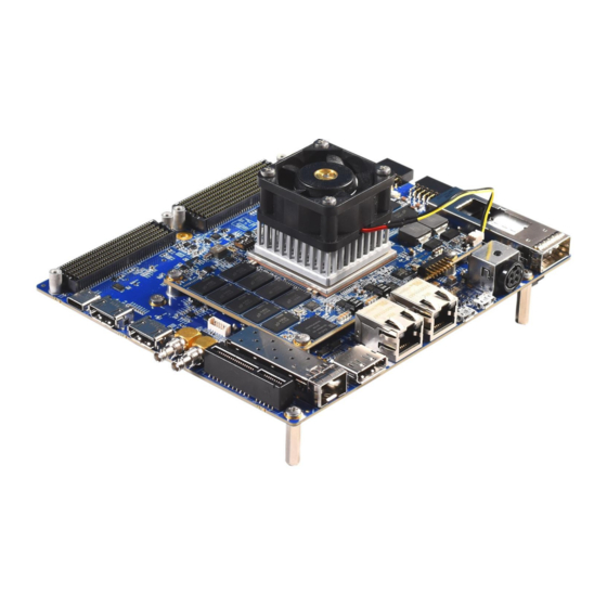
Page 108: Fan Sink Fixing Procedure On Som With Carrier Board
3.4.3 FAN Sink Fixing procedure on SOM with Carrier Board The Ultra-High-Performance Carrier board and Zynq Ultrascale+ SOM with Fan sink fixing procedure is shown below. Figure 42: Zynq Ultrascale+ SOM with Fan sink fixing procedure REL0.2 iWave Systems Technologies Pvt. Ltd. Page 108 of 110... -
Page 109: Ordering Information
ZU19EG (-3) MPSOC, 4GB PS DDR4 with ECC, Dual 4GB PL DDR4, 8GB Commercial EMMC - Development kit with Linux Note: For Development platform identification purpose, Product part number is pasted as Label with Barcode readable format. REL0.2 iWave Systems Technologies Pvt. Ltd. Page 109 of 110... - Page 110 Zynq-Ultrascale+ MPSoC (ZU11/17/19EG) SOM Development Platform Hardware User Guide REL0.2 iWave Systems Technologies Pvt. Ltd. Page 110 of 110...
Need help?
Do you have a question about the iW-RainboW-G35D and is the answer not in the manual?
Questions and answers