
Related Manuals for iWave iW-RainboW-G57M


Summary of Contents for iWave iW-RainboW-G57M
- Page 1 Versal AI Edge/Prime SOM Hardware User Guide iW-RainboW-G57M Versal AI Edge/Prime SOM Hardware User Guide Preliminary Information. Subject to change REL0.3 iWave Systems Technologies Pvt. Ltd. Page 1 of 63...
- Page 2 (or authorized to receive for the recipient), you are hereby notified that any disclosure, copying distribution or use of any of the information contained within this document is STRICTLY PROHIBITED. Thank you. “iWave Systems Tech. Pvt. Ltd.”...
- Page 3 No warranty of accuracy is given concerning the contents of the information contained in this publication. To the extent permitted by law no liability (including liability to any person by reason of negligence) will be accepted by iWave Systems, its subsidiaries or employees for any direct or indirect loss or damage caused by omissions from or inaccuracies in this document.
-
Page 4: Table Of Contents
2.6.3 Gigabit Ethernet Interface .......................... 40 2.6.4 RGMII/ULPI Interface ..........................41 2.6.5 SD/SDIO Interface ............................42 2.6.6 Debug UART Interface ..........................43 2.6.7 I2C Interface ..............................43 2.6.8 SPI Interface ..............................44 REL0.3 iWave Systems Technologies Pvt. Ltd. Page 4 of 63... - Page 5 3.2.3 Electrostatic Discharge ..........................58 Mechanical Characteristics ..........................59 3.3.1 Versal AI Edge SOM Mechanical Dimensions....................59 ORDERING INFORMATION ............................61 APPENDIX ................................62 Versal AI Edge SOM Development Platform ....................62 REL0.3 iWave Systems Technologies Pvt. Ltd. Page 5 of 63...
- Page 6 Table 25: PS IOMUX on Versal AI Edge SOM ............................51 Table 26: Power Input Requirement ..............................55 Table 27: Power Sequence Timing ...............................56 Table 28: Temperature Specification ..............................58 Table 29: Orderable Product Part Numbers ............................61 REL0.3 iWave Systems Technologies Pvt. Ltd. Page 6 of 63...
-
Page 7: Introduction
Purpose This document is the Hardware User Guide for the Versal AI Edge/Prime System on Module. This board is fully supported by iWave Systems Technologies Pvt. Ltd. This Guide provides detailed information on the overall design and usage of the Versal AI Edge/ Prime System on Module from a Hardware Systems perspective. - Page 8 Secure Digital Input Output System On Chip Serial Peripheral Interface System On Module Transmitter UART Universal Asynchronous Receiver/Transmitter ULPI UTMI+ Low Pin Interface Universal Serial Bus USB OTG USB On The Go REL0.3 iWave Systems Technologies Pvt. Ltd. Page 8 of 63...
-
Page 9: Terminology Description
Note: Signal Type does not include internal pull-ups or pull-downs implemented by the chip vendors and only includes the pull-ups or pull-downs implemented On-SOM. References • Versal AI Edge/Prime Technical Reference Manual • Versal AI Edge/Prime Device Overview • Versal AI Edge/Prime AC and DC characteristics REL0.3 iWave Systems Technologies Pvt. Ltd. Page 9 of 63... -
Page 10: Architecture And Design
¹ Versal Prime doesn’t support AI/ML Engine ² GTYP transceiver is not supported in VE2102 & VE2002 Preliminary Information Subject to Change Figure 1: Versal AI Edge/Prime SOM Block Diagram REL0.3 iWave Systems Technologies Pvt. Ltd. Page 10 of 63... -
Page 11: Versal Ai Edge Som Features
12 LVDS/24 Single ended signals from XP Bank 702 • 27 LVDS/54 Single ended signals from XP Bank 703 • 20 Single ended signals from HD Bank 302 • Synchronous Clock In/Out • 10MHz Reference Clock Input REL0.3 iWave Systems Technologies Pvt. Ltd. Page 11 of 63... - Page 12 GTYP Transceiver’s are not supported in VE2002 & VE2102 devices. In Versal AI Edge/Prime SOM, PL XP & HD IO BANKs supports variable IO voltage setting which configurable through software. REL0.3 iWave Systems Technologies Pvt. Ltd. Page 12 of 63...
-
Page 13: Versal Ai Edge
Figure 1: Versal AI Edge Simplified Block Diagram Note: Please refer the latest Versal AI Edge Datasheet & Technical Reference Manual for more details which may be revised from time to time. REL0.3 iWave Systems Technologies Pvt. Ltd. Page 13 of 63... - Page 14 PS, there is option in Versal to route IO peripheral interfaces to PL Bank I/O pins referred as EMIO (Extended MIO). Versal AI Edge PS Peripheral Pin mapping options between MIO & EMIO is shown below. REL0.3 iWave Systems Technologies Pvt. Ltd. Page 14 of 63...
-
Page 15: Table 3: Mio And Emio Pin Mapping Table
Also, Versal AI Edge supports 8 high-speed transceiver GTYP from Programmable Logic (PL). These transceivers are arranged in groups of four known as a transceiver Quad with Bank 103 & Bank 104 and supported line rate of 32 Gb/s. REL0.3 iWave Systems Technologies Pvt. Ltd. Page 15 of 63... -
Page 16: Soc Power
MIO or high-density I/O (HDIO) pins can be used by the SYSMON for measuring voltage levels external to the device. REL0.3 iWave Systems Technologies Pvt. Ltd. Page 16 of 63... -
Page 17: Versal Configuration Power & Status Leds
DONE_503 is output and its in open drain pin with weak internal pullup. This pin will become high when the boot sequence is complete. By default this pin is connected to VCC_1V8 through 4.7K. REL0.3 iWave Systems Technologies Pvt. Ltd. Page 17 of 63... -
Page 18: Versal Boot Mode Configuration
PS JTAG QSPI Note: SW4 boot media switch is assembled in the Carrier board to control SOM Boot media and SOM boot mode signals are connected to SW4 through Board-to-Board connector2. REL0.3 iWave Systems Technologies Pvt. Ltd. Page 18 of 63... -
Page 19: Clock Design
100MHz MSIO/SYS_SYNC_CLK_OUTp/ 3.3V, LVDS Clock input to A31 & A32 pin OUT5b MSIO/SYS_SYNC_CLK_OUTn of B2B1. PS Dedicated Input Oscillator 33.3333MHz MSIO/SYS_SYNC_CLK_INP 1.8V, LVCMOS Single ended reference clock /MSIO/SYS_SYNC_CLK_IN for PS. REL0.3 iWave Systems Technologies Pvt. Ltd. Page 19 of 63... -
Page 20: Versal Ai Edge/Prime Som Pmic's
PMIC’s Buck and LDO regulator is used for on SOM peripherals. Also, PMIC supports reset output and connected to Versal AI Edge (POR_B_503) for power on reset. Important Note: Every Power Off and On, The DA9062 PMIC work as initial OTP Setting REL0.3 iWave Systems Technologies Pvt. Ltd. Page 20 of 63... -
Page 21: Som Memory
SD0 controller of the Versal’s PS through MIO pins and operates at 1.8V Voltage level. This SD/SDIO controller supports eMMC 5.1 standard with up to 8bit HS400 mode. The eMMC Flash size can be expandable based on the availability of higher density eMMC Flash device. REL0.3 iWave Systems Technologies Pvt. Ltd. Page 21 of 63... -
Page 22: On Som Features
Figure 3: Fan Header Table 6: Fan Header Pinout Versal Versal Versal Signal Type/ Pin No Signal Name Description Pin Name Bank Pin No Termination VCC_5V O, 5V Power Supply Voltage. Power Ground. REL0.3 iWave Systems Technologies Pvt. Ltd. Page 22 of 63... -
Page 23: Board To Board Connector1
SOM as shown below. Number of Pins - 240 Connector Part Number - ADM6-60-01.5-L-4-2-A-TR from Samtech Mating Connector - ADF6-60-03.5-L-4-2-A-TR from Samtech Staking Height - 5mm Figure 4: Board to Board Connector 1 REL0.3 iWave Systems Technologies Pvt. Ltd. Page 23 of 63... -
Page 24: Table 7: : Board To Board Connector1 Pinout
XP_C23_LVDS703_L16P MSIO/SYS_SYNC_CLK_INN XP_C24_LVDS703_L15N XP_A24_LVDS703_L17N XP_B23_LVDS703_L16N XP_T23_LVDS702_L13P XP_M22_LVDS702_L15P XP_R24_LVDS702_L13N XP_M23_LVDS702_L15N XP_R23_LVDS702_L14P XP_L23_LVDS702_L16P XP_P24_LVDS702_L14N XP_K24_LVDS702_L16N XP_U23_LVDS702_L12P_GC XP_K23_LVDS702_L17P XP_T24_LVDS702_L12N_GC XP_J24_LVDS702_L17N XP_T21_LVDS702_L19P XP_N21_LVDS702_L21P XP_R22_LVDS702_L19N XP_M21_LVDS702_L21N XP_R21_LVDS702_L20P XP_K21_LVDS702_L22P XP_P22_LVDS702_L20N XP_L22_LVDS702_L22N XP_V21_LVDS702_L18P XP_J21_LVDS702_L23P XP_U22_LVDS702_L18N XP_J22_LVDS702_L23N MSIO/SYS_SYNC_CLK_OUTp REL0.3 iWave Systems Technologies Pvt. Ltd. Page 24 of 63... - Page 25 HD_D12_SE302_L3N HD_E14_SE302_L0N HD_D10_SE302_HDGC_L6P HD_B12_SE302_L9P HD_F11_SE302_L4P HD_C14_SE302_L1P HD_C10_SE302_HDGC_L6N HD_A13_SE302_L9N HD_E11_SE302_L4N HD_C13_SE302_L1N HD_D11_SE302_HDGC_L5P HD_B10_SE302_L7P HD_E13_SE302_L2P HD_C12_SE302_HDGC_L5N HD_A10_SE302_L7N HD_D14_SE302_L2N MSIO/10MHZ_REFCLK_IN *Power rails are highlighted in RED and Clock signals are highlighted in purple. REL0.3 iWave Systems Technologies Pvt. Ltd. Page 25 of 63...
-
Page 26: Interfaces
Clock input. IO, 1.5V XP Bank703 IO21 differential XP_B20_LVDS703_L21 IO_L21P_XCC_N7P0 positive or single ended I/O. _703 XP_C21_LVDS703_L21 IO_L21N_XCC_N7P1 IO, 1.5V XP Bank703 IO21 differential _703 negative or single ended I/O. REL0.3 iWave Systems Technologies Pvt. Ltd. Page 26 of 63... - Page 27 I/O. _703 XP_C27_LVDS703_L5P IO_L5P_N1P4_703 IO, 1.5V XP Bank703 IO5 differential positive or single ended I/O. XP_B28_LVDS703_L5N IO_L5N_N1P5_703 IO, 1.5V XP Bank703 IO5 differential negative or single ended I/O. REL0.3 iWave Systems Technologies Pvt. Ltd. Page 27 of 63...
- Page 28 IO_L20N_N6P5_703 negative or single ended I/O. XP_H23_LVDS703_L12 IO_L12P_GC_XCC_N IO, 1.5V XP Bank703 IO12 differential P_GC 4P0_703 positive or single ended I/O. Same pin can be used as Global Clock input. REL0.3 iWave Systems Technologies Pvt. Ltd. Page 28 of 63...
- Page 29 I/O. *IO Type of IOs originating from Versal AI Edge SoC is configurable. Hence for exact IO type configuration options, refer Xilinx Versal AI Edge datasheet. REL0.3 iWave Systems Technologies Pvt. Ltd. Page 29 of 63...
-
Page 30: Ios - Xpio Bank 702
I/O. XP_R22_LVDS702_L19N IO_L19N_N6P3_M0P IO, 1.5V XP Bank702 IO19 differential 147_702 negative or single ended I/O. XP_R21_LVDS702_L20P IO_L20P_N6P4_M0P IO, 1.5V XP Bank702 IO20 differential positive or single ended I/O. 148_702 REL0.3 iWave Systems Technologies Pvt. Ltd. Page 30 of 63... - Page 31 I/O _M0P139_702 XP_L23_LVDS702_L16P IO_L16P_N5P2_M0P IO, 1.5V XP Bank702 IO16 differential 140_702 positive or single ended I/O. XP_K24_LVDS702_L16N IO_L16N_N5P3_M0P IO, 1.5V XP Bank702 IO16 differential 141_702 negative or single ended I/O REL0.3 iWave Systems Technologies Pvt. Ltd. Page 31 of 63...
- Page 32 I/O. *IO Type of IOs originating from Versal AI Edge SoC is configurable. Hence for exact IO type configuration options, refer Xilinx Versal AI Edge datasheet. REL0.3 iWave Systems Technologies Pvt. Ltd. Page 32 of 63...
-
Page 33: Ios - Hd Bank 302
HD_C14_SE302_L1P IO_L1P_302 IO, 1.8V HD Bank302 IO1 single ended I/O. HD_C13_SE302_L1N IO_L1N_302 IO, 1.8V HD Bank302 IO1 single ended I/O. IO, 1.8V HD Bank302 IO2 single ended I/O. HD_E13_SE302_L2P IO_L2P_302 REL0.3 iWave Systems Technologies Pvt. Ltd. Page 33 of 63... -
Page 34: Power Control Output
B8, B17, B24, B33, B40, B49, B50, B53, B54, B57, B58, C8, C17, C24, C33, C40, C51, C52, C55, C56, C59, C60, D8, D17, D24, D33, D40, D49, D50, D53, D54, D57, D58 REL0.3 iWave Systems Technologies Pvt. Ltd. Page 34 of 63... -
Page 35: Board To Board Connector2
SOM as shown below. Number of Pins - 240 Connector Part Number - ADM6-60-01.5-L-4-2-A-TR from Samtech Mating Connector - ADF6-60-03.5-L-4-2-A-TR from Samtech Staking Height - 5mm Figure 5: Board to Board Connector 2 REL0.3 iWave Systems Technologies Pvt. Ltd. Page 35 of 63... -
Page 36: Table 12: Board To Board Connector2 Pinout
(LPD_MIO12_502) USB_OTG_DP USB_OTG_ID C17 GEM1_TXD0(LPD_MIO13_5 SPI1_SI(PMC_MIO11_500) VBUS_USB C18 GEM1_TXD1(LPD_MIO14_5 SPI1_S0(PMC_MIO10_500) GPHY_ATXRXM GPHY_ACTIVITY_LED1 C19 GEM1_TXD2(LPD_MIO15_5 SPI1_CS2(PMC_MIO7_500) GPHY_ATXRXP GPHY_LINK_LED2 C20 GEM1_TXD3(LPD_MIO16_5 SPI1_CS1(PMC_MIO8_500) GPIO(PMC_MIO27_501) GEM1_TX_CTL(LPD_MIO17 SPI1_CS0(PMC_MIO9_500) _502) GPHY_BTXRXM GPHY_BTXRXP SD1_CLK GEM1_RX_CLK(LPD_MIO18 (PMC_MIO26_501) _502) REL0.3 iWave Systems Technologies Pvt. Ltd. Page 36 of 63... - Page 37 GTYP_RXN0_103 GTYP_RXN2_103 GTYP_TXP1_103 GTYP_TXP3_103 GTYP_TXN1_103 GTYP_TXN3_103 GTYP_TXP0_103 GTYP_TXP2_103 GTYP_TXN0_103 GTYP_TXN2_103 GTYP_REFCLK0P_104 B2B_GTYP_REFCLK1P_104 GTYP_REFCLK0N_104 B2B_GTYP_REFCLK1N_104 GTYP_RXP0_104 GTYP_RXP2_104 GTYP_RXN0_104 GTYP_RXN2_104 GTYP_RXP1_104 GTYP_RXP3_104 GTYP_RXN1_104 GTYP_RXN3_104 GTYP_TXP0_104 GTYP_TXP2_104 GTYP_TXN0_104 GTYP_TXN2_104 GTYP_TXP1_104 GTYP_TXP3_104 GTYP_TXN1_104 GTYP_TXN3_104 REL0.3 iWave Systems Technologies Pvt. Ltd. Page 37 of 63...
- Page 38 Versal AI Edge SOM Hardware User Guide B2B-2 Signal Name B2B- Signal Name B2B-2 Pin Signal Name B2B-2 Signal Name 2 Pin *Power rails are highlighted in RED and Clock signals are highlighted in purple. REL0.3 iWave Systems Technologies Pvt. Ltd. Page 38 of 63...
-
Page 39: Ps Interfaces
USB OTG ID input for USB host or USB_OTG_ID device detection. O, 3.3V USB active high power enable output USB_PWR_EN CMOS to control external USB Vbus. VBUS_USB I, 5V Power USB VBUS for VBUS monitoring. REL0.3 iWave Systems Technologies Pvt. Ltd. Page 39 of 63... -
Page 40: Gigabit Ethernet Interface
IO, GBE Gigabit Ethernet differential pair 4 GPHY_DTXRXM negative. O, GBE Gigabit Ethernet Activity LED (Active GPHY_ACTIVITY_LED1 High). O, GBE Gigabit Ethernet 1000Mbps Link GPHY_LINK_LED2 status LED (Active High). REL0.3 iWave Systems Technologies Pvt. Ltd. Page 40 of 63... -
Page 41: Rgmii/Ulpi Interface
GEM1 RGMII Receive DATA2. 2_502) GEM1_RX_CTL(LPD_MI LPD_MIO23_502 I, 1.8V LVCMOS GEM1 RGMII Receive control. O23_502) GEM1_MDC(LPD_MIO2 LPD_MIO24_502 O, 1.8V LVCMOS MDC Clock Output 4_502) LPD_MIO25_502 IO, 1.8V MDIO Data In/Out GEM1_MDIO(LPD_MIO 25_502) LVCMOS REL0.3 iWave Systems Technologies Pvt. Ltd. Page 41 of 63... -
Page 42: Sd/Sdio Interface
PMC_MIO31_501 501 AD6 O31_501) 10K PU SD1_DATA2(PMC_MI IO, 1.8V LVCMOS/ SD1 DATA2. PMC_MIO32_501 501 AB6 O32_501) 10K PU IO, 1.8V LVCMOS/ SD1 DATA3. SD1_DATA3(PMC_MI PMC_MIO33_501 501 AA6 10K PU O33_501) REL0.3 iWave Systems Technologies Pvt. Ltd. Page 42 of 63... -
Page 43: Debug Uart Interface
Pin No Signal Name Bank Termination I2C_SCL(PMC_MIO5 PMC_MIO50_501 AB10 O, 1.8V OD/ I2C Serial Clock. 0_501) 4.7K PU I2C_SDA(PMC_MIO PMC_MIO51_501 AA10 IO, 1.8V OD/ I2C Serial Data. 51_501) 4.7K PU REL0.3 iWave Systems Technologies Pvt. Ltd. Page 43 of 63... -
Page 44: Spi Interface
SPI1_S0(PMC_MIO PMC_MIO10_500 10_500) SPI1_CS2(PMC_MI PMC_MIO7_500 O, 1.8V LVCMOS SPI chip select2. O7_500) SPI1_CS1(PMC_MI PMC_MIO8_500 O, 1.8V LVCMOS SPI chip select1. O8_500) O, 1.8V LVCMOS SPI1_CS0(PMC_MI PMC_MIO9_500 SPI chip select0. O9_500) REL0.3 iWave Systems Technologies Pvt. Ltd. Page 44 of 63... -
Page 45: Can Fd Interface
JTAG_TDI TDI_503 AG10 I, 1.8V LVCMOS/ JTAG Test Data Input. 4.7K JTAG_TDO TDO_503 O, 1.8V LVCMOS JTAG Test Data Output. JTAG_TMS TMS_503 I, 1.8V LVCMOS/ JTAG Test Mode Select. 4.7K REL0.3 iWave Systems Technologies Pvt. Ltd. Page 45 of 63... -
Page 46: Interfaces
GTYP Bank103 channel0 High speed differential receiver positive. GTYP_RXN0_103 GTYP_RXN0_103 I, DIFF GTYP Bank103 channel0 High speed differential receiver negative. GTYP_TXP1_103 O, DIFF GTYP Bank103 channel1 High speed GTYP_TXP1_103 differential transmitter positive. REL0.3 iWave Systems Technologies Pvt. Ltd. Page 46 of 63... - Page 47 GTYP Bank104 channel1 High speed differential transmitter negative. GTYP_RXP1_104 GTYP_RXP1_104 I, DIFF GTYP Bank104 channel1 High speed differential receiver positive. I, DIFF GTYP Bank104 channel1 High speed GTYP_RXN1_104 GTYP_RXN1_104 differential receiver negative. REL0.3 iWave Systems Technologies Pvt. Ltd. Page 47 of 63...
-
Page 48: Power, Reset & Control Signals
The Versal AI Edge SOM support an optional reference clock 1 input for GTYP Bank 103 & 104 from board-to-board connector 2 with a pins of C31, C32, D31, D42. For more details on Power pins on Board-to-Board Connector2, refer the below table. REL0.3 iWave Systems Technologies Pvt. Ltd. Page 48 of 63... -
Page 49: Table 24: Board To Board Connector2 Control & Power Pins
Optional Reference clock1 for K1P_104 KP1_104 GTYP Bank 104 B2B_GTYP_REFCL GTYP_REFCL I, DIFF Optional Reference clock1 for K1N_104 KN1_104 GTYP Bank 104 VRTC_3V0 I, 3V Power 3V backup coin cell input for RTC. REL0.3 iWave Systems Technologies Pvt. Ltd. Page 49 of 63... - Page 50 C37, C38, C41, C42, C45, C46, C49, C50, C53, C54,C57, C58, D6, D7, D15, D22, D31, D32, D35, D36, D39, D40, D43, D44, D47, D48, D51, D52, D55, D56, D59, REL0.3 iWave Systems Technologies Pvt. Ltd. Page 50 of 63...
-
Page 51: Versal Ai Edge Ps Pin Multiplexing On Board To Board Connectors
QSPI0_IO[ QSPI0_IO[ OSPI_IO[2 OSPI_IO[2 SD1/EMM SD1/EMM SD1/EMM SD1/EMM SD1/EMM SD1/EMM PMC_I2C CANFD1_ UART SPI0_SS0_ LPD_I2C0 SWDT0_I 3_500 PIO3 C1: CMD C1_CMD C1_CMD C1: CMD C1_CMD C1_CMD _SDA 0_RTS_B _SDA 2_WAVE REL0.3 iWave Systems Technologies Pvt. Ltd. Page 51 of 63... - Page 52 _502 0_RTS_B _SDA 2_WAVE LPD_MIO4 LPD_GP GEM0_TXD[ CANFD1_ UART SPI0_MSI LPD_I2C1 SWDT0_ TTC 1_CLK _502 1_TXD _SCL LPD_MIO5 LPD_GP GEM0_TX_ CANFD1_ UART SPI0_MO LPD_I2C1 SWDT0_ _502 CTRL 1_RXD _SDA 1_WAVE REL0.3 iWave Systems Technologies Pvt. Ltd. Page 52 of 63...
- Page 53 _SDA 1_RXD _SDA 1_WAVE PMC_MIO PMC_G SD1/EMM SD1/EMM SD1/EMM SD1/EMM SD1/EMM SMAP_IO[ GEM0_RX CANFD1_ UART SPI1_SCLK LPD_I2C1 SWDT1_C TTC 0_CLK 32_501 PIO32 C1_DATA[ C1_DATA[ C1_DATA[ C1_DATA[ C1_DATA[ _CLK 1_RTS_B _SCL REL0.3 iWave Systems Technologies Pvt. Ltd. Page 53 of 63...
- Page 54 _CLK DIO_CLK DIO_CLK _SCL LPD_MIO2 LPD_GP GEM0_MDI GEM0_M GEM_TSU GEM0_M GEM1_M CANFD1_ LPD_I2C1 5_502 IO25 O_DATA DIO_DAT _CLK DIO_DAT DIO_DAT _SDA JTAG TCK_503 JTAG_TCK TDI_503 JTAG_TDI TDO_503 JTAG_TDO TMS_503 JTAG_TMS REL0.3 iWave Systems Technologies Pvt. Ltd. Page 54 of 63...
-
Page 55: Technical Specification
²Versal AI Edge SOM uses this voltage as backup power source to PMIC RTC when VCC_5V is off. This is an optional power and required only if RTC functionality is used. REL0.3 iWave Systems Technologies Pvt. Ltd. Page 55 of 63... -
Page 56: Power Input Sequencing
SOMPWR_EN fall time to VCC_5V fall time ≥ 0 ms VCC_5V fall time to VRTC_3V0 fall time ≥ 0 ms ¹ VRTC_3V0 is the RTC Battery backup supply. This is an optional power. REL0.3 iWave Systems Technologies Pvt. Ltd. Page 56 of 63... -
Page 57: Power Consumption
Versal AI Edge SOM Hardware User Guide 3.1.3 Power Consumption REL0.3 iWave Systems Technologies Pvt. Ltd. Page 57 of 63... -
Page 58: Environmental Characteristics
3.2.3 Electrostatic Discharge iWave’s Versal AI Edge SOM is sensitive to electro static discharge and so high voltages caused by static electricity could damage some of the devices on board. It is packed with necessary protection while shipping. Do not open or use the SOM except at an electrostatic free workstation. -
Page 59: Mechanical Characteristics
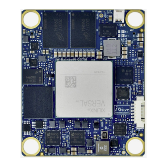
Versal AI Edge SOM PCB size is 50mm x 60mm x 1.83mm. SOM mechanical dimension is shown below. Figure 7: Mechanical dimension of Versal AI Edge SOM SOM - Top View REL0.3 iWave Systems Technologies Pvt. Ltd. Page 59 of 63... -
Page 60: Figure 8: Mechanical Dimension Of Versal Ai Edge Som - Bottom View
3.5mm and bottom side maximum height component is Board to Board connector 1 & 2 (4.1mm). Please refer the below figure which gives height details of Versal SOM. Figure 9: Top and Bottom Maximum Heighted Component REL0.3 iWave Systems Technologies Pvt. Ltd. Page 60 of 63... -
Page 61: Ordering Information
The below table provides the standard orderable part numbers for different Versal AI Edge SOM variations. Please contact iWave for orderable part number of higher RAM memory size or Flash memory size SOM configurations. Also, if the desired part number is not listed in below table or if any custom configuration part number is required, please contact iWave. -
Page 62: Appendix
Versal AI Edge SOM Development Platform iWave Systems supports iW-RainboW-G57M– Versal AI Edge SOM Development Platform which is targeted for quick validation of Versal based SOM. iWave's Versal AI Edge Development Board incorporates Versal AI Edge SOM and High-performance Carrier board with complete BSP support. -
Page 63: Iwave Systems Technologies Pvt. Ltd
Versal AI Edge SOM Hardware User Guide REL0.3 iWave Systems Technologies Pvt. Ltd. Page 63 of 63...
Need help?
Do you have a question about the iW-RainboW-G57M and is the answer not in the manual?
Questions and answers