
Related Manuals for Xilinx FMC XM105


Summary of Contents for Xilinx FMC XM105
- Page 1 FMC XM105 Debug Card User Guide UG537 (v1.2) September 24, 2010 Downloaded from Elcodis.com electronic components distributor...
-
Page 2: Revision History
Xilinx. Xilinx expressly disclaims any liability arising out of your use of the Documentation. Xilinx reserves the right, at its sole discretion, to change the Documentation without notice at any time. Xilinx assumes no obligation to correct any errors contained in the Documentation, or to advise you of any corrections or updates. -
Page 3: Table Of Contents
Related Xilinx Documents ........ - Page 4 HW-FMC-105-DEBUG User Guide UG537 (v1.2) September 24, 2010 Downloaded from Elcodis.com electronic components distributor...
-
Page 5: Preface: About This Guide
Preface About This Guide This document describes the FMC XM105 debug card (HW-FMC-XM105-G), referred to as the XM105 in this guide. Xilinx FMC-supported evaluation (carrier) boards are referred to simply as boards in this guide. Guide Contents This manual contains the following chapters: •... - Page 6 Preface: About This Guide www.xilinx.com FMC XM105 Debug Card User Guide UG537 (v1.2) September 24, 2010 Downloaded from Elcodis.com electronic components distributor...
-
Page 7: Chapter 1: Xm105
Board Technical Description are combined within this document. Related Xilinx Documents Prior to using the XM105 users should be familiar with Xilinx resources. See the following locations for additional documentation on Xilinx tools and solutions: • ISE: www.xilinx.com/ise •... -
Page 8: Quick Start
EK-V6-ML605-G Notes: While every effort has been made to comply with the FPGA Mezzanine Card Specification, Xilinx cannot claim nor assume full compliance with the FMC/VITA-57-1 specification. Consequently, Xilinx cannot claim nor support the usage of the XM105 on any other FMC (VITA-57.1) board. -
Page 9: System Setup
XM105. Hand tighten the two mounting screws to the bottom of the board. Turn the attached board and XM105 unit over so that the Xilinx FPGA is visible. Connect the input power source to the board. Turn the board power input switch to The system is now ready for use. -
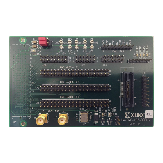
Page 10: Board Technical Description
1 x 9 JTAG 2 Kb Power Good EEPROM LEDs Requires board with FMC HPC support. UG537_02_110509 Figure 1-2: XM105 Block Diagram www.xilinx.com FMC XM105 Debug Card User Guide UG537 (v1.2) September 24, 2010 Downloaded from Elcodis.com electronic components distributor... -
Page 11: Detailed Description
J16: 6 pin x 2 row male header 6-pin header J15: 6 pin x 1 row male header User LEDS Four user LEDS FMC XM105 Debug Card User Guide www.xilinx.com UG537 (v1.2) September 24, 2010 Downloaded from Elcodis.com electronic components distributor... - Page 12 Notes: 1. Available only with FMC HPC board interfaces. Xilinx Virtex-6 FPGA ML605 evaluation board provides one FMC LPC and one FMC HPC interface. Xilinx Spartan-6 FPGA SP601 and SP605 evaluation boards provide a single FMC LPC interface. www.xilinx.com FMC XM105 Debug Card User Guide UG537 (v1.2) September 24, 2010...
-
Page 13: Vita 57.1 Fmc Hpc Connector J17
Board Technical Description 1. VITA 57.1 FMC HPC Connector J17 This connector provides the interface to the board containing the Xilinx FPGA. The XM105 uses Samtec FMC HPC connector part number ASP-134488-01. The XM105 connector mates with a FMC LPC connector or an FMC HPC connector on Xilinx boards. - Page 14 IIC_SCL_MAIN FMC_LA23_N EEPROM, Si570 IIC_SDA_MAIN FMC_LA26_P EEPROM FMC_LA26_N VCC12 FMC_TCK VCC12 FMC_TDI VCC3V3 FMC_TDO VCC3V3_AUX FMC_TMS No connect EEPROM VCC3V3 VCC3V3 VCC3V3 www.xilinx.com FMC XM105 Debug Card User Guide UG537 (v1.2) September 24, 2010 Downloaded from Elcodis.com electronic components distributor...
- Page 15 FMC_HB21_P FMC_HB16_N FMC_HB21_N FMC_HB20_P VADJ FMC_HB20_N VADJ CLK1_M2C_P No connect Tied to GND CLK1_M2C_N (PRSNT_M2C_L) FMC_LA00_CC_P J1, P1 CLK0_M2C_P Si570 FMC_LA00_CC_N CLK0_M2C_N FMC XM105 Debug Card User Guide www.xilinx.com UG537 (v1.2) September 24, 2010 Downloaded from Elcodis.com electronic components distributor...
- Page 16 FMC_LA22_N FMC_LA19_N FMC_LA25_P FMC_LA21_P FMC_LA25_N FMC_LA21_N FMC_LA29_P FMC_LA24_P FMC_LA29_N FMC_LA24_N FMC_LA31_P FMC_LA28_P FMC_LA31_N FMC_LA28_N FMC_LA33_P FMC_LA30_P FMC_LA33_N FMC_LA30_N VADJ FMC_LA32_P FMC_LA32_N VADJ www.xilinx.com FMC XM105 Debug Card User Guide UG537 (v1.2) September 24, 2010 Downloaded from Elcodis.com electronic components distributor...
- Page 17 FMC_HA23_N FMC_HB01_N FMC_HB00_CC_P FMC_HB07_P FMC_HB00_CC_N FMC_HB07_N FMC_HB06_CC_P FMC_HB11_P FMC_HB06_CC_N FMC_HB11_N FMC_HB10_P FMC_HB15_P FMC_HB10_N FMC_HB15_N FMC_HB14_P FMC_HB18_P FMC_HB14_N FMC_HB18_N FMC_HB17_CC_P VADJ FMC_HB17_CC_N VADJ FMC XM105 Debug Card User Guide www.xilinx.com UG537 (v1.2) September 24, 2010 Downloaded from Elcodis.com electronic components distributor...
-
Page 18: Connector J6 6-Pin Header
Chapter 1: XM105 See the Xilinx board user guides and schematics for a description of features provided by LPC and/or HPC interfaces contained on the board, including power supply specifications, FPGA banking connectivity, and FPGA pin assignments. • For SP601 LPC interface, see... -
Page 19: Connector J5 Fmc Jtag
FMC HPC JTAG signals. This interface is not intended to provide a means to program the FPGA on the board. See the Xilinx board user guide for details of board JTAG interface support of FMC mezzanine cards. Connections between the mezzanine FMC HPC and... -
Page 20: Connector J23
Notes: 1. Available only when connected to board with FMC HPC interface support. 2. These pins are not connected on the Xilinx ML605 FMC HPC board interface. 6. Connector J16 This 12-position connector provides an interface from the XM105 to 12 single-ended signals on the board’s FMC LPC or FMC HPC interface. -
Page 21: Connector J15
J17 Pin (Even Pins) FMC_HB00_CC _P FMC_HB10_P FMC_HB00_CC _N FMC_HB10_N FMC_HB01_P FMC_HB11_P FMC_HB01_N FMC_HB11_N FMC_HB02_P FMC_HB12_P FMC_HB02_N FMC_HB12_N FMC_HB03_P FMC_HB13_P FMC_HB03_N FMC_HB13_N FMC XM105 Debug Card User Guide www.xilinx.com UG537 (v1.2) September 24, 2010 Downloaded from Elcodis.com electronic components distributor... - Page 22 FMC_HB19_P FMC_HB09_N FMC_HB19_N Notes: 1. Signal names with “_CC_” can be connected to FPGA clock capable pins on the board. See Xilinx board user guides for additional information. www.xilinx.com FMC XM105 Debug Card User Guide UG537 (v1.2) September 24, 2010 Downloaded from Elcodis.com...
-
Page 23: Connector J1
FMC_LA19_P FMC_LA09_N FMC_LA19_N Notes: 1. Signal names with “_CC_” can be connected to FPGA clock capable pins on the board. See Xilinx board user guides for additional information. FMC XM105 Debug Card User Guide www.xilinx.com UG537 (v1.2) September 24, 2010 Downloaded from Elcodis.com... -
Page 24: Connector J3
FMC_HA19_P FMC_HA09_N FMC_HA19_N Notes: 1. Signal names with “_CC_” can be connected to FPGA clock capable pins on the board. See Xilinx board user guides for additional information. www.xilinx.com FMC XM105 Debug Card User Guide UG537 (v1.2) September 24, 2010 Downloaded from Elcodis.com... -
Page 25: Mictor Connector P1
Notes: 1. Mictor JTAG signals are available on 9-position connector J19. 2. Signal names with “_CC_” may be connected to FPGA clock capable pins on the board. See Xilinx board user guides for additional information. FMC XM105 Debug Card User Guide www.xilinx.com... -
Page 26: Connector J19
Table 1-13: Connector J19 Pin Assignments Mictor P1 Signal Name Connector Connector 3.3V – GROUND – – MICTOR_TCK – MICTOR_TDO MICTOR_TDI – MICTOR_TMS www.xilinx.com FMC XM105 Debug Card User Guide UG537 (v1.2) September 24, 2010 Downloaded from Elcodis.com electronic components distributor... -
Page 27: Clocks
A pair of differential SMA connectors can be utilized to provide a high-precision differential clock or a single-ended clock to the board. Virtex-6 FPGA and Spartan-6 FPGA devices require single-ended clocks on the “P” input of an IOB pair. See Xilinx FPGA documentation for additional information. -
Page 28: Kb Eeprom
E0 and E1. As shown in Table 1-16, Xilinx boards provide GA0 and GA1 signal strapping to 3.3V and GND signals, which creates a different E0 and E1 chip enable decode on the E1 and E0 inputs of the EEPROM. -
Page 29: Power Good Leds
FPGA input. Connection to ground is only used to signal power not good from the XM105 to the board. There are no power supplies on this XM105. By default, the connector is left open. See Xilinx board user guides and schematics for additional information. •... - Page 30 Chapter 1: XM105 www.xilinx.com FMC XM105 Debug Card User Guide UG537 (v1.2) September 24, 2010 Downloaded from Elcodis.com electronic components distributor...
Need help?
Do you have a question about the FMC XM105 and is the answer not in the manual?
Questions and answers