Table of Contents
Advertisement
Quick Links
Advertisement
Table of Contents

Related Manuals for Xilinx FMC XM101 LVDS QSE


Summary of Contents for Xilinx FMC XM101 LVDS QSE
- Page 1 FMC XM101 LVDS QSE Card User Guide UG538 (v1.1) September 24, 2010...
-
Page 2: Revision History
Xilinx. Xilinx expressly disclaims any liability arising out of your use of the Documentation. Xilinx reserves the right, at its sole discretion, to change the Documentation without notice at any time. Xilinx assumes no obligation to correct any errors contained in the Documentation, or to advise you of any corrections or updates. -
Page 3: Table Of Contents
..........21 6. M24C02 2 Kb IIC EEPROM FMC XM101 User Guide www.xilinx.com UG538 (v1.1) September 24, 2010... - Page 4 FMC XM101 User Guide UG538 (v1.1) September 24, 2010...
-
Page 5: Preface: About This Guide
Information about the latest VITA 57 FMC Specification is located at: • www.vita.com/fmc.html The XM101 can be used with Xilinx FMC high pin count (HPC) boards and, with limited functionality, FMC low pin count (LPC) boards. Board documentation, schematics and PCB design files are available at www.xilinx.com/fmc. - Page 6 Preface: About This Guide www.xilinx.com FMC XM101 User Guide UG538 (v1.1) September 24, 2010...
-
Page 7: Chapter 1: Xm101
EK-V6-ML605-G Notes: While every effort has been made to comply with the FPGA Mezzanine Card Specification, Xilinx cannot claim nor assume full compliance with the FMC/VITA-57-1 specification. Consequently, Xilinx cannot claim nor support the usage of the XM101 on any other FMC (VITA-57.1) board. -
Page 8: Package Contents
XM101. Hand tighten the two mounting screws to the bottom of the board. Turn the ML605 and attached XM101 boards over such that the Xilinx FPGA is visible. Connect the input power source to the ML605 board. Turn the ML605 board power input switch to ON. -
Page 9: Technical Support
UG538_01_011210 Figure 1-1: Installation of XM101 to ML605 Board FMC HPC Connector Technical Support Xilinx offers technical support for this product only when used in conjunction with boards listed in Table 1-1. For assistance with the XM101 and other Xilinx boards, contact Xilinx for technical support at www.xilinx.com/support. -
Page 10: Xm101 Board Technical Description
IIC bus implemented in the FMC HPC interface, enabling the board’s FPGA to program the clock circuitry on the XM101. A 2-Kb serial IIC EEPROM is also connected to the IIC interface of the board, providing non-volatile storage. www.xilinx.com FMC XM101 User Guide UG538 (v1.1) September 24, 2010... -
Page 11: Detailed Description
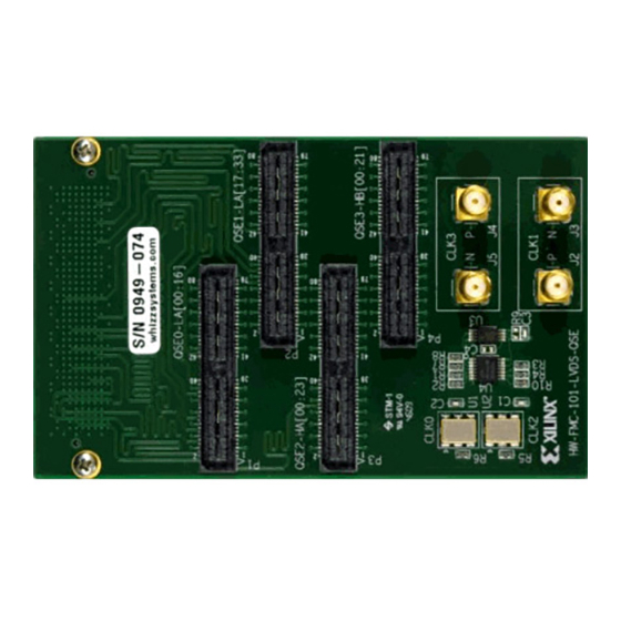
12. For full functionality, the XM101 must be installed on a board FMC connector supporting high pin count interfaces. X-Ref Target - Figure 1-3 UG538_03_011210 Figure 1-3: XM101 Features FMC XM101 User Guide www.xilinx.com UG538 (v1.1) September 24, 2010... - Page 12 Connections and J5 are connected to CLK3_M2C_P and N, respectively. U3: IIC compatible electrically erasable M24C02 2Kb IIC programmable memory (EEPROM) with 2 Kb EEPROM (256 bytes) of non-volatile storage. www.xilinx.com FMC XM101 User Guide UG538 (v1.1) September 24, 2010...
-
Page 13: Vita 57.1 Fmc Hpc Connector J1
This connector interfaces to the board containing the Xilinx FPGA and mating FMC connector. The XM101 uses Samtec FMC HPC connector part number ASP-134488-01. See Xilinx board user guides and schematics for a description of features provided by HPC interfaces contained on the board, including power supply specifications, FPGA banking connectivity, and FPGA pin assignments. - Page 14 LA04_P LA05_P LA04_N LA05_N LA06_P LA07_P LA06_N LA07_N LA08_P LA09_P LA08_N LA09_N LA00_CC_P LA01_CC_P LA00_CC_N LA01_CC_N LA10_P LA11_P LA10_N LA11_N LA12_P LA13_P LA12_N LA13_N LA14_P LA15_P LA14_N LA15_N LA16_P LA16_N www.xilinx.com FMC XM101 User Guide UG538 (v1.1) September 24, 2010...
- Page 15 LA21_P LA22_P LA21_N LA22_N LA23_P LA24_P LA23_N LA24_N LA25_P LA26_P LA25_N LA26_N LA17_CC_P LA18_CC_P LA17_CC_N LA18_CC_N LA27_P LA28_P LA27_N LA28_N LA29_P LA30_P LA29_N LA30_N LA31_P LA32_P LA31_N LA32_N LA33_P LA33_N FMC XM101 User Guide www.xilinx.com UG538 (v1.1) September 24, 2010...
- Page 16 HA00_CC_N HA01_CC_N HA10_P HA11_P HA10_N HA11_N HA12_P HA13_P HA12_N HA13_N HA14_P HA15_P HA14_N HA15_N HA16_P HA17_CC_P HA16_N HA17_CC_N HA18_P HA19_P HA18_N HA19_N HA20_P HA21_P HA20_N HA21_N HA22_P HA23_P HA22_N HA23_N www.xilinx.com FMC XM101 User Guide UG538 (v1.1) September 24, 2010...
- Page 17 HB14_P HB15_P HB14_N HB15_N HB16_P HB17_CC_P HB16_N HB17_CC_N HB18_P HB19_P HB18_N HB19_N HB20_P HB21_P HB20_N HB21_N Notes: 1. The ML605 board FMC HPC connector J64 does not support these signals FMC XM101 User Guide www.xilinx.com UG538 (v1.1) September 24, 2010...
-
Page 18: Pca9543 Iic Bus Switch
A1 and A0 of the PCA9543 component. Xilinx boards provide GA0 and GA1 signal strapping to 3.3V and GND signals creating different A0 and A1 address decodes on the PCA9543. - Page 19 XM101 Board Technical Description PCA9543 Device Select Code as well as specific Device Code Select address when the XM101 is connected to a Xilinx board as defined in Table 1-1, page Table 1-8: PCA9543 IIC Switch Device Select Code Bit 7:4 Device...
-
Page 20: Silicon Labs Si570 Clock Sources
The U1 and U2 Si570 output clocks to J1 FMC HPC connections are shown in Table 1-12. Table 1-12: Si570 to FMC HPC Connections J1 FMC Si570 Connector Net Name Pin Number Pin Number CLK0_M2C_P U1.4 CLK0_M2C_N U1.5 CLK2_M2C_P U2.4 CLK2_M2C_N U2.5 www.xilinx.com FMC XM101 User Guide UG538 (v1.1) September 24, 2010... -
Page 21: Sma Clock Connections
M24C02 component enables E0 and E1. Xilinx boards provide GA0 and GA1 signal strapping to 3.3V and GND signals creating different E0 and E1 chip enable decodes on the E1 and E0 inputs of the EEPROM. - Page 22 Chapter 1: XM101 www.xilinx.com FMC XM101 User Guide UG538 (v1.1) September 24, 2010...
- Page 23 Mouser Electronics Authorized Distributor Click to View Pricing, Inventory, Delivery & Lifecycle Information: Xilinx HW-FMC-XM101-G...
Need help?
Do you have a question about the FMC XM101 LVDS QSE and is the answer not in the manual?
Questions and answers