Table of Contents
Advertisement
Quick Links
Advertisement
Table of Contents

Related Manuals for Advantech SOM-ETX Series


Summary of Contents for Advantech SOM-ETX Series
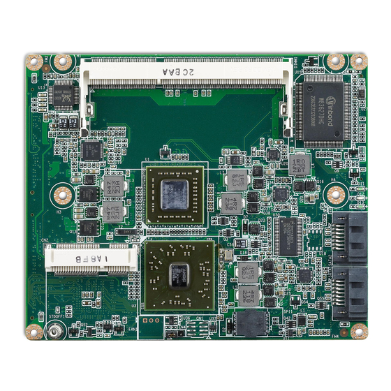
- Page 1 Advantech SOM-ETX Series System On Modules Design Guide Version 1.0...
- Page 2 Advantech SOM-ETX Design Guide Notices The copyright on this user manual remains with Advantech Co., Ltd. No part of this user manual may be transmitted, reproduced, or changed. Other companies’ product names that may be used herein remain the property of their respective owners.
-
Page 3: Table Of Contents
Advantech SOM-ETX Design Guide Table of Contents Chapter 1 Introduction....................9 Terminology.....................9 Table 1.1 Conventions and Terminology ........9 Referenced Documents.................10 Table 1.2 Referenced Documents ..........10 Chapter 2 SOM-ETX Overview ................11 Overview....................11 Figure 2-1 ..................11 Figure 2-2 ..................11 Figure 2-3 ..................12 Specifications ..................13 Table 2.1 SOM-4481 Specifications ..........13... - Page 4 Table 2.36 SOM-4450 DMA Resources ........40 Table 2.37 SOM-4450 Memory Map ..........40 Table 2.38 SOM-4450 I/O Map............41 PCI Routing ...................42 Table 2.40 Advantech SOM-ETX Modules PCI Routing .....42 DC Specifications ..................42 2.5.1 Power Consumption ..............42 Table 2.41 Power Consumption (SOM-4481)......42 Table 2.42 Power Consumption (SOM-4475)......43...
- Page 5 Advantech SOM-ETX Design Guide 2.6.7 Ethernet AC Spec.................50 2.6.8 TV-Out Bus AC Spec..............50 2.6.9 I2C AC Spec.................50 2.6.10 SMBus AC Spec................50 Chapter 3 Pin Assignments .................51 Figure 3-1 SOM-ETX, X1- X4 Diagram ........51 Table 3.1 Convention and Terminology........52 Connector X1 (PCI-Bus, USB, Audio) ...........53...
- Page 6 Advantech SOM-ETX Design Guide 5.3.1 Signal Description.................72 Table 5.9 Audio signals description ..........72 5.3.2 Design Note ..................73 Figure 5-12 Audio Connetions .............73 5.3.3 Layout Requirement ..............74 Figure 5-13 Audio Layout Guidelines ..........74 ISA-Bus ....................75 5.4.1 Signal Description.................75 Table 5.11 ISA Bus signals description ........75 5.4.2...
- Page 7 Advantech SOM-ETX Design Guide 5.10 LPT/Floppy ....................93 5.10.1 Signal Description.................94 Table 5.20 LTP/Floppy Signal Descriptions.........94 5.10.2 Design Note ..................95 Table 5.21 Pull-high resistor in different SOM modules ....95 Figure 5-30 LPT Connections............96 Figure 5-31 Floppy Connections..........96 5.10.3 Layout Requirement ..............98 Figure 5-32 Practical LPT Port Design ........99...
- Page 8 Advantech SOM-ETX Design Guide SOM Power Consumption ..............115 Table 6.1 SOM series board Power Consumption ....115 Design Guidelines ................116 6.2.1 ATX Power Delivery Block Diagram ...........116 Figure 6-1 ATX Power Delivery Block Diagram......116 6.2.2 AT Power Delivery Block Diagram..........117 Figure 6-2 AT Power Delivery Block Diagram ......117 6.2.3...
-
Page 9: Chapter 1 Introduction
Advantech SOM-ETX Design Guide Chapter 1 Introduction The design guide organizes and provides Advantech SOM baseboard design recommendations for Advantech SOM-ETX modules. It specifies common mechanical and electrical characteristics in order to ensure the baseboard design meets these requirements and works properly. -
Page 10: Referenced Documents
Advantech SOM-ETX Design Guide 1.2 Referenced Documents Table 1.2 Referenced Documents Document Location Advanced Configuration and Power Management http://www.teleport.com/~acpi/ (ACPI) Specification 1.0b & Advanced Power Management (APM) http://www.microsoft.com/hwdev/busbios/amp_12.htm Specification 1.2 Ethernet(IEEE 802.3) http://www.ieee.org/portal/site I2C Bus Interface http://www.semiconductors.philips.com/ IrDA http://www.irda.org/ http://www.pcisig.com/ PC104 http://www.pc104.org/technology/pc104_tech.html... -
Page 11: Chapter 2 Som-Etx Overview
80%. 2.1 Overview Advantech offers a wide range of SOM products to cater to each customer's demands. The modular designs allow upgrade ability and add more flexibility to the system. The SOM-ETX form factor allows the CPU modules to be easily and securely mounted on a customized solution board. - Page 12 Advantech SOM-ETX Design Guide Though small in size, SOM-ETX takes care of most complicated CPU architectures and basic common circuits. Many system integrators are finding an Advantech SOM- ETX solution already covers 80% of their feature requirements. This makes SOM- ETX a powerful time and money saver.
-
Page 13: Specifications
Advantech SOM-ETX Design Guide 2.2 Specifications Advantech provides six SOM-ETX modules, and each module has a different CPU type for customers to choose. Table 2.1 shows Advantech SOM-ETX modules with brief descriptions. Table 2.1 SOM-ETX Modules SOM-4481 Series Description SOM-4481FL-00A1... -
Page 14: Som-4481
Advantech SOM-ETX Design Guide 2.2.1 SOM-4481 Advantech’s new SOM-4481 is an ultimate powerful, fanless SOM-ETX CPU module able to drive the most demanding embedded applications requiring high performance CPU processing & graphics support. With support for an Intel® Pentium® M and Celeron®... - Page 15 Advantech SOM-ETX Design Guide SOM-4481 Main Features: • Embedded Intel® Pentium® M/ Celeron M processor • Supports ECC DDR Memory • Supports 4 ports host USB 2.0 • Supports up to dual channel LVDS panels Table 2.2 SOM-4481 Specifications Item...
-
Page 16: Som-4486
Advantech SOM-ETX Design Guide 2.2.2 SOM-4486 Advantech’s new SOM-4486 is a Celeron® M grade, fanless SOM-ETX CPU module able to drive the most demanding embedded applications requiring performance CPU calculating & graphics support. With support for Intel® Celeron® M 600MHz processors, the SOM-4486 offers developers a low power consumption and still keep system performance demand. - Page 17 Advantech SOM-ETX Design Guide SOM-4486 Main Features: • Embedded Intel® Celeron M processor • Supports DDR Memory • Supports 4 ports host USB 2.0 • Supports up to dual channel LVDS panels Table 2.3 SOM-4486 Specifications Item Description Embedded Intel Celeron M processor w/64KB primary cache memory...
-
Page 18: Som-4475
Advantech SOM-ETX Design Guide 2.2.3 SOM-4475 Advantech's new SOM-4475 is a powerful, fanless SOM-ETX CPU module able to drive the most demanding Kiosk, POS and POI applications requiring high performance graphics support. With support for Intel® Mobile Pentium® III and Celeron®... - Page 19 Advantech SOM-ETX Design Guide SOM-4475 Main Features: • Embedded LV Intel® Pentium® III/ULV Celeron® processor • Fanless, 0 ~ 60° C operation (SOM-4475F-J0A1 & SOM-4475FL-J0A1) • Powerful multimedia capability • 18-bit LCD/ 2-channel LVDS interface Table 2.4 SOM-4475 Specifications Item...
-
Page 20: Som-4472
Advantech SOM-ETX Design Guide 2.2.4 SOM-4472 Advantech's new SOM-4472 is a new SOM-ETX form factor with an onboard new VIA Embedded C3 LP 1000 or Eden 667/400 MHz processor. The VIA Eden processor uses advanced 0.13µ CMOS technology with 128KB L1 cache memory and 64KB L2 cache memory on die. - Page 21 Advantech SOM-ETX Design Guide SOM-4472 Main Features: • Embedded VIA C3/ Eden processor • Fanless, 0 ~ 60° C operation (SOM-4472F-J0A2 & SOM-4472FL-J0A2) • Powerful multimedia capability • 18-bit LCD/ 2-channel LVDS interface Table 2.5 SOM-4472 Specifications Item Description VIA low power Eden Processor System Memory SDRAM SO-DIMM x 1, Max.
-
Page 22: Som-4470
Advantech SOM-ETX Design Guide 2.2.5 SOM-4470 With a fanless low power Intel Pentium III processor, a rock solid 440BX system chipset and Intel 82559ER Ethernet chipset, the SOM-4470 can support the most demanding embedded applications. Used in conjunction with an easily designed customer solution board, the SOM-4470 can be quickly utilized for video and data intensive applications that need power and speed. - Page 23 Advantech SOM-ETX Design Guide SOM-4470 Main Features: • Embedded Intel low power Pentium III/Celeron processor • Fanless, 0 ~ 60° C operation (SOM-4470F-J0A1) • Supports Wake-on-LAN • 18-bit LCD interface Table 2.6 SOM-4470 Specifications Item Description Embedded Intel low power Celeron-400/Pentium III-500/700 System Memory SDRAM SODIMM x 1, Max.
-
Page 24: Som-4451
Advantech SOM-ETX Design Guide 2.2.6 SOM-4451 Advantech's new SOM-4451 is a SOM-ETX CPU module board with an onboard, embedded low power 200 MHz SiS 552 processor. Other on-board features include a VGA/LCD controller with 18-bit LCD TFT display and 10/100 Mbps PCI Ethernet interface. - Page 25 Advantech SOM-ETX Design Guide SOM-4451 Main Features: • Embedded SiS 552 processor • 10/100 Mbps Ethernet • 18-bit LCD interface • MPEG-2 decoder build-in for DVD playback Table 2.7 SOM-4451 Specifications Item Description Embedded low power SiS 552 200 MHz processor System Memory SDRAM SODIMM x 1, Max.
-
Page 26: Som-4450
These processors also support most popular web plug-ins and leverages existing software and hardware investments. The GX1 processor brings 0.18-micron technology to the Advantech System on Module line and allows users to enjoy the added speed and efficiency 0.18-micron technology has to offer. - Page 27 Advantech SOM-ETX Design Guide SOM-4450 Main Features: • Embedded AMD Geode GX1 processor • 10/100 Mbps Ethernet • 18-bit LCD/1 channel LVDS interface • AC’97 V 2.0 Audio • Less than 8 watts of power consumption Table 2.8 SOM-4450 Specifications...
-
Page 28: Som-Db4400
Advantech SOM-ETX Design Guide 2.2.8 SOM-DB4400 Interface Interface Interface Interface Interface SOM-ETX Module AUDIO Interface SOM-4481/SOM-4475/SOM-4472/ Interface SOM-4470/SOM-4451/SOM-4450 ISA Bus Slot PCI Bus Slot Super I/O FDD or LPT W83977AF WATCHDOG Interface Interface COM&LPT DOC2000 Figure 2-11 SOM-DB4400 Block Diagram SOM-DB4400 Main Features: •... -
Page 29: System Resources
Advantech SOM-ETX Design Guide 2.3 System Resources This section demonstrates resources distribution of Advantech’s SOM-ETX modules, including IRQ, DMA, memory map, and I/O map. 2.3.1 SOM-4481 Resources Table 2.10 SOM-4481 IRQ Resources Description (ISA) System timer (ISA) Standard 101/102-Key or Microsoft Natural PS/2 Keyboard... - Page 30 Advantech SOM-ETX Design Guide Table 2.12 SOM-4481 Memory Map Memory Address Description 00000000 - 0009FFFF System board 000A0000 - 000BFFFF PCI bus 000A0000 - 000BFFFF Intel(R) 82852/82855 GM/GME Graphics Controller 000C0000 - 000DFFFF PCI bus 000E0000 - 000EFFFF System board...
- Page 31 Advantech SOM-ETX Design Guide Table 2.13 SOM-4481 I/O Map Memory Address Description 00000000 - 00000CF7 PCI bus 00000000 - 0000000F Direct memory access controller 00000010 - 0000001F Motherboard resources 00000020 - 00000021 Programmable interrupt controller 00000022 - 0000003F Motherboard resources...
-
Page 32: Som-4475 Irq Resources
Advantech SOM-ETX Design Guide 2.3.2 SOM-4475 IRQ Resources Table 2.15 SOM-4475 IRQ Resources Description (ISA)System timer (ISA)Standard 101/102-Key or Microsoft Natural PS/2 Keyboard (ISA)Communications Port (COM2) (ISA)Communications Port (COM1) (ISA)Standard floppy disk controller (ISA)ECP Printer Port (LPT1) (ISA)System CMOS/real time clock... - Page 33 Advantech SOM-ETX Design Guide Table 2.18 SOM-4475 I/O Map Memory Address Description 00000000 - 00000CF7 PCI bus 00000000 - 0000000F Direct memory access controller 00000010 - 0000001F Motherboard resources 00000020 - 00000021 Programmable interrupt controller 00000022 - 0000003F Motherboard resources...
-
Page 34: Som-4472 Resources
Advantech SOM-ETX Design Guide 2.3.3 SOM-4472 Resources Table 2.20 SOM-4472 IRQ Resources Description (ISA)System timer (ISA)Standard 101/102-Key or Microsoft Natural PS/2 Keyboard (ISA)Communications Port (COM2) (ISA)Communications Port (COM1) (ISA)Standard floppy disk controller (ISA)ECP Printer Port (LPT1) (ISA)System CMOS/real time clock... - Page 35 Advantech SOM-ETX Design Guide Table 2.23 SOM-4472 I/O Map Memory Address Description 00000000 - 00000CF7 PCI bus 00000000 - 0000000F Direct memory access controller 00000010 - 0000001F Motherboard resources 00000020 - 00000021 Programmable interrupt controller 00000022 - 0000003F Motherboard resources...
- Page 36 Advantech SOM-ETX Design Guide 2.3.4 SOM-4470 Resources Table 2.25 SOM-4470 IRQ Resources Description (ISA)System timer (ISA)PC/AT Enhanced PS/2 Keyboard (101/102-Key) (ISA)Communications Port (COM2) (ISA)Communications Port (COM1) (PCI)Intel(R) GD82559ER PCI Adapter (ISA)Standard floppy disk controller (ISA)ECP Printer Port (LPT1) (ISA)System CMOS/real time clock...
- Page 37 Advantech SOM-ETX Design Guide Table 2.28 SOM-4470 I/O Map Memory Address Description 00000000 - 0000000F Direct memory access controller 00000020 - 00000021 Programmable interrupt controller 00000022 - 0000003F PCI bus 00000040 - 00000043 System timer 00000044 - 00000047 PCI bus...
- Page 38 Advantech SOM-ETX Design Guide 2.3.5 SOM-4451 Resources Table 2.30 SOM-4451 IRQ Resources Description (ISA) System timer (ISA) Standard 101/102-Key or Microsoft Natural PS/2 Keyboard (ISA) Communications Port (COM2) (ISA) Communications Port (COM1) (ISA) Standard floppy disk controller (ISA)ECP Printer Port (LPT1)
- Page 39 Advantech SOM-ETX Design Guide Table 2.33 SOM-4451 I/O Map Memory Address Description 00000000 - 0000047F PCI bus 00000000 - 0000000F Direct memory access controller 00000010 - 0000001F Motherboard resources 00000020 - 00000021 Programmable interrupt controller 00000022 - 0000003F Motherboard resources...
- Page 40 Advantech SOM-ETX Design Guide 2.3.6 SOM-4450 Resources Table 2.35 SOM-4450 IRQ Resources Description (ISA)System timer (ISA)PC/AT Enhanced PS/2 Keyboard (101/102-Key) (ISA)Communications Port (COM2) (ISA)Communications Port (COM1) (ISA)Audio device (ISA)Standard floppy disk controller (ISA)ECP Printer Port (LPT1) (ISA)System CMOS/real time clock...
- Page 41 Advantech SOM-ETX Design Guide Table 2.38 SOM-4450 I/O Map Memory Address Description 00000000 - 0000000F Direct memory access controller 00000020 - 00000021 Programmable interrupt controller 00000022 - 0000003F PCI bus 00000040 - 00000043 System timer 00000044 - 00000047 PCI bus...
- Page 42 ISDEL 8139C/82551E INTD# REQ1 GNT1 AD14 DC Specifications The Advantech’s SOM-ETX modules power consumption properties have been measured and list in Table 2.16 below. 2.5.1 Power Consumption Table 2.41 Power Consumption (SOM-4481) 4481 4481 Celeron M 600MHz Pentium M 1.1GHz...
- Page 43 Advantech SOM-ETX Design Guide Table 2.42 Power Consumption (SOM-4475) 4475 4475 4475 Celeron 400MHz Celeron 650MHz Pentium III 933MHz Chipset VIA VT8606+VT82C686B SDRAM PC133 128MB 32-Bit Resolution 1024*768 WIN2000 SP4 English Version Baseboard SOM-DB4400 HCT 4.0 2.64 3.93 MPEG 2.14 3.80...
- Page 44 Advantech SOM-ETX Design Guide Table 2.45 Power Consumption (SOM-4451) 4451 SIS:200MHz Chipset SiS 552 (on-chip) SDRAM PC133 128MB 16-Bit Resolution 1024*768 WINNT 4.0 SP6.0 English Version Baseboard SOM-DB4400 1.76 MPEG1 Idle Standby 1.26 Note: WIN NT does not support MPEG playback and standby function.
- Page 45 Advantech SOM-ETX Design Guide The power consumption comparison of SOM-ETX product HCT System Stress Idle in OS Board Model Figure 2-12 SOM-ETX Power Consumption Chapter 2 SOM-ETX Overview...
- Page 46 Advantech SOM-ETX Design Guide 2.5.2 Interface I/O Voltage 2.5.2.1 PCI Bus Table 2.47 DC specifications for 5V signaling of PCI Bus Symbol Parameter Units Note Supply Voltage 4.75 5.25 Input High Voltage Vcc+0.5 Input Low Voltage -0.5 Output High Voltage Output Low Voltage 0.55...
- Page 47 Advantech SOM-ETX Design Guide 2.5.2.3 Audio Table 2.50 AC’97 CODEC DC specification Symbol Parameter Unit Note Dvdd Digital supply voltage Dvdd+5% Dvdd+5% Avdd Analog supply voltage 4.75 5.25 Input Low Voltage 0.35Vdd Input High Voltage 0.65Vdd *1. Dvdd=5V or 3.3V Table 2.51 AC’97 CODEC analog I/O DC specification...
- Page 48 Advantech SOM-ETX Design Guide 2.5.2.6 IDE Table 2.55 Ultra DMA modes 1-4 (5V) Symbol Parameter Unit Note Input High Voltage Output Low Voltage Output High Voltage Table 2.56 Ultra DMA modes 5 (3.3V) Symbol Parameter Unit Note DC supply voltage to drivers and 3.3-8%...
- Page 49 Advantech SOM-ETX Design Guide 2.5.2.10 I2C Table 2.60 I2C I/O Voltage Symbol Parameter Unit Note Input Low -0.5 0.3Vdd Voltage Input High 0.7Vdd Vdd+0.5 Voltage Output Low Voltage *1. The I2C Bus Specification V2.1. *2. Vdd is the voltage which the pull-up resistor are connected.
-
Page 50: Ethernet Ac Spec
Advantech SOM-ETX Design Guide 2.6 AC Specification 2.6.1 PCI-Bus AC Spec. Refer to “PCI Local Bus Specification Revision 2.2 December 18, 1998” Chapter 4.2 for the details. 2.6.2 Universal Serial Bus (USB) AC Spec. Refer to “Universal Serial Bus Specification Revision 1.1 September 23, 1998”... -
Page 51: Chapter 3 Pin Assignments
Advantech SOM-ETX Design Guide Chapter 3 Pin Assignments This chapter describes pin assignments and I/O characteristics for 400 pins SOM- ETX (X1, X2, X3 and X4). X1 connector contains PCI-Bus, USB, Audio interfaces. X2 connector contains ISA-Bus. X3 connector contains VGA, LCD/LVDS, COM1/2, LPT/Floppy, IrDA, KB/MS and TV-Out interfaces. - Page 52 1. PWR*: The power of the pin is supplied from the carrier board connected to the power supply. 2. The A12, A16, A24 pins are not connected to the +3.3V for single power (+5V only) needed on Advantech’s SOM–ETX boards. 3. Please refer to Chapter 5 for detailed descriptions. Chapter 3 Pin Assignments...
-
Page 53: Connector X1 (Pci-Bus, Usb, Audio)
Advantech SOM-ETX Design Guide 3.1 Connector X1 (PCI-Bus, USB, Audio) Table 3.2 Connector X1 Pin Assignments Signal Signal PWR* PWR* VCC3 VCC3 PCLCLK3 PCLCLK4 PWR* PWR* VCC3 VCC3 PCLCLK1 PCLCLK2 VCC3 VCC3 REQ3# GNT3# VCC3 GNT2# VCC3 VCC3 REQ2# GNT1#... -
Page 54: Connector X2 (Isa-Bus)
Advantech SOM-ETX Design Guide 3.2 Connector X2 (ISA-Bus) Table 3.3 Connector X2 Pin Assignments Signal Signal PWR* PWR* VCC3/5 VCC3/5 SD14 SD15 VCC3/5 VCC3/5 SD13 MASTER# SD12 VCC3/5 DREQ7 VCC3/5 VCC3/5 VCC3/5 SD11 DACK7# VCC3/5 VCC3/5 SD10 DREQ6 VCC3/5 DACK6#... -
Page 55: Connector X3 (Vga, Lcd/Lvds, Com1/2, Lpt/Floppy, Irda, Kb/Ms, Tv-Out)
Advantech SOM-ETX Design Guide 3.3 Connector X3 (VGA, LCD/LVDS, COM1/2, LPT/Floppy, IrDA, KB/MS, TV-Out) Table 3.4 Connector X3 Pin Assignments Signal Signal PWR* PWR* VCC3 VCC3 VCC3 DDCK VCC3 VCC3 DETECT# DDDA LCDB0_TXCK-1 VCC1.5 LCDB2_TX-13 VCC1.5 LCDB1_TXCK+1 VCC1.5 LCDB3_TX+13 VCC1.5... -
Page 56: Connector X4 ( Ide1, Ide2, Ethernet, Miscellaneous )
Advantech SOM-ETX Design Guide 3.4 Connector X4 ( IDE1, IDE2, Ethernet, Miscellaneous ) Table 3.5 Connector X4 Pin Assignments Signal Signal PWR* PWR* VCC3 5V_SB PWR* PWGIN MISC VSB5 VCC3 PS_ON# MISC SPKER MISC VSB3 PWRBTN# MISC BATT PWR* VSB3... -
Page 57: Chapter 4 General Design Recommendations
Advantech SOM-ETX Design Guide Chapter 4 General Design Recommendations A brief description of the Printed Circuit Board (PCB) for SOM-ETX based boards is provided in this section. From a cost- effectiveness point of view, a four-layer board is the target platform for the motherboard design. For better quality, a six-layer or 8- layer board is preferred. -
Page 58: Four Layer Board Stack-Up
Advantech SOM-ETX Design Guide 4.1.1 Four layer board stack-up Figure 4.1 illustrates an example of a four-layer stack-up with 2 signal layers and 2 power planes. The two power planes are the power layer and the ground layer. The layer sequence of component-ground-power-solder is the most common stack-up arrangement from top to bottom. -
Page 59: Six Layer Board Stack-Up
Advantech SOM-ETX Design Guide 4.1.2 Six layer board stack-up Figure 4.2 illustrates an example of a six-layer stack-up with 4 signal layers and 2 power planes. The two power planes are the power layer and the ground layer. The layer sequence of component-ground-IN1-IN2-power-solder is the most common stack-up arrangement from top to bottom. -
Page 60: Alternate Stack Ups
Advantech SOM-ETX Design Guide 4.2 Alternate Stack Ups When customers choose to use different stack-ups (number of layers, thickness, trace width, etc.). However, the following key elements should be observed: 1. Final post lamination, post etching, and post plating dimensions should be used for electrical model extractions. -
Page 61: Chapter 5 Carrier Board Design Guidelines
Advantech SOM-ETX Design Guide Chapter 5 Carrier Board Design Guidelines 5.1 PCI-Bus SOM-ETX provides a PCI Bus interface that is compliant with the PCI Local Bus Specification, Revision 2.2. The implementation is optimized for high-performance data streaming when SOM-ETX is acting as either the target or the initiator on the PCI bus. -
Page 62: Design Guidelines
Advantech SOM-ETX Design Guide 5.1.2 Design Guidelines 5.1.2.1 Differences among PCI Slots Most PCI signals are connected in parallel to all the slots (or devices). The exceptions are the following pins from each slot or device: IDSEL : Connected (through resistor) to a different AD line for each slot. - Page 63 Advantech SOM-ETX Design Guide SOM-ETX Module AD22 Pin 77 AD21 Pin 78 AD20 Pin 75 AD19 Pin 73 INTA# Pin 97 Pin 98 PCI Slot / Device 1 PCI Slot / Device 2 PCI Slot / Device 3 PCI Slot / Device 4...
- Page 64 Advantech SOM-ETX Design Guide Vtest CLK (Device 1) Tskew Tskew Tskew Vtest CLK (Device 2) Figure 5-2 Clock Skew Diagram 5.1.2.3 Non-necessary Signals for Individual PCI device A PCI device implemented directly on the baseboard uses a subset of the signals shown on the slot connector.
-
Page 65: Layout Guidelines
Vio jumper setting is correct when plug in the riser card. 2. Advantech demo carried board provides the 5V connector and 5V Vio for PCI slots. Plug in a 3.3V riser card in wrong direction will cause the carried board or riser card damage. - Page 66 Advantech SOM-ETX Design Guide Table 5.6 PCI Data Signals Routing Summary Trace PCI Routing Requirements Topology Maximum Trace Impedance Length(unit: inch) L1 L2 L3 L4 2 Slots W1 = W2 = 0.5 55 Ohm 6 mils width, 6 mils spacing (based...
-
Page 67: Application Notes
Advantech SOM-ETX Design Guide Table 5.7 PCI Clock Signals Routing Summary Trace PCI Routing Requirements Topology Maximum trace Damping Impedance Length Resistor 55 Ohm 6 mils width, 50 mils spacing (based on W1:0.5 inch stackup ssumptions) W2:5 inch R1: 33... -
Page 68: Universal Serial Bus (Usb)
Advantech SOM-ETX Design Guide 5.1.4.2 PC104-Plus Connector If a PC104-Plus connector is used, the same signals are attached to the connector but the pin numbers differ because of the different connector type. See the PC/104- PlusSpecification Version 1.0, February 1997, PC/104 Consortium (www.pc104.org) for details. -
Page 69: Design Guideline
Advantech SOM-ETX Design Guide 5.2.2 Design Guideline Figure 5.6 shows USB connections for SOM-ETX USB signals. All pull-up resistors are integrated on the SOM-ETX board. For ESD and EMS protection please integrate the parts on your baseboard. USB Connector SOM-ETX... -
Page 70: Layout Guideline
Advantech SOM-ETX Design Guide Figure 5-7 Common Mode Choke Note: ESD protection and common mode chokes are only needed if the design does not pass EMI or ESD testing. Footprints for common mode chokes and/or ESD suppression components should be included in the event that a problem occurs(General routing and placement guidelines should be followed). - Page 71 Advantech SOM-ETX Design Guide hardware and software. Note that over current protection devices typically allow relatively high currents to flow for brief periods before the current is limited or interrupted. The system power supply must be able to provide these high currents while maintaining output regulation, or else the SOM-ETX module or other system components may malfunction.
-
Page 72: Audio Codec 97(Ac'97)
Advantech SOM-ETX Design Guide 5.2.3.4 Stubs A very common routing mistake is shown in Figure 5.11. Here the designer could have avoided creating unnecessary stubs by proper placement of the pull down resistors over the path of the data traces. Once again, if a stub is unavoidable in the design, no stub should be greater than 200 mils. -
Page 73: Design Note
Advantech SOM-ETX Design Guide 5.3.2 Design Note Figure 5.12 shows the connections for SOM-ETX audio signal. We will talk about the design notes of AUXAL/AUXAR, SNDL/SNDR, and MIC respectively in sections below. In additional, all AC-coupling capacitor have been implement on SOM module. -
Page 74: Layout Requirement
Advantech SOM-ETX Design Guide 5.3.2.2 MIC (microphone input) The MIC (microphone input) is intended for a monaural microphone. 5.3.2.3 Amplifier Because SNDL/SNDR (line-out signal) are true line-out signals and cannot drive a low impedance speaker directly, it is recommended to add an extra audio power amplifier to these signals on the baseboard. -
Page 75: Isa-Bus
Advantech SOM-ETX Design Guide 5.3.3.3 EMI Consideration Any signals entering or leaving the analog area must cross the ground split through bead in the area where the analog ground is attached to the main motherboard ground. That is, no signal should cross the split/gap between the ground planes, which would cause a ground loop, thereby greatly increasing EMI emissions and degrading the analog and digital signal quality. - Page 76 Advantech SOM-ETX Design Guide inactive (high) during refresh cycles. I/O write instructs an I/O device to store the data present on the IOW# data bus. It may be driven by the CPU or by the DMA controller. IOW# is inactive (high) during refresh cycles.
-
Page 77: Design Guideline
Advantech SOM-ETX Design Guide The asynchronous DMA request inputs are used by external devices to indicate when they need service from the CPU modules B20,64,9 DAM controllers. DREQ0..3 are used for transfers between 8-bit I/O DREQ[0,1 1,70,16,1 adapters and system memory. DREQ5..7 are used for transfers ,2,3,5,6,7] between 16-bit I/O adapters and system memory. -
Page 78: Layout Guideline
Advantech SOM-ETX Design Guide 5.4.2.2 ISA vs. Other Buses Personal computer manufacturers are eliminating the ISA bus from new products. Although this action will not have an immediate impact on embedded applications, there is a clear trend to migrate ISA bus functions to the PCI bus or to other interfaces such as USB. -
Page 79: Vga
Advantech SOM-ETX Design Guide 5.5 VGA SOM-ETX provides analog display signals. There are three signals -- red, green, and blue -- that send color information to a VGA monitor. These three signals each drive an electron gun that emits electrons which paint one primary color at a point on the monitor screen. -
Page 80: Layout Guideline
Advantech SOM-ETX Design Guide 5.5.3 Layout Guideline 5.5.3.1 RLC Components The RGB outputs are current sources and therefore require 75-ohm load resistors from each RGB line to analog ground to create the output voltage (approximately 0 to 0.7 volts). These resistors should be placed near the VGA port (a 15-pin D-SUB connector). -
Page 81: Lvds/Ttl Lcd
Advantech SOM-ETX Design Guide 5.6 LVDS/TTL LCD 5.6.1 Signal Description Table 5.13 shows SOM-ETX LVDS and TTL LCD signals, including pin number, signals, I/0 and descriptions. LVDS and TTL pins are multifunction. Table 5.13 LVDS and TTL signals description Signal... -
Page 82: Design Guideline
Figure 5-19 TTL LCD Connections Note: *All SOM-ETX TTL LCD signal level is 3.3V. For 5V signal level TTL LCD, Advantech suggests add a Buffer IC (e.g. 74AC374) to convert the signal level by power support voltage. If you need to support 3.3 and 5V level LCD, Buffer IC and 0 Ohm resistor co-layout is suggested. -
Page 83: Layout Requirement
Advantech SOM-ETX Design Guide Table 5.14 LVDS, TTL LCD Pin-out LVDS TTL(1 4450F 4450F 4451F 4451F 4470F 4472F 4472F 4475F 4475F 4481F BACK BACK 5.6.3 Layout Requirement Carryboard +3.3V SOM-ETX Bead Power Transfer 30Ohm LCDON Damping @100Mhz LVDS LVDS+ LVDS-... -
Page 84: Ide0/Ide1
Advantech SOM-ETX Design Guide Carryboard +3.3V SOM-ETX Bead Power Transfer 30Ohm LCDON @100Mhz Damping Buffer IC TTL LCD for Level Connector Shift 10~ 33 Ohm 120 Ohm @100MHz BACKON 10pF Inverter Connector Digital GND Chassis GND Figure 5-21 TTL LCD Layout Guideline 5.7 IDE0/IDE1... - Page 85 Advantech SOM-ETX Design Guide IDE device as DMA Ready . In write cycle, IDE Bus master will drive this signal as Data Strobe(DSTROBE) to use by IDE device to strobe the output data. IDE_IOW# Command. This is the IOW# command output pin to notify the IDE device that the available Write Data is already asserted by IDE-Bus-master in PIO and DMA mode.
-
Page 86: Design Guideline
Advantech SOM-ETX Design Guide 5.7.2 Design Guideline 5.7.2.1 Design Considerations Each IDE port can support two hard drives or other ATAPI devices. The two devices on each port are wired in parallel, which is accomplished by plugging both drives into a single flat ribbon cable equipped with two socket connectors. - Page 87 Advantech SOM-ETX Design Guide 5.7.2.2 UDMA Support Some SOM-ETX modules support UDMA 33 data transfer mode .If the advanced IDE data transfer modes such as UDMA 66 is required . These modes require a special 80-conductor IDE cable for signal integrity.
-
Page 88: Layout Guideline
Advantech SOM-ETX Design Guide 5.7.2.4 Compact Flash Socket Implementation Notes The Compact Flash (CF) card cannot be hot-plugged (changed while the system is powered). If hot-plug support is necessary, then a PCI-based CardBus controller chip can be integrated onto the baseboard and used to control the CF socket. The CF card can be configured as a slave device when CSEL signal be set as non- connection. -
Page 89: Ethernet
Advantech SOM-ETX Design Guide 5.8 Ethernet SOM-ETX supports the IEEE802.11b network interface and flexible dynamically loadable EEPROM algorithm. The network interface complies with the IEEE standard for 10BASE-T and 100Base-T, TX and T4 Ethernet interfaces. 5.8.1 Signal Description Table 5.18 shows SOM-ETX ethernet signals, including pin number, signals, I/0, power plane, terminal resistors, damping resistors and descriptions. -
Page 90: Layout Guideline
Advantech SOM-ETX Design Guide LAN Connector SOM-ETX Transmit EX: DEATA LF8505 Differential Pairs LAN_RXD- LAN_RXD+ Magnetic Module (Transformer) LAN_TXD- RJ45 LAN_TXD+ Receive Differential Pairs ACTLED SPEEDLED Figure 5-25 10/100M Ethernet Connections 5.8.2.2 Power Consideration and Ethernet LED In general, any section of traces that is intended for use with high-speed signals should observe proper termination practices. - Page 91 Advantech SOM-ETX Design Guide 5.8.3.2 Critical Dimensions There are two critical dimensions that must be considered during the layout phase of an Ethernet controller. These dimensions are identified in Figure 5.27 as A and B. Distance A: Transformer to RJ45 (Priority 1). The distance labeled A should be given the highest priority in the backplane layout.
-
Page 92: Serial Port(Com1/Com2)
Advantech SOM-ETX Design Guide • Trace lengths must always be as short as possible (must be less than 1 inch). • Make trace lengths as equal as possible. • Keep Tx and Rx differential pair’s routes separated (at least 0.02-inch separation). -
Page 93: Design Note
Advantech SOM-ETX Design Guide 5.9.2 Design Note All COM Port transmitters are added on the carrier board. For designing the function of wake on Modem you must diode-OR the RI# signal to the connector X4-D26 “RINGWAKE#”. Com port SOM-ETX RTS#1... -
Page 94: Signal Description
Advantech SOM-ETX Design Guide 5.10.1 Signal Description Table 5.20 shows SOM-ETX LPT/FDD signals, including pin number, signals, I/0, power plane, terminal resistors, damping resistors and descriptions. Table 5.20 LTP/Floppy Signal Descriptions Signal Type Description STB# This active low pulse is used to strobe the printer... -
Page 95: Design Note
Advantech SOM-ETX Design Guide Floppy When set to 0, this pin enable disk drive B BUSY#_MOT1 This signal indicates the printer is busy and not ready to receive new data Floppy These active-low outputs select motor drives 1 PE_WDATA# This signal indicates that the printer is out of paper... - Page 96 Advantech SOM-ETX Design Guide Parallel Port SOM-ETX D-Sub 25 STB# C55 Strobe# PD0_INDEX# C80 Data 0 PD1_TRK0# C78 Data 1 PD2_WP# C76 Data 2 PD3_RDATA# C74 Data 3 PD4_DSKCHG# C72 Data 4 PD5 C68 Data 5 PD6_MOT0 C62 Data 6...
- Page 97 Advantech SOM-ETX Design Guide 5.10.2.2 Parallel Port and Floppy Multi-function Selection SOM-ETX modules provide an LTP_FLPY# pin to select either parallel port or floppy functions. This pin has been pulled-up on SOM modules. If pull-low this pin on baseboard, it indicates to BIOS that the function of this multi-function port is now floppy.
-
Page 98: Layout Requirement
Advantech SOM-ETX Design Guide 5.10.3 Layout Requirement 5.10.3.1 EMI Consideration I/Os like LPT ports/Floppy and COM ports should be physically isolation from digital circuitry, analog circuitry, and power and ground planes. This isolation prevents noise sources located elsewhere on the PCB from corrupting susceptible circuit. An example is power plane noise from digital circuits entering the power pins of analog devices, audio components, I/O filters and interconnects, and so on. - Page 99 Advantech SOM-ETX Design Guide In additional, we also can use PAC1284 (California Micro Device) to implement both EMI prevention and ESD protection. An practical example of using PAC1284 to implement LPT port circuit is shown in figure 5.34. Must be implemented in using...
-
Page 100: Ps/2 Keyboard And Mouse
Advantech SOM-ETX Design Guide Parallel Port Isolation SOM-ETX D-Sub 25 PAC1284 Strobe# STB# C55 Data 0 PD0_INDEX# C80 PD1_TRK0# C78 Data 1 Data 2 PD2_WP# C76 PD3_RDATA# C74 Data 3 PD4_DSKCHG# C72 Data 4 PD5 C68 Data 5 PD6_MOT0 C62... -
Page 101: Design Note
Advantech SOM-ETX Design Guide 5.11.2 Design Note 5.11.2.1 Power Design Notes In general design concept, keyboard and mouse should far away from audio and VGA signal traces to avoid crosstalk. SOM-ETX KB & MS Connector KBCLK Mini-dim KBDAT MSCLK Mini-dim... -
Page 102: Emi Consideration
Advantech SOM-ETX Design Guide SOM-ETX Keyboard Connector 1A Trace Wide Mini-dim 6P Fuse 1A Ferrite Bead KBDAT KBDAT KBCLK KBCLK Digital Ground Chassis Ground Mouse Connector 1A Trace Wide Mini-dim 6P Fuse 1A Ferrite Bead MSDAT KBDAT MSCLK KBCLK Figure 5-36 Practical KB/MS circuit 5.11.4 EMI Consideration... -
Page 103: Design Guideline
Advantech SOM-ETX Design Guide 5.12.2 Design Guideline 5.12.2.1 Termination resistor , output filter and ESD protection diodes of TV DAC output There are four DAC output pins: DACA (COMP), DACB (C), DACC (Y), and DACD (TVSYNC). The components associated with these pins should be placed as close as possible to the TV encoders . -
Page 104: Layout Guideline
Advantech SOM-ETX Design Guide Figure 5-38 One Composite and One SCART Outputs Note : Terminator resistor value may different due to different TV encoders chip. However, the Termination resistor , output filter and ESD protection diodes be implemented at SOM-EXT. Carried board should keep the trace impendence equal 75 ohm. - Page 105 Advantech SOM-ETX Design Guide Figure 5-39 TV DAC Signal Routing Spacing Chapter 5 Carrier Board Design Guidelines...
-
Page 106: Irda
Advantech SOM-ETX Design Guide 5.13 IrDA SOM-ETX modules implement a single infrared (IR) port which can be either SIR protocol or ASK-IR protocol. The capabilities and implementation of the IR port vary among SOM-ETX modules and are presented in more detail in the user’s guide for each module. -
Page 107: Layout Guideline
Advantech SOM-ETX Design Guide We need seperate IR ground to I/O ground, if the IR connector was on the I/O plane. SOM-ETX IR Connector Ferrite Bead Ferrite Bead IRRX IRRX C59 IRTX IRTX C61 Ferrite Bead I/O ground Digital ground Figure 5-41 5.13.3 Layout Guideline... -
Page 108: Miscellaneous
Advantech SOM-ETX Design Guide 5.14 Miscellaneous 5.14.1 Miscellaneous Signal Description Table 5.25 Misc signal descriptions Signal Description This is the PC speaker output signal from SOM-ETX module. SPKER Please connect this signal to the speaker. 3V backup cell input from carrier to SOM-ETX module for RTC... -
Page 109: Speaker
Advantech SOM-ETX Design Guide 5.14.2 Speaker Carryboard 1N4148 SM-ETX SPKER BUZZER MMBT3904 C142 0.1u 0.01u Figure 5-42 Speaker Connections The SPKR output from the SOM-ETX module is a CMOS level signal. It can control an external FET or logic gate that drives an external PC speaker. The SOM-ETX modules SPKR output should not be directly connected to either a pull-up or a pull- down resistor. -
Page 110: Battery
Advantech SOM-ETX Design Guide 5.14.3 Battery CLEAR CMOS Carryboard NORMAL SOM-ETX VCCSB BATT 220u/16V 220u/16V ZD3.9V BR/CR2032 Figure 5-43 Battery Connections The internal real-time clock in the SOM-ETX module requires a constant source of power for timekeeping. On some SOM-ETX modules, the battery input also is required to retain setup parameters in the CMOS memory. -
Page 111: Smbus
.Special care should be taken in external use of the SMBus because of its importance to the internal operation of the SOM-ETX module. Consultation with Advantech technical support is recommended. 5.14.6 Power Good / Reset Input +5V or +3.3V 4.7K... -
Page 112: Atx Power Supply Control
Advantech SOM-ETX Design Guide power-on reset based on an internal monitor on the +5V input voltage and/or the internal power supplies. 5.14.7 ATX Power Supply Control Carryboard SOM-ETX ATX Power VCCSB5V Pin9 PS-ON# Pin14 PWRBTN# 0.1uF Power Button PWRBTN pull-up resister is... -
Page 113: External Smi Interrupt
Advantech SOM-ETX Design Guide 5.14.8 External SMI Interrupt Carryboard SOM-ETX Device EXTSMI# Figure 5-48 External SMI Interrupt Connections The active-low SMI input allows external devices to signal a system-management event. Response to this signal depends upon system software. The implementation details for this feature can be different between SOM-ETX modules. - Page 114 Advantech SOM-ETX Design Guide SOM-ETX RINGWAKE# RINGWAKE# MMBD2837LT1 NRI#1 MMBT3904 NRI#2 2.2K 4.7u MMBD2837LT1 NRI#3 RINGWAKE# pull-up resister is already NRI#4 on SOM-ETX modules Figure 5-50 Wake on Ring Connections(multiple Comport) Chapter 5 Carrier Board Design Guidelines...
-
Page 115: Chapter 6 Power Delivery Guidelines
Advantech SOM-ETX Design Guide Chapter 6 Power Delivery Guidelines This chapter provides the power consumption of SOM modules and the ATX/AT power supply design recommendation for customer’s reference. 6.1 SOM Power Consumption The power consumption of each SOM module as below. Consider the power consumption for different SOM module power requirement will be necessary. -
Page 116: Design Guidelines
Advantech SOM-ETX Design Guide 6.2 Design Guidelines 6.2.1 ATX Power Delivery Block Diagram ATX power source will provide 12V , -12V , 5V , -5V , 3.3V , 5VSBY power , if other voltage is required (3.3VSBY , LAN2.5…. )on carried board. The additional switching regulator or LDO will be necessary. -
Page 117: At Power Delivery Block Diagram
6.2.3 Non-used 3.3V Pins on SOM Connector SOM-ETX provides the 3.3V voltage on ETX connector PinA12, A16,A24. However , right now Advantech SOM-ETX module did not support this 3.3V output. An additional switching regulator or LDO will be required to provide the 3.3V on carried board. -
Page 118: Chapter 7 Carrier Board Mechanical Design Guidelines
Advantech SOM-ETX Design Guide Chapter 7 Carrier Board Mechanical Design Guidelines 7.1 SOM-ETX Mechanical Dimensions Figure 7.1 shows the SOM-ETX carrier board mechanical dimensions. The unit is millimeter. Figure 7-1 SOM-ETX Carrier Board Mechanical Dimensions The connector height on SOM-ETX was 3mm. when we design the carrier board, we must notice the area behind the SOM-ETX modules. - Page 119 Advantech SOM-ETX Design Guide SOM-ETX Modules Carrier board The shadow plane must clear to match advantech SOM-ETX design. SOM-ETX Modules Carrier board For the special case, we can use 4mm height connector on SOM-ETX modules. Figure 7-2 Connector Hirose FX8-100 Footprint Figure 7.2 shows the SOM-ETX carrier board connector mechanical dimensions.
-
Page 120: Hirose Fx8 And Fx8C Series Information (Reference To Hirose Spec)
Advantech SOM-ETX Design Guide 7.1.1 Hirose FX8 and FX8C Series Information (reference to Hirose Spec) Product Specifications: Table 7.2 Hirose FX8 and FX8C Series info Operating Temperature Storage Temperature Rated Current 0.4A Range -55c~+85c Range -10c~+60c Rating Rated Voltage 100V AC... - Page 121 Advantech SOM-ETX Design Guide Connector Precautions for use: 1. Tolerance Clearance on Mating Side The effective contact length of the product is set to 0.7mm. Please use the product so as to set the clearance to less than 0.2mm between the header and the receptacle in the mating process.
-
Page 122: Chapter 8 Heatsink Recommended Design
Advantech SOM-ETX Design Guide Chapter 8 Heatsink Recommended Design 8.1 Material of Heatsink The thermal conductivity of the heatsink's material has a major impact on cooling performance. Thermal conductivity is measured in W/mK; higher values mean better conductivity. As a rule of thumb, materials with a high electrical conductivity also have a high thermal conductivity. -
Page 123: Thermal Interface Material
8.4 Grounding Issues The mounting holes on all Advantech SOM-ETX CPU modules are connected to digital circuit ground (GND) for improved EMC performance. Using conductive screws and distance keepers will also connect the heat spreader and attached heat sink to GND. -
Page 124: Ext-Som Heatsink Specification
Advantech SOM-ETX Design Guide Figure 8-1 Air Intake Clearance Air flow Air flow (a) Top View (b) Side View Figure 8-2 Air Flow Direction 8.6 EXT-SOM Heatsink Specification Figure 8-3 SOM-ETX Heatsink The SOM-ETX without heatsink has a maximum thickness of 12 mm while the top components are up to 8mm high and the bottom components are up to 2 mm high. -
Page 125: Advantech Heatsink Information
Advantech SOM-ETX Design Guide 8.7 Advantech Heatsink Information 8.7.1 Heatsink Figure 8-4 Heatsink appearance Chapter 8 Heat Sink Recommended Design... - Page 126 Advantech SOM-ETX Design Guide Figure 8-5 Heatsink Dimensions Table 8.1 Chemical Makeup & Temper Designation Value SPECIFIED 0.4258 0.2037 0.0032 0.0059 0.0028 0.5147 <0.0000 0.00263 Chapter 8 Heat Sink Recommended Design...
- Page 127 Advantech SOM-ETX Design Guide Figure 8-6 Dimensions Table 8.2 Chemical Makeup & Temper Designation Value SPECIFIED 0.4258 0.2037 0.0032 0.0059 0.0028 0.5147 <0.0000 0.00263 Chapter 8 Heat Sink Recommended Design...
- Page 128 Advantech SOM-ETX Design Guide Figure 8-7 Dimensions Table 8.3 Mechanical Characteristics Tensile Strength Hardness Test Alloy No. Elongation (%) (26~ 32 kgf/mm2 (80~100HV) C 1100 26.1 Table 8.4 Chemical Makeup & Temper Designation Value SPECIFIED 99.9 ≤ 0.004 Chapter 8 Heat Sink Recommended Design...
- Page 129 Advantech SOM-ETX Design Guide Figure 8-8 Dimensions Table 8.5 Thermal pad Item Specification Brand Size (mm) GR-m 100G-m FUJIPOLY SAR- CON 35*35*1.0 North Bridge S3 GR-m 100G-m FUJIPOLY SAR- CON 35*35*1.0 Chapter 8 Heat Sink Recommended Design...
- Page 130 Advantech SOM-ETX Design Guide Chapter 8 Heat Sink Recommended Design...
-
Page 131: Vendor List
Advantech SOM-ETX Design Guide 8.7.2 Vendor List Table 8.6 Vendor list Aluminum Extruded Heat Sink, Reference No. EID –BAN15-ALX-003SS and EID-LPT13-ALX-003 CoolerMaster* Active Heatsink (includes fan heatsink, mounting clip, thermal interface material, retention mechanism, backplate, and four mounting screws) CoolerMaster* Part Number: ECU-PNA1C-35 CoolerMaster 9F./ No. -
Page 132: Fan
Advantech SOM-ETX Design Guide 8.7.5 Fan Figure 8-10 Fan Table 8.5: Fan Physical Characteristics Table 8.9 Fan Physical Characteristics Specification NMB Precise ball bearing system Dimensions 40 x 40 x 10 mm Rated Speed 5500 ± 10% RPM Air Flow 0.15 m3/min (MAX) -
Page 133: Test Results
Advantech SOM-ETX Design Guide 8.7.6 Test Results Date : 2004/07/22 Model No. : ECC-00121-02 *Test Condition: Run HCT9.5 one hour in Win2000. Heat Sink Specification - Material : Al 6063T5 - Dimension: L114*W96*H8mm Interface Specification - Material : Fujipoly Sarcon - Size : CPU 19.5*19.5mm...
Need help?
Do you have a question about the SOM-ETX Series and is the answer not in the manual?
Questions and answers