HP 8112A Operating, Programming And Servicing Manual
50 mhz programmable pulse generator
Hide thumbs
Also See for 8112A:
- Operating, programming and servicing manual (112 pages) ,
- Operating, programming and servicing manual (406 pages)
Table of Contents
Advertisement
Quick Links
Operating, Programming and
Servicing Manual
HP 8112A 50 MHz Programmable
Pulse Generator
SERIAL NUMBERS
This manual applies directly to instruments with serial number
3205G010006 and below.
If your instrument has a higher serial number, refer to Appendix
C
which contains manual changes for later instruments.
Updating
Be sure to examine this supplement for changes which apply to your
instrument , and record these changes in the manual.
HEWLETT
PACKARD
HP Part No. 08 1 1 2-90004
Microfiche Part No. 08 1 1 2-95004
Printed in Federal Republic of Germany January 1992
First Edition
E0 192
Advertisement
Chapters
Table of Contents

Related Manuals for HP 8112A


Summary of Contents for HP 8112A
- Page 1 Be sure to examine this supplement for changes which apply to your instrument , and record these changes in the manual. HEWLETT PACKARD HP Part No. 08 1 1 2-90004 Microfiche Part No. 08 1 1 2-95004 Printed in Federal Republic of Germany January 1992 First Edition...
- Page 2 Notice The information in this document is subject to change without Subject Matter Notice notice. Hewlett-Packard makes no warranty of any kind with regard to this printed material, including, but not limited to, the implied warranties of merchantability and fitness for a particular purpose. Hewlett-Packard shall not be liable for errors contained herein or for incidental or consequential damages in connection with the furnishing, performance or use of this material.
- Page 3 New editions are complete revisions of the manual. Update Printing History packages, which are issued between editions, contain additional and replacement pages to be merged into the manual by the customer. The date on the title page and back cover of the manual only changes when a new edition is published.
- Page 4 Preface This manual describes the following procedures for the HP 8 1 1 2A Introduction 50MHz Programmable Pulse Generator: • Installation • Operation • Programming • Performance Test • Adjustment • Service Hewlett-Packard Company certifies that this product met its Certification published specifications at the time of shipment from the factory.
- Page 5 The remedies provided herein are the Buyer's sole and exclusive Exclusive Remedies remedies. HP shall not be liable for any direct, indirect , special, incidental, or consequential damages, whether based on contract , tort , or any other legal theory.
-
Page 7: Table Of Contents
Contents Introduction General . . Instruments Covered by This Manual Instrument Description HP 8112A Options ..Accessories ..Recommended Test Equipment Specifications Introduction . Timing Para.meters . Common Specifications... - Page 8 HP-IB Connector . HP-IB Logic Levels Operating Environment Temperature . Humidity Instrument Cooling . Claims and Repackaging . Storage and Shipment . Return Shipment to HP Operating Introduction Switching On Error Codes Standard Parameter Set Selecting Trigger Mode Mode Selection .
- Page 9 Limited Output (LIMIT) . . . 4-16 Complement Output (COM PL ) 4-16 Disabled Output (DISABLE ) 4- 16 Rear Panel ..4-18 HP-IB Connector . 4-18 X-Out ..4-18 Marker Output . 4-18 Hold In 4-18...
- Page 10 Programming General ... . . Setting the HP-IB Address Local , Remote and Local Lockout Abbreviations used in this Document Terminators . Programming Example: Example: Multiple Commands Examples: ..
- Page 11 Service Request Bit 6 6- 1 7 Buffer not Empty Bit 7 HP-IB Universal Commands 6- 18 6- 1 8 ..6- 1 8 GET ..
- Page 12 7-16 Learn String (Double Mode active) 7-18 INTERROG 7-18 Purpose ... . . 7-18 Comments ... . Screen dump of the results printed when running 7-18 the program INTERROG Program listing...
- Page 13 Procedure . . 8-28 Store and Recall Function Test 8-29 Characteristics . . . 8-29 Procedure ..8-29 HP-IB Verification Test 8-30 Test Setup . 8-30 Equipment ..8-30 Procedure ..
- Page 14 ..10.1-1 Trouble shooting ..10. 1-3 Preparing the HP 8 1 12A for servicing 10. 1-3 Key Jammed 10. 1-5 10. 1-5 RAM Test . .
- Page 16 10.3-4 TIME Mode . . 10.3-5 Outputs ..10 .3-5 Error Output 10 .3-5 Period, Delay and Width Generation 10.3-5 Period Generator 10.3-6 Delay Generator 10.3-6 Width Generator 10.3-7 Slope Generation . 1 0.3-7 Fixed Transition 10 .3-7 Linear and Gaussian Transitions 10 .3-8 Current Sources...
- Page 17 Introduction ..10 .7- 1 Read Only Memory 10.7-2 Random Access Memory 10.7-2 RAM Battery Supply . . . 10.7-2 HP-IB General Purpose Interface Adapter 10.7-2 Microprocessor Interface Signals 10.7-2 HP-IB Interface Signals 10.7-3 Address Decoding 10.7-4 Sub-decoder 1 .
- Page 18 10.7-5 Key Scanning 10.7-5 Display Driving 10.7-5 Display Driver U22 10.7-6 HP-IB Status Latch U37 10.7-6 Display Latche U23 Reset Circuits ..10 .7-6 Troubleshooting ..10.7-15 Free Running Signature Analysis 10 .7- 15...
- Page 19 3- 1 . Line Voltage Selector Switches . . 3-2. Power Cables Plug Identification 3-3. HB-IB Connector . . . 4- 1 . HP 8 1 12A Front Panel 4- 2 4-2. Trigger Mode Controls 4-3. External Trigger Controls 4-4. Control mode controls 4-5.
- Page 20 9-8. Adjustment Points on the Main Board Al 9-9. Adjustment Points on the Control Board A2 9-23 1 0 . 1- 1 . HP 8 1 1 2A Functional block diagram 1 0 . 1 - 1 10. 1-2. Custom ICs used in the HP 81l2A 10.1-2...
- Page 21 ..B-39 B- 1 1 . HP-IB Address Switch Factory setting B-40 B-12. Exploded view of HP 8 112A rear frame B-42 B- 13. Microprocessor Board A3 Component Layout and Locator ..
- Page 23 10.7-6. Keyboard signatures ..10.7- 18 A- 1 . HP 8 1 12A Parts Manufacturers A-2. Standard HP 8 1 1 2A Master Parts List A-3. Main Board Parts List ..A-26 A-4.
-
Page 25: Introduction
I ntroduction This manual describes the following procedures for the HP 81 12A General 50 MHz Programmable Pulse Generator: • Installation • Operating • Programming • Testing Performance • Adjustment • Servicing A Microfiche version of this manual is available on 4 6 inch microfi l m transparencies (refer to title page for order number) . -
Page 26: Instrument Description
. The self-prompting operation and HP-IB programmability of the HP 8 1 12A ensure that it is quick and easy to use in stand-alone and automatic-test applications. Self-test and fault diagnosis are performed each time the instrument is switched on. Error recognition (and prompt) helps the operator to recover from incorrect front panel or programming operation. -
Page 27: Accessories
Accessories Included The HP 8 1 12A is supplied complete with the following: Nwnber Item HP Part 750 mA fuse for 220/240 V operation 21 10-0813 1 .5 A fuse for 100/ 120 V operation 2 1 10-0043 Installation Power cable... -
Page 28: Recommended Test Equipment
The recommended test equipment and accessories required to Recommended Test maintain the HP 8 1 12A, are listed in Table 1-1. Alternative Equipment equipment may be substituted, provided that it meets or exceeds the critical specifications given in the tables. -
Page 29: Specifications Introduction
Specifications All specifications in the following sections describe the warranted Introduction performance of the instrument: • Timing parameters • Output parameters • Waveform characteristics All specifications apply with a 50 n load, after a 30 minute warm-up period, and are valid for ambient temperature in the range 1 5°C to 35°C. -
Page 30: Period (Per)
Period (PER) Range 20.0 ns to 950 ms Delay {DEL) {after Ra ng e Tr igg e r Ou t) 75.0 ns to 950 ms (max:PER+55 ns) Accuracy ±5% of programmed value ±5 ns Double Pulse {DBL) Range {interval between leading edges) 20.0 ns to 950 ms (max:PER-WID) DEL and DBL are mutually exclusive... -
Page 31: Output Parameters
Output Parameters Output voltages are specified for a 50 n load. Output voltages Note double when driving a high impedance load. -7 .90 V to +8.00 V High Level (HIL) -8.00 V to + 7 .90 V Low Level (LOL) Resolution 3 digits (10 m V) Level accuracy... -
Page 32: Trigger Modes
Trigger Modes The external trigger signal referred to in this section is applied to the EXT INPUT BNC connector on the instrument front panel. The trigger level and sense are adjustable. An external trigger can be simulated by pressing the (MAN ) key. The (1 PULSE) key gives an additional pulse in Gate and External Burst modes. -
Page 34: Main Output
(excessive transition time). HP-18 Capability The HP 8 1 1 2A is fully programmable except for the External Input trigger level. SHl , AHl , T6, SRl , RLl , PPO, D C l , DTl,... -
Page 35: General Characteristics
Status byte Returns text of operating-error message Message Times Time to receive and execute a message 5 ms (Off set 30 ms) Time to send a message 1 5 ms Status byte 1 ms per character, Status byte:15 ms Learn string General Characteristics Environmen tal... - Page 37 Installation This chapter provides installation instructions for the HP 81 12A. It Introduction also includes information about initial inspection and damage claims, preparation for use, packaging, storage and shipment. Safety The HP 81 12A is a Safety Class 1 instrument...
-
Page 38: Line Voltage Selector Switches
Line Voltage Selection Caution BEFORE APPLYING AC LINE POWER TO THE HP 8 1 1 2A, ensure that the instrument is set to the local line voltage and the correct line fuse is installed in the fuse holder. The instrument requires a power source of 100, 120, 220 or 240 V +53, - 103 at a frequency of 48-440 Hz single phase. -
Page 39: Power Cables Plug Identification
Intentional interruption of the protective ground connection is prohibited. In accordance with international safety standards, the HP 8 1 12A is equipped with a three-wire power cable. When connected to an appropriate ac power receptacle, this cable grounds the instrument cabinet . - Page 40 The following work should be carried out by a qualified electrician - all local electrical codes being strictly observed. If the plug on the cable does not fit the power outlet, or the cable is to be attached to a terminal block, cut the cable at the plug end and re-wire it.
-
Page 41: Hp-Ib Connector
Cable Assemblies 10833A, B, C and D. If a cable is to be locally manufactured, use male connector, HP part number 1251-0293. HP-I B Logic Levels The HP 8 1 12A HP-IB lines use standard TTL logic, the levels being as follows: • True digital ground or 0 V de to 0.4 V de,... -
Page 42: Operating Environment
The HP 81 12A may be operated in temperatures from 0°C to 55°C. Temperature The HP 81 12A may be operated in environments with humidity up Humidity to 95% (0°C to +40°C). -
Page 43: Storage And Shipment
If the instrument is to be shipped to a Hewlett-Packard Sales/Service Return Shipment Office, attach a tag showing owner, return address, model number to HP and full serial number and the type of service required. The original shipping carton and packing material may be re-usable,... -
Page 45: External Trigger Controls
3. Ensure that the device under test cannot be overdriven by the HP 81 12A output ( 1 6 V p-p into 50 !l; 32 V p-p into high impedance). -
Page 46: Switching On
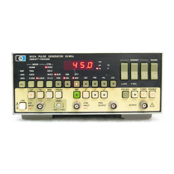
Figure 4-1. HP 81 12A Front Panel Switching On The HP 81 12A performs a "self test" when the power is switched the front panel LEDs should light momentarily. If a fault is detected, the word "ERROR" is illuminated and an error code is displayed on the front panel digital display. - Page 47 Fail Output Amp +ve Offset test Fail Output Amp -ve Offset test Fail Overall tests E41/42 The output amplifier is faulty. Fail Burst Counter tests Refer to Chapter 10.1 Troubleshooting for more information on the error codes and their causes. When the self-test is completed successfully, the instrument automatically assumes the operating state which was active when it was last switched off, excep' t that the output is disabled to...
-
Page 48: Normal
Standard Parameter The Standard Parameter Set exists for two reasons: • If the instrument RAM becomes corrupted due to battery failure, the Standard Parameter Set will be selected when the instrument is switched on to give an error free display. •... -
Page 49: Trigger
Selecting Trigger Mode 8112A PULSE GENERATOR SOMHz HEWLETT -PACKARD ,-- MODE � NORM TRIG 0 GATE D O E .Bi.I Figure 4-2. Trigger Mode Controls Mode Selection The currently active mode is shown by LED indicator. The trigger mode can be cycled through available options by pressing the key below the mode indicators. -
Page 51: Control Mode Controls
Control Input An analog signal can be applied to the control input to modulate or control the HP 8 1 1 2A output signal. This external input may be any waveform in the range ±20 V. However, the overall range within which the instrument actually responds to a control signal, is 1 .0 V... -
Page 52: Mode Selection . ( )
Mode Selection Depending on the control mode selected, the output signal may be either Period, Delay, Width, or High Level controlled, by an external voltage applied to the CTRL INPUT. The control mode can be cycled through available options by pressing the key below the mode indicators and the currently active mode is shown by an LED indicator. -
Page 53: High Level Control Capabilities
4-6. becomes non-operational in this Control mode, and the button LED will blink. See Figure H I L M LOL set (+7. 95\/) - Maximum The d otted line shows the H I LC range Figure 4-6. High Level Control Capabilities Operating 4-9... -
Page 55: Lee And Tre Ranges
Transition Ranges There are seven overlapping ranges for linear and gauss transitions, and it is important to note the following: • Within any range, the maximum ratio of the leading edge transition time to the trailing edge transition time is 1 :20 and vice versa. -
Page 56: Ranging Examples
50ns 99ns 500ns 999ns Range Non-active S lope Active S lc:ipe / / / / / / / / / / JI' / / / / / / / / / / / / / / / / / / / / / / / / ,,,,,,, Range 5 Figure 4·9. -
Page 57: Parameter Controls
Parameters Setting 8112A PULSE GENERATOR 50MHz ,- VERNIER ---- -- RANGE HEWLETT-PACKARD H H H H ,-EXCESSIVE-, o Bi.I o DBL o DTY O PER O DEL O WID o LEE 0 HIL O LOL " RCL uSTO STO/RCL Figure 4· 1... -
Page 58: Width/Duty Key
High and Low level CillD ( LOL ) set. Keys The selected HI1 value is inoperative in the HI1C mode. Note This key causes the HP 81 12A to assume a factory programmed Set Key parameter set as follows: NORM Active Active... - Page 59 The HP 81 12A has the capability to store nine complete sets of mode Store and Recall Key and parameter information in it's memory. To store settings, press (STO/RCL). The digital display now reads unX, where X is the file identity number ( 1 to 9). The right hand vernier key is used to alter the value of X, to determine which fi l e the parameter set will be stored as.
- Page 60 Selecting Output Mode 8112A PULSE GENERATOR 50MHz HElfl.ETT · PACICARD JllJT COll PL DJMll L& G G G � 0 Figure 4· 1 1. Output controls Pressing the (LIMIT ) key sets the current high and low output levels Limited Output...
- Page 61 & Do not apply an external voltage greater than ±5 V, or electrostatic Caution discharge to the output connector. Operating 4-1 7...
-
Page 62: Rear Panel
Refer to Figure 3-3 for a definition of the HP-IB connector pins. HP-IB Connector Refer to "Setting the HP-IB Address" in Chapter 6 if you want to know how to set the instrument's HP-IB address. Not used with HP 81 12A. -
Page 63: Typical Output In Normal Mode
Operating Examples Introduction To obtain an output from the HP 81 12A it is only necessary to set the mode, period and transition type. Then press the green (SET ) key. A stable error free pulse train is generated and you can then alter parameter values, and external input and control modes to derive your desired output. -
Page 66: Typical Signals In External Width Mode
6. If a Control Function is required, select the required mode by repeatedly pressing the control mode key until the required mode is lit. Apply the Control signal to the CTRL INPUT connector. Refer to Chapter 4 for more permissible combinations of Operating Operating and Control modes. -
Page 67: Typical Signals In External Burst Mode
You may wish to set up Output Limits as described in Chapter 4 Note Operating to protect the device under test. 7. Press the (DISABLE) key to turn off output disable mode and enable the output (LED extinguished). External Burst Mode I NPUT ( 50"... -
Page 68: Capacitance Circuit
50 o h m 5 0 o h m l oa d l o a d O s ci l l o s co pe H P 8112A G rou nd ___. ._ 5-6. Figure Capacitance circuit Linear transition mode lndependantly variable leading and trailing edges between 6.5 ns and... -
Page 69: Digital Applications
• Simulation of bandpass filtered signals such as data transmission over telephone lines • Generation of haversines Digital Applications Fixed transition mode Can be used for stimulation of fast logic components and circuits as follows: • Clock generation • Producing known good data inputs for logic sub assemblies and modules •... -
Page 72: Trigger Level
Local Lockout The (LcL) key can be disabled by sending an HP-IB Local Lockout command from the system controller (use the LOCAL LOCKOUT statement in BASIC 5 .0/5 . 1 ) . -
Page 73: Terminators
HP9000 Series 200/300 controller. When connected to other controllers, the HP 81 12A may accept J,F as terminator. The HP 81 12A itself, terminates a data message sent to the computer with: CR/LF followed by a SPACE character The EOI line is not polled by the HP 81 12A. - Page 74 Example: To set the Period to 2.2 ms, the ASCII mnemonic PER followed by the new value 2.2 and the unit MS must be sent to the HP 81 12A. HP Basic Statement for this is: OUTPUT 712 ; "PER 2 . 2 MS"...
- Page 75 The HP 8 1 12A can be programmed into an error condition in just the same way as when using the front panel. For example, attempting to program a larger than HIL: OUTPUT 7 1 2 ; "HIL 1 V , LOL 2 V "...
- Page 76 Selecting Trigger Modes Standard Trigger Modes Mnemonic Action Select NORM Select TRIG Select GATE Select E.WID Select E.BUR Trigger Control Action Mnemonic Select trigger off Select positive trigger slope Select negative trigger slope Select both GATE OUT PUT 7 1 2 ; 11 M3 , T1 11 Example Select mode with a positive trigger...
- Page 77 Selecting Output Waveform Mode Action Mnemonic Select fixed Select linear Select gaussian Select mode off Select mode on OUTPUT 7 1 2 ; "W2 , SM1 11 Example Select linear output waveform transitions S etting Paraf,ll e ters A parameter programming mnemonic is the sa.me as its front panel Note description, DEL delay for example.
- Page 78 Level parameters Action Mnemonic Value Delimiter Set high level volts Set low level volts OUTPUT 7 1 2 ; 1 1 HIL 2 V . LOL - 1 . 2S V" Example Set high level to plus 2 V, low level to minus 1 . 25 V Burst Parameter Action Mnemonic Value Delimiter...
- Page 79 Range Change Action Next higher range Next lower range OUTPUT 7 1 2 ; "RU" Change vernier range upwards Example Stored Parameters Action Mnemonic Value Delimiter 9 Set ident Store parameter set l . . Recall parameter set = Standard l .
-
Page 81: Output Controls
Programming Examples CST command. Also refer to the example program INTERROG. When the HP 8 1 12A replies with a string containing all current settings. The data is always in the same order: M 1 , CTO , T1 , W1 , SMO , LO , CO , D 1 , BUR 00 1 # , PER 1 . 00 MS , DBI. 200 US , DEL 65 . 0 NS , DTY 50 Y. - Page 82 Answer This is the time taken by the HP 8 1 1 2Ato transmit a message when error reporting or learn mode. Time is 1 ms per character, status byte <...
-
Page 83: Status Reporting
40% more efficient . The Buffer Not Empty fl a g in the HP 81 12A status byte is set during this time. The system controller can therefore monitor this flag to detect when a programming message has been implemented. - Page 84 The conditions which cause them and the description (Bit 0) used by the HP 8 1 12A when replying to an IERR command are listed below. The limit error bit is not latched, therefore a transient error is only recorded by generating an SRQ .
- Page 87 (Bit Buffer not Empty This bit is set when there is data in the HP 8 1 12A input buffer. You can monitor this bit to determine if the instrument has finished (Bit interpreting a long programming message.
- Page 88 My talk address selectable An HP-IB D CL command causes the HP 8 1 12A to load its standard parameter set. The instrument remains in its current mode (local or remote). An HP-IB SDC command causes the HP 8 1 12A to load its standard parameter set and enter remote mode.
- Page 89 The hardware settling time must also be considered. (See Chapter 2 for more details). Specifications When a command is sent to the HP 8 1 12A, the device places all received characters into a buffer. Interpretation of the command( s) starts as soon as a valid terminator is received.
- Page 90 Transfer jumper A3W3 at the center of the microprocessor board A3 from the factory setting to position The HP 81 12A (with old and new firmware) does not pull the EOI line. The device terminates all messages with CR/LF and a space character.
-
Page 91: Interrogate Timing
NO MESSAGE instead of the response. Should your computer be too fast for the HP 8 1 1 2A, it will be necessary to force the computer to wait a few hundred milli-seconds before reading the response after an interrogate command. -
Page 93: Introduction
Demonstrates the usage of all types of interrogate commands offered by the HP 81 12A Note In the examples it is not strictly necessary to put the HP 8 1 12A into remote mode using the REMOTE 712 command because: •... -
Page 94: Testing Communication
E N D Programming applications should include an initial check that the HP 8 1 12A is communicating correctly. A suitable quick check is to set a parameter to a particular value and then read it back, as illustrated by the flow chart and program example given here. - Page 95 ! Device addr e s s of the HP 8 1 1 2A CLEAR Adr ! Init ial ize Interf ac e , s et HP 8 1 12A t o CLEAR SCREEN ! Standard s ett ing , an d clear s cr e en...
- Page 97 ! " Execute Self Test" command ( RMT and ADS LED ' s on) WAIT 1000 ! Time for HP 8 1 1 2A int ernal pro c e s s ing A=SPOLL ( Adr) ! Read and clear Status Byt e...
-
Page 98: Using The Buffer Not Empty Flag
Read 8112A's status byte CONTINUE The Buffer Not Empty flag indicates that the HP 8 1 12A is currently interpreting a programming message. You can use the flag to make the system controller wait until a message has been implemented before proceeding. - Page 99 Adr= 7 1 2 ! Addr e s s of the HP 8 1 12A CLEAR Adr ! Initialize int erfac e , s et HP 8 1 1 2A to ! st andard s ett ing and remote mode CLEAR SCREEN...
-
Page 100: Common Task Examples
HP 8 1 12A parameters periodically. In this example every 2 second Delay will be incremented by 1 ms while Width is decremented by 2 The interface is initialized and the HP 8 1 12A is set to the standard Comments... - Page 101 PRINT "Every two s econds delay i s increment ed by 1 ms and w idth is decrement ed" PRINT "by 2 ms . . . " PRINT 2 1 0 ! D e l ay and W idth loop FOR I=O TO 1 0 New_del=9+I * 1 New_w id=22 - I * 2...
-
Page 102: Program Spoll_2
The main purpose of this program is to demonstrate how to service Purpose an SRQ directly in the program. It also demonstrates how to: initialize the interface of the HP 8 1 12A and set it to the standard setting clear the status byte... - Page 103 SPOLL would be conducted whilst "XXX" is being parsed. At this moment there is neither a syntax error or SRQ active. The resultant SPOLL would be 1 28, indicating that the HP 8 1 12A command buffer is not empty. (See Chapter 6 Error, fault and status reporting.
-
Page 104: Intr_2
I NTR_2 This program demonstrates how to use interrupts to service SRQs. Purpose Comments Setup section (llnes 1 10 - 1 20): The interrupt service subroutine Service_srq is set up. SRQs from interface 7 are enabled to cause an interrupt. Main section A SPOLL is conducted to show the value of the STB before the syntax error. -
Page 105: Error_Demo
SUB Service_srq PRINT " - - - - - - - - - - - - - - - - - -- - - - - - -- - - - - - - - - - - - - - - - - - - - - " 3 1 0 PRINT 11 SRQ from HP8 1 12A - - >... - Page 106 ! Name of this program : ERROR_DEMO ! - - - - - - - - - - - - - - - - - -- - - - - - - - - - - - - - - - - - - - - - - - - - - - - - - - - - - - - - - - - - - - - - - " This program demonstrates hov to determine which error bit ( s ) are set in the HP8 1 12A ' s Status Byte .
- Page 107 5 1 0 PRINT WAIT 2 PRINT " The following bits are set in the Status Byt e : " PRINT WAIT 2 No bit i s s et . " IF A=O THEN PRINT --> IF B I T ( A , 7) THEN PRINT Bit 7 Buffer Not Empty "...
-
Page 108: Learn String (Double Mode Active)
LR N_DEMO This program demonstrates the Learn String's usage: P urpose • Reading the current Learn String with CST • Sending the Learn String back to the HP81 12A • Time taken for transferring the Learn String is printed • Recalling a setting from a location is shown (RCLO) There is no direct command in the Learn String which indicates Comments... - Page 109 A=SPOLL ( 7 1 2 ) clear St atus Byte 1 50 DIM A$ [ 1 53] The L e arn String cons ists of 153 ASC I I charact ers . 1 60 PRINT " Re c all ing s ett ing from locat ion 0 (Standard S ett ing) .
-
Page 110: Interrog
INTERROG The current sett ing of the HP 8 1 12A is : Y, , WID 100 US , LEE 10 . 0 NS , TRE 10 . 0 NS , HIL + 1 . 00 V , LOL +0 . 00 V , M1 , CTO , T 1 , W2 , SMO , LO , CO , D 1 , BUR 000 1 # , PER 1 . - Page 111 CLEAR SCREEN init i al ize int erface and HP8 1 1 2A CLEAR 7 1 2 clear status byte 1 0 0 A=SPOLL ( 7 1 2 ) 1 10 1 20 L e arn String interrogate funct ion CST ( Current S ett ing) DIM S ett ing$ [ 1 53] OUTPUT 7 1 2 ;...
- Page 112 58 0 59 0 OUTPUT 7 12 ; 11 IBUR 11 ENTER 7 12 ; Burst $ 6 1 0 PRINT "Respons e after !BUR command : " ; Burst$ PRINT PRINT " End of the program I NTERROG . 11 LOCAL 7 1 2 rttp Programming Exa...
-
Page 114: Test Equipment
P, A 50 MHz, Start/Stop, HP5345A Counter HP 5335A with OPT 040 TI, A to B P, A, T DC 0.01 V-50 V, .0043 acc. HP 3478A Digital Voltmeter HP 3458A P,A,T Pulse amplitude facility HP 3456 HP3324A #002 P, A 20 MHz, THD �... -
Page 116: Specifi C Ations
Test Record, specified limits are given here and on the Test Record. Collll t er reading HP 81 12A setting Low Limit High Limit 17.0 23.0 µs µs µs 10.5 10.5 950 ms 902.5 997.5 Delay Performance Test Specifications... -
Page 117: Delay Performance Test
---+ Gate Mode 4. Set the HP 8 1 12A Delay and Period to the following values and read the actual output from the counter. Record your results on a copy of the Test Record, specified limits are given here and on the Test Record. -
Page 118: Double Pulse Performance Test
Digitizing Oscilloscope with Accessory (HP 54121 T) Equipment • Counter (HP 5335A) • Cable, 50 BNC to BNC, coaxial, 2 each (HP 8120- 1839). • 20 dB attenuators • feedthrough termination ( Required if counter input impedance f 50 Test Setup 1... -
Page 119: Double Pulse Performance Test
65 ns 1 .00 - 1 .00 3. Connect the HP 8 1 12 TRIG OUTPUT via a BNC to S MA adaptor and a 20 dB attenuator, to the TRIG Input of the HP 54121A. 4. Connect the HP 8 1 12 OUTPUT via a BNC to SMA adaptor and a 20 dB attenuator, to Input 4 of the oscilloscope. -
Page 120: Pulse Width Performance Test
17.0 lOOµs µs µs 19.0 µs 2 1 .0 µs 8. Connect the HP 8 1 12A to the counter as shown in Test Setup 2 Set the counter as follows: Trigger level Preset Mode PER A Impedance Gate Mode... -
Page 121: Pulse Width Performance Test
1 .00 v - 1 .00 v 2 . Connect the HP 8 1 12A and oscilloscope as shown in Figure 8-5 . 3 . Verify that for the following HP81 12A WID settings the scope display indicates that the HP 8 1 12A output is within the specified limits. -
Page 122: Constant Duty Cycle Performance Test
7 . 5 1 2 . 5 200µs 40 µs 38.0 µs 42 .0 µs 5. Connect the HP 8 1 12A and counter as shown in Figure 8-6. 6. Set the counter as follows: Trigger level - Preset Mode Time A �... -
Page 123: Duty Cycle Performance Test
- 1 .00 3. Set the counter to DTY CY A. Set the HP 81 12A DTY to the following values and read the actual output from the counter. Record your results on a copy of the Test Record, specified limits are given here and on the Test Record. - Page 125 4.76 v 5.24 v 8.0 v 7.64 v 8.36 v 6. Set up the HP 8 1 12A as follows: 65 ns 0.0 v -0.10 v 7. For each value of LOL in table, verify that the DVM reading is within the specified limits.
-
Page 127: Fast Transitions
Linear +5.00 v 0.00 v • For the HP 81 12A to the settings in the table below, measure the displayed leading edges and trailing edges • Verify that the transition times do not exceed the specifi e d limits. -
Page 128: Pulse Performance Test
0.00 v 3. Adjust the oscilloscope so that one pulse fills the display. 4. Examine the HP 81 12A output on the scope display in order to verify that the pulse characteristics do not exceed the specified limits as identified in Figure 8-1 1 . -
Page 129: Specifi C Ations
Linear 6.5 ns 6.5 ns Examine the HP 8 1 12A output on the scope display in order to verify that the pulse characteristics do not exceed the specified limits as identified in Figure 8- 1 1. 8 . Record your results on a copy of the Test Record, specified limits are given here and on the Test Record. -
Page 130: External Width
Overshoot Amplitude Pre-shoo t Figure 8-1 1 . Pulse Performance Characteristics Trigger ,Gate,E. Width and E.Burst Verification Test Characteristics Trigger Minimum 500 mV p-p) amplitude 10 ns Minimum pulse width Each active input generates one output pulse. Gate • External signal enables Period Generator. •... -
Page 131: Control Modes
Control Mode Transition Fixed 2.0 µs 65 ns 1 .0 µs 1.00 v 0.00 v 3. Set up the external pulse generator (HP 8 1 1 6A) as follows: Frequency 50 kHz Width 5.0 µs Amplitude 2.0 V Offset 0.00 V 4. - Page 132 (I N PUT 2) TRIG OUTPUT (I N PUT 6. Set the HP 81 1 2A to GATE trigger mode, PER 900 ns and DTY = 50%. Verify that each gate leading edge releases a train of output pulses and that each cycle is complete. As shown here.
-
Page 133: Output Mode Verification Test
12. Using the oscilloscope, adjust the HP 8 1 1 2A trigger level to allow triggering from the negative going edge of the external input signal. 13. Set the oscilloscope sweep speed to 2 µsf division. 14. Verify that each external trigger pulse generates a burst of 50 output pulses as shown here. -
Page 134: Output Mode Verification Test
• 50f! Feedthrough Termination required if counter input impedance 50f! 1 . Connect the equipment as shown in the setup 1 figure Procedure 2. Set up the HP 81 12A as follows: Trigger Mode NORM Control Mode Transition Fixed 1 .0 µs... -
Page 135: Period Control Verification Test
Slope A preset Trigger level 13. Press the (MAN ) key on the HP 8 1 1 2A to simulate an external trigger and verify that the counter counts 4 72 pulses. 14. Press the (1 key and confirm that the counter reading increments to 4 73. -
Page 136: Delay Control Verification Test
1 volt and 10 volts, and verify that the counter display indicates a range of periodic times which agree with the specified limits for each of the HP 8 1 1 2A settings below. HP 81 12A Counter... -
Page 137: Correct Delay Control
50 ns 2.00 v 0.00 v 3. Vary the power supply or HP 3324A between approx 1 volt and 10 volts and verify that oscilloscope display indicates delay time of between 75 ns and 1 70 ns as shown below. -
Page 138: Width Control Verification Test
7. Vary the power supply between approx 1 volt and 10 volts and verify that for the following HP 8 1 1 2A settings, the range of times displayed agrees with those specified. 81 12A Counter setting reading High 100 ns... -
Page 139: High-Level Control
3. Set the counter to PULSE A 4. Vary the power supply or HP 3324A between approx 1 volt and 10 volts and verify that for the following HP 8 1 1 2A settings, the pulse width range agrees with those specified. -
Page 140: High-Level Control Verification Test
Trigger Mode NORM Control Mode HILC Transition Fixed 200 µs 65 ns -2.00 3. Set up the HP 81 1 6A Pulse/Function Generator as follows: Output Sinewave Frequency 50 Hz Amplitude 16.0 V Offset 0.00 V 4. Verify that the High-level output can be varied between +8 V and - 8 V while the - 2 V level remains unchanged as shown below. -
Page 141: Correct Delay Control
6. Set up the HP 81 16A Pulse/Function Generator as follows: Output Squarewave Frequency 1 kHz Amplitude 2.0 V Offset 0.00 V 7. Verify that the scope display indicates a settling time of less than 200 µs as shown below. - Page 143 5. Verify that the settings are the same before, except for the following: PER 10 . 0 MS DTY 10 Y, HIL 1 . 50 V 6 . Using the oscilloscope connrm that th� HP 81 12A output has the following form: Pulses Square Period 10 ms...
- Page 144 Testing Performance 8-32...
-
Page 145: Performance Test Record
PERFORMANCE TEST RECORD: Hewlett-Packard 8 1 1 2A 50 M Hz Pulse Generator Serial No: --------------------------- Report No: -------------------------- Date: ------------- Test Facility : Test Conditions : Installed Options : Ambient Temperature : Relative Humidity : Line Frequency : Special Notes : Testing Performance 8-33 PERFORMANCE TEST RECORD Page 1 of... - Page 146 PERFORMANCE TEST RECORD: Hewlett-Packard 8 1 1 2A 50 MHz Pulse Generator Serial No: --------------------------- Report No: -------------------------- Date: _ _ _ _ _ _ _ _ _ _ _ _ _ Test Equipment Use(j : Cal.Due Date Description Model No. Serial No.
- Page 147 PERFORMANCE TEST RECORD: Hewlett-Packard 8 1 1 2A 50 MHz Pulse Generator Serial No: Report No: -------------------------- Date: - - - - - - - - - - - - - - - - - - - - - - - - - - - _ _ _ _ _ _ _ _ _ _ _ _ _ Period Period Minimum MEASURED Maximum Uncertainty...
- Page 148 PERFORMANCE TEST RECORD: Hewlett-Packard 8 1 1 2A 50 MHz Pulse Generator Serial No: --------------------------- Report No: -------------------------- Date: ------------- Pulse Width Pulse Period Width Minimum MEASURED Maximum Uncertainty 100 ns 10 ns 7.5 ns 12.5 ns Settings Period Width Minimum MEASURED Maximum Uncertainty 200µs 40 µs 38.0 µs...
- Page 149 PERFORMANCE TEST RECORD: Hewlett-Packard 8 1 1 2A 50 MHz Pulse Generator Serial No: Report No: -------------------------- Date: ------------- - - - - - - - - - - - - - - - - - - - - - - - - - - - -0.
- Page 150 PERFORMANCE TEST RECORD: Hewlett-Packard 8 1 1 2A 50 MHz Pulse Generator Serial No: --------------------------- Report No: -------------------------- Date: ------------- Pulse Performance Fixed Transition MEASURED Uncertainty Characteristic Specification Preshoot �±10% of amplitude ±10 mV Overshoot /Ringing �±10% of amplitude ± 1 0 mV Settling time �...
-
Page 151: Output Modes
VERIFICATION TEST RECORD: Hewlett-Packard 8 1 1 2A 50 MHz Pulse Generator Serial No: --------------------------- Report No: -------------------------- Date: _ _ _ _ _ _ _ _ _ _ _ _ _ Trigger, Gate, Extern�I Wtdth and Burst Modes Trigger Positive trigger initiates one complete output cycle: YES/NO Gate... -
Page 152: Store And Recall
WID Minimum and Maximum achieved YES/NO µs YES/NO 100 ms YES/NO -2 V level remains unchanged: YES /NO High-Level Control YES/NO Settling time correct: Store and Recall YES/NO HP-I B programming HP-IB functioning: YES/NO 8-40 Testing Performance VERIFICATION TEST RECORD Page 2 of 2... -
Page 153: Procedure
Shaper and Offset Adjustment • Slope Note Always allow the HP 81 12A to warm up for at least 1 hour before starting any adjustment procedures . The Power Supply and Preliminary adjustment procedure must be carried out after any repairs. - Page 154 Always carry out an adjustment procedure completely and in the order in which it is presented. If the HP 81 12A is very badly out of adjustment , turn A 1 R4 1 3 fully clockwise and all other adjustment potentiometers to their mid position.
-
Page 155: Complement
Table 9-1. Adjustment Procedures - Changeable Components (continued) Description Reference Range Procedure Range capacitor Delay 22 pF A1C220 Bias adjustment A1R225 215n Both infl u ence linearity of A2VR4 open or 4.3 V Delay Generator A2R64 open or 51 .1 kn used to get A2R14 (DEL 1 ms Adj . -
Page 156: Access To The Hp 8 1 1 2A For Adjustments
HP 81 12A instrument and prepare for servicing> M i c r o p rocessor B oar d Control Board � Figure 9-1. Access to the HP 8 1 1 2A for Adjustments Power Supplies Digital Voltmeter (HP 3456A) Equipment 1 . -
Page 157: Disable
DISABLE Off ( Enable) LIMIT 2. Connect the HP 8 1 12A main output to the oscilloscope input 4 via 40 dB (2 20 dB) attenuation. 3. Connect TRIGGER OUT of the HP 81 12A to the TRIG IN of the oscilloscope, via a 20 dB Attenuator. -
Page 158: Trigger Output
9. Set the HP 81 12A Transition to FIXED. 10. Set the HP 81 12A output to COMPL off. 1 1 . Connect the HP 81 12A trigger output to the oscilloscope trigger input via 20 dB attenuation. 12. On the oscilloscope press (Autoscale) and set for 2 V /div vertically and 200 µs/div. -
Page 159: Overshoot Transition Time Adjustment
Off (=Enable) LIMIT 2. Connect the HP 8 1 12A main output to the oscilloscope input 4, via two 20 dB attenuators ( 40 dB ) . 3. Connect the H P 8 1 12A trigger output t o the oscilloscope trigger input via 20 dB attenuation. - Page 160 13. Repeat steps 7 to 1 1 using 90 - 1 103 / - 10 - 103 and adjust A1C410 for overshoot < 103 in both normal and complement modes. 14. Set the HP 8 1 1 2A as follows: - 2.0 LIMIT 15.
- Page 161 18. Take full screen display on the scope. Check that the transition times <4.8 ns in both normal and complement modes. 19. Set the HP 8 1 12A to Linear transition. 20. Measure the transition times are <6.2 ns. Note Transition times can be increased by increasing the overshoot .
-
Page 162: Timing
DISABLE LIMIT 2. Set the counter for Period measurement . 3. Connect HP 8 1 1 2A output via a 50!1 feedthrough to the counter. 4. The typical period accuracy of the period decades is as shown in Figure 9-4. - Page 163 Trigger (both chan) = 50 20. Connect HP 8 1 1 2A Trigger Output to channel A of the counter. 2 1 . Connect HP 8 1 12A Output to channel B of the counter. 22. Set trigger levels to trigger at about 503 of amplitudes.
- Page 164 3 1 . Connect HP 8 1 12A Trigger Output via a 20 dB attenuator, to Ext. trigger of the HP 54121A. 32. Connect HP 8 1 1 2A Output via a 20 dB attenuator to input 4 of the HP 541 21A.
-
Page 165: Equipment
12. Connect HP 8 1 12A Trigger Output via a 20 dB attenuator, to trigger input of the HP 54121A. 13. Connect HP 8 1 1 2A Output via a 20 dB attenuator to input 4 of the HP 54121A. - Page 166 16. Adjust the low range end with A2R59 for 101 ns ±0.2 ns. 1 7. Repeat previous six steps and re-adjust if necessary. 18. Alter HP 8 1 1 2A WID to 50 ns. 19. Check that Min. width is 50 ns ± 2ns.
-
Page 169: Low Pass Filter
+8.00 +7.90 34. Set up the DVM to read DC voltages up to 10 V. 35. Connect the HP 8 1 12A main output via an exact 50 0.13 feedthrough terminator to the DVM, and enable the DVM built-in fi l ter. If the DVM does not have a built in fi l ter, use a low-pass fi l ter as shown in Figure 9-6. - Page 170 +8.00 COMPL DISABLE LIMIT 4 1 . Connect the HP 8 1 1 2A output via an exact 50 0 . 1 3 feedthrough, t o the oscilloscope ( HP 54503A). 42. Adjust A2R50 for 0 V amplitude (no signal).
-
Page 171: Test Setup
Slope • Equipment Oscilloscopes (HP 54121 T /HP 54503A) • 20 dB attenuators (3 Procedure 1 . Set up the HP 8 1 12A as follows: Trigger Mode NORM Control Mode 5 ms 65 ns Transition Linear 100 µs 500 µs +4.00... - Page 172 7. Connect the HP 8 1 1 2A Trigger Output to the oscilloscope Trigger Input. 8. Connect the HP 8 1 12A output to input 4 of the oscilloscope. 9. Set the oscilloscope to display one pulse using the mode.
- Page 173 500 ns 1 00 ns 1 00 ns 32. Connect the HP 8 1 12A to the HP 54121A oscilloscope using two 20 dB attenuators. 33. Set the oscilloscope to display one pulse and set it to measure Rise/Fall time.
- Page 174 P/O RI ED RY ADJUSTMENT POI NTS HP 8 I 12A BOARD A l -23V • ""' -c:BLJ- +SV -cBLJ- --'5.Z"' � -15V -cr r: ::J- -l3V Figure 9-8. Adjustment Points on the Main Board A 1 9-22 Adjustment Procedures...
- Page 175 P / O R2 BO R Y ADJUSTMENT PO I NT S H P 8 1 1 2 R BOARD R2 TRE/LEE TRE/LEE 1 0ms TRE/LEE 7 . 95V OFFSET 99. 9ms " [;j � W I D ��D 0V WW HILC PERIOD PERIOD...
-
Page 177: Safety Check
Capacitors inside the instrument may still be charged after the instrument h�s been disconnected from its external power supply • • The HP 81 1 2A contains static-sensitive devices. ATTENT I ON Ensure that "static-safe " precautions are taken to Static Sensitive prevent electro-static discharge when the instrument covers are removed. - Page 178 5. Check that the case is isolated from the power-cord power-pins & VDE. If a problem exists, it must be in accordance with IEC investigated and fixed before proceeding. 6. Check that the correct line fuse is fitted. 7. Check that all safety covers are fitted. 8.
-
Page 179: General
Component layouts for each board assembly are also provided. The five board assemblies contained in the HP 8 1 1 2A are listed in Table 1 0- 1 which lists the servicing chapters applicable to each board. - Page 180 Table 10-1. & HP 8 1 1 2A Board Assemblies Servicing Chapters Chapter(s) Reference Main Board 10.2, 10.3, 10.4 Control Board 10.5, 10.6 Microprocessor Board 10.7 Keyboard 10.7 Display Board 10.7 10-4 Introduction to Servicing...
- Page 181 1 0. 1 Instru ment Overview and Troubleshooting Guide The block diagram in Figure 10.1-1 shows the HP 81 12A at a Theory of Operation functional level. DISPLAY BO KEY BOARD BURST BURST OFFSET CLOCK COUNTER BURST OPT I ON...
- Page 182 T li'£ IN Rfff' FREQ �T ON ERROR OUT EXT C l a..R REN T NOTE T I M ING IC Figure 10.1-2. Custom ICs used in the HP 8 1 1 �A 1 0. 1 -2 Instrument Overview and Troubleshooting Guide...
- Page 184 HP - I B POWER ON JAMMED LAMP TESTS TESTS 1_ n I TEST T I M I NG TESTS DELAY W I DTH & TRE STOP 1 O. 1 -4 Instrument Overview and Troubleshooting Guide...
- Page 185 Key Jammed Possible faulty A3 Processor Board (ROM reset circuit ) or power supply fault (restart signal) A front panel key is stuck. The instrument cannot be used until it is freed. RAM Test E0 1 The microprocessor is unable to load a test pattern into the RAMs U lO/U l l and verify it .
- Page 186 F I XED MOD E O K ? E :J :J O K ? L I NEAR MODE T m� RC O K ? 10.1-6 Instrument Overview and Troubleshooting Guide...
- Page 187 Output Amplifier Tests E2 1 Offset generator is unable to produce positive offset . Possible failure in Output amplifier or offset control circuit U l 7 to Ul9, U20 to U22, or U27. See Chapter 10.4. Offset generator is unable to produce negative offset . Possible failures as E21 .
- Page 189 Test Amplitude range 1 not possibl�. Possible faults as in E41 . HP 8 1 1 2A set to produce a burst of 10 pulses of period 250 µs. Burst Tests E5 1 Burst counter supplies less than 10 pulses. Possible fault in Burst fl i p-flop U201 or Burst control circuit U102 to U 1 12 .
- Page 191 1 0 . 2 Servicing the Power Supply Theory of Operation The HP 8 1 1 2A power supply unit occupies part of the main Introduction board Al and consists of the following four parts, as shown in Figure 1 0.2- 1 : •...
- Page 192 Table 1 0.2-1 . Power supply rectifiers Rectifier Output ±5 V DC ±23 V DC ±15 The raw voltage outputs are all smoothed by capacitors, as shown in Figure 10.2-3. The following supplies are then fed to voltage regulators, with potentiometers to adjust the final voltage level: Table 1 0.2-2.
- Page 193 (5.1 V) than its non-inverting input (5 V). When the HP 8 1 1 2A is switched off, the 5 . 1 V supply breaks down faster than the 5 V reference because it is loaded by the microprocessor board.
- Page 194 10.2-4 Servicing the Power Supply...
- Page 195 P / O M A I N B O A R D SERV I CE J I C 2 > LI NE VOLT AGE 8EL£CTIIR , - - PIO A l MA I N 1• 121 1 • • 22flV 24 8¥...
- Page 198 SERV I CE +2 3Y 1112 Al /11 7 l. 4 7 u 4 ,._ i•·lu +ISY J 4 Cl2> TO A2/J4 i s . CONTROL BO i · [ill 1.115 i ZZlkJ CURRENT SENSOR REF' AC.I .J 1 . zv CIRCUIT J 4 Cl 3 ) REF"ERENCE...
- Page 200 . -- i • POW E � : • ,,..-nr' DOWN I 5.1 • �· � > � • • I -- :i.. L-- - J r;- -;i • 14 • • I DE 1C CT • �...
- Page 201 1 0 . 3 Servicing the Timing and Slope Generators Theory of Operation The majority of the timing and slope generation circuit components Introduction are on the main board A l . A small part of the associated circuitry, concerned with burst control, is on the control board A2. Operation of the timing and slope circuits is explained under the following functions: •...
-
Page 202: Control Input
10.5. The low pass filter is needed because of the 20 µs settling time inherant in HILC mode operation. The timing ICs used in the HP 8 1 12A are programmable timers Timing IC which can be used to produce repetition rates, pulse widths and delay times by utilizing a variety of trigger and gate mode inputs. - Page 203 � "' > "' "! � "' l � "' "' "' "' OUTPUT SWITCHING RANGE CONTROL INPUT STORE � rd � I� f- a: RANGE >: "' °' -5 . 2V Figure 1 0.3· 1 . Timing IC block diagram Refer to Figure 1 0.3- 1 and Figure 1 0.3-6.
- Page 204 In TIME mode the ranges are from 1 0 ns to 99.9 ms and 50 ns to 500ns. In RATE mode, ranges are from 1 00 MHz to 1 0 MHz and 20 MHz to 2 MHz. Ranges are selectable as shown in Table 1 0.3-3. Table 1 0.3-3.
- Page 205 Because CUR REF, FRQ IN and TIME IN are virtual earth inputs, the external input currents can be produced by a voltage source and series resistance. The control mode functions (PERC , DELC, WIDC) are produced by feeding the conditioned control input voltage to the TIME IN input of the relevant timing IC.
- Page 206 The IC is either free running or triggered by the EXT INPUT, depending on the state of the internal trigger mode latches (data from LD5 to LD7). The inverse output O UT is passed to the trigger amplifier (Chapter 10.7) for subsequent output as TRIG OUT. Normal output OUT, is passed via level shifter Q200 to the delay generator trigger input .
- Page 207 Slope Generation CCNTRCL SIGR..FIXED SLCF'E - s . 2 v TRI G IN FRCl1 WIDT H GENERATOR EECL JUL.r RAt'P a=FACITOR : SQ-IMtTT TRIGCER l2.srnA 14 La.I LEVEL ADJUST OUT BIAS R:3 1 a . +6.2V Figure 1 0.3-3. Slope IC block diagram Refer to Figure 1 0.3-5 and Figure 1 0.3-3.
- Page 208 Current Sources External constant current sources on the control board A2 provide re f re f · and Idown When a rising edge is detected at TRIG IN, Q303 is switched on via the internal buffer to enable one of the internal or external ramp capacitors to charge up linearly by Iup re f (derived from Iup...
- Page 209 P I O M A I N B O A R D ADDRESS DECODER MODE DECODER c 1•1 N.C. 3 . 3p Ulll N.C. FROM A3 J2( 4 ) MI CROP . BO J5/W4 J2(9) JZCI> JZUI> J2(7) JZ U U 7 4Ul273N II J2(13) J2U2l...
- Page 210 SERV I CE RANGE DECODER IX4, Z.ZlK ltll2 74LllZ73N Z. ZlK 0 Ulll.11 11113 -s. zv BURST -s.zv 11111 4. 7 p 1 79 l.lK Tl. lu Tl.lu a.ac ::-l -5. ZV -5. ZV Rlll 11. 1 Ulll/8 CONTROL MODE Ulll/11 ·lliJ SELECTOR...
- Page 211 P I O M A I N B O A R D � M " FROM A2 CONTROL BOARD J4(4 J4C3 PER I OD GENERATOR GENE L.Olll -LD 7 � RATEl U2BB 24.IK ll.IK •· lu 24. IK 81.IK •. lu 18 1 7 1 8 11214 31.llC...
- Page 213 P I O M A I N B O A R D RAMP CURRENT SOURCES RAM P +urv +lllV +lllV I DOWN REF , .. l .121< R382 ,., l . 121< �l. lu 039 1 C313 1139 1 I UP N.C .
- Page 214 SERV ICE MP CURRENT SOURCES •llY +lllV I UP R3l l 13 . 3 REFERENCE R3ll +111V � C321 1 .. R32 1 +l5V 11328 1 . 151< l..,.U l..:F" 21*' U3Ql1 It.OPE TRIG IN R314 R31S 2.21K 88. 1 -S.
- Page 215 Troubleshooting • If an error code is being displayed by the HP 8 1 12A you must press Note a key, for example, to return the microprocessor to normal operation before troubleshooting. • The component layout and locator for the main board Al is at the end of this chapter.
- Page 217 Table 1 0.3-6. Address Decoder Signatures Connector Mnemonic Description Free run Area A3W4 S.A. Sub coded address P50H U l00/1 Sub coded address CH9U Ul00/2 Sub coded address 8759 Ul00/3 Enable address decoder 1P50 U l00/4 Data load signal for U500 PU99 U500/1 1 see chapter 10-4 Error feedback gate signal 9H1P...
- Page 218 UlOl/16 is LOW in normal mode and HIGH during self test . To check operation of the Ext. Input Circuit: Period Generator 1 . Set up the HP 8 1 12A as follows: Mode Trig Trig Slope Trig Level Pot Mid-range 2 .
- Page 219 - 0 . ? V - 1 . 6 V � � 7 0 n s Figure 1 0.3-9. Period Generator ramp signal pin 20 3. Check the trigger output signal at pin 2 1 of U200 against Figure 10.3- 10. 4.
- Page 221 Note Delay Vernier Current can be checked by measuring the voltage across R226. 7. Set HP 8 1 1 2A PER to 20 ms 8. Check the Delay Generator levels against Table 1 0.3-13 Table 10.3-13. Delay Generator Signal Levels DEL Setting Voltage across R226 +0.16 v...
- Page 222 ___, 70ns -0 . 6 V :::: : � - 1 . B V � � 1 00us Figure 1 0.3-14. Width Generator ramp signal 4. Check the signal being sent to the slope generator IC at TP3 against Figure 10.3- 15. -0 .
- Page 223 +0.004 v 9.99 -0.02 v 1 . Set the HP 8 1 1 2A to R CL 0 and press the � key: Slope Generator 2. Check the input signal from the width generator at pin 1 of U301 against Figure 10.3- 16 3.
- Page 224 5. Verify that the voltages at U301 pins 1 1 / 1 5 are at REF voltage (typ. + l .85 V) 6. Verify that the voltage at U301 pin 13 is at TTL LOW level ( typ. +90 mV) Range Decoder 1 .
- Page 225 1 0 . 4 Servicing the Shaper and Outp ut Amplifier Theory of Operation The shaper and output amplifier circuits are located on the main Introduction board Al and are divided into the following parts: • Bus Latch • Shaper IC •...
- Page 226 AP'F'LI TUOC / " SYP+£TRY VERNIER CONTROL ADJUST CONTROL VOL TAG£ SELECT ADJUST N . C . NORWCO.-F'L t£G NPUT N . C . INPUT NORM/COl"PL OF"f"SET ADJUST RfoFl..ITUOC RD.JUST +SV -5 . 2. V SELECT Fff'L I TUIE AO.JUST Figure 1 0.4-1.
- Page 227 The operating principle is lb . illustrated in Figure 10.4-2, and depends on Q lA and Q l B being a matched pair so that Ia In the HP 81 12A Q lA Q400A, Q l B Q400B and Q2 Q402.
- Page 228 ( Q l A A N D 0 1 8 ARE A MATCHED PA I R ) I BE O l B O l A Figure 1 0.4-2. Current Mirror The pre-attenuator circuit is controlled by the microprocessor via Pre-Attenuator latch U500.
- Page 229 R f b R i n S I GNAL 5 0 OHM OFFSET CURRENT CONTROL R i n Ro f f s OFFSET Figure 1 0.4-3. Simplified Output Amplifier circuit The circuit is effectively an inverting amplifier with a voltage gain R fb given by R ·...
- Page 230 In normal mode the TRIG OUT signal is a 503 duty cycle square wave at the same frequency as the main HP 81 12A output . In TRIG and GATE modes, the TRIG OUT signal is a pulse-shaped equivalent of the trigger input.
- Page 231 SERV ICE ";./ 1425 �- CURRENT M I RROR R419 R4211 14. 7 �l.47u 14. 7 llU514 R438 llR42l 147 1HIER l.541< CR41l R4ll CR414 -s.zv N.O. PRE-ATTENUATOR llC414 lip 1111 V -18V � 0413 1 . Sp OVERSHOOT F'IXED R4 3 1 lM CR412 8 .
- Page 232 P / O M A I N B O A R D ® +lSV BIAS R :: R438 4.141< lK +lSV 1111 4 23 1111 4 • l.lK R437 18.ZK VENll ADJ( OFF'SET LIN. R497 N.C. N.C. R418 249 R484 R418 274 l.BZK WAYE...
- Page 233 SERV I CE +S Y RSl57 2X4. 7K 4.71< +Z3V Rl5S7 4.71< 0521 N.C. 'Jl.47u i- Z79u CSZ3 BEAD [ill @ Rl5llZ BZ.15 0519 81.81< 'Jl. 47u 115 ' +l5V LEVEL CHECK [}£]@ 4. 7K ZX 4 .7K Rl5S7 3. 83 74Ul83N 0518 8.481<...
- Page 234 P / O M A I N B O A R D OUTPUT AMPL I F I ER +'DV +'DV ll .I RS24 OFFSET CURRENT +l5V - · COMPENSAT I ON +24V OYDtSH:IOT CS31s YR51l +l5 V CS2I RSl8 L.Sl CSl2 l.
- Page 235 Troubleshooting a key, ( LCL) for example, to return the microprocessor to normal • If an error code is being displayed by the HP 8 1 12A you must press Note operation before troubleshooting. • The component layout and locator for the main board Al is at the end of this chapter.
- Page 236 GRUSS -0 . 0 5 V Figure 10.4-9. Shaper IC Output (LINEAR) 8. Change the HP 81 12A HIL to +0.99 V and transition mode to FIXED . 9. Check the output on TP6 against Figure 10.4- 10 Figure 1 0.4-10. Shaper IC Output (FIXED, HIL +0.99 V)
- Page 237 Linear Gauss Output Mode Norml COMPL Check the amplitude-vernier control-voltage with the HP 8 1 12A Shaper IC HI1 and 101 settings as indicated in Table 10.4-4. The voltage is Amplitude-vernier measured at the board connector side of R422. Control-voltage Table 1 0.4-4.
-
Page 238: Output Amplifier
-7.9 v -8.0 v +7.45 v Output Amplifier • Do not operate the HP 8 1 1 2A without the heatsinks fitted on Caution board Al • If you need to replace one or more of the transistors Q505 - Q513, do not attempt to remove the heatsink and transistor adaptors together, this is likely to damage the transistors. - Page 239 7. If there is distortion, check the output-amplifi e r input signal at TP4. Then do the following: a. Set up the HP 81 12A as follows: +8.0 v -8.0 v b. If the input signal is clean but the leading edge of the output signal is distorted, check Q503 and Q505.
- Page 240 10.4- 1 6 Servicing the Shaper and Output Amplifier...
- Page 241 MOIEL H"B 1 1 2A R l 1 9 +23V -1 SV -5 . 25V NOTE: all TI£ NON. COtf'Ot£NT SIIE OF' C l 4 1 , C4 1 5 , H l nTTED n£ BOFRD Ulli!B, CXlN£CT(lR BOARD LAYOUT C141 nTTED I.NIER IC C4 1 5 FITTED I.NIER nG..R: ll!l.
- Page 242 B D R Y MR I N • • • • • • · · CR 1 + "' "'...
- Page 243 MODEL HP8 1 1 2A GRID REF . GRID GR ID REF . GRI D REF . GRID REF . GR I D REF . GR I D REF . REF . GRID REF . LOC . DES . LOC . LOC.
- Page 245 1 0 . 5 Servicing the Control Board Theory of Operation The main function of the control board A2 is to convert digital Introduction control data into analog control signals used on the main board A l . The main board supplies power to the control board and the microprocesor board A3 supplies the digital control data.
- Page 246 The timing range decoder U2, controlled by RCT from U l , latches Timing Range Decoder data from the data bus which is then used to select the timing ranges required by the period, delay, width and transition time control sources.
- Page 248 The time difference between LRC , enabling U23, and LRC , enabling new data for U20, is the propagation delay through U19. Offset DAC The offset level output from U21 can be attenuated using R42. The offset DAC U20 is a 1 2-bit multiplying device which provides l out l two output currents.
- Page 249 SERV I CE T I M I NG COMP/H I GH BYTE BURST - lYREF' REFERENCE LD1H.01 1. 1u T I MER FROM A3/W4 M I CROP . BD...
- Page 250 P / O C O N T R O L B O A R D ADDRESS DECODER OUTPUT � J4(28) N.C. J4<lll .14(11) J4(9) J4Cll J4(3) J4(2) 74Ul l- J4 ( l ) FROM A l J4( l l ) DAC SUPPLY •...
- Page 253 SERV I CE ® llf"f"SET R32 ADJ 999ue UP CURRENT SOURCE 11111< -s.zv Al /11 7 > 11151< +lSV • 2. 2K � 8. ZSK l . 47K ® TO A 1 /W 7 l . 27K 7. 111< 1 ... MA I N BOARD ®...
- Page 254 P / O C O N T R O L B O A R D ® orrsc LDlll - LD7 UP CURRENT SOURCE +5V REO +15V 119< �c � @ All" "34 Z. 2K llA1N AD7522 ® 1 . 271< 7 .
- Page 255 Troubleshooting a key, ( LCL ) for example, t o return the microprocessor to normal • If an error code is being displayed by the HP 81 12A you must press Note operation before troubleshooting. • The component layout and locator for the standard control board A2 is at the end of the chapter.
- Page 256 Table 1 0.5· 1 . A2 Address Decoder Signatures Area Free run Description Mnemonic S.A. HHF2 U12,U 13/25 High Byte Slope 63A2 U 13/24 Low Byte Slope (TRE) LBS2 FAFP U 12/24 Low Byte Slope (LEE) LBSl U2/ 1 1 Range Compensation 9CPH U4,U5,U6/25...
- Page 257 +l.95 v 9.99 ms +0.98 v l . Set the HP 8 1 1 2A to RCL 0, PER 15 ms Delay Control 2. Check the Delay DAC output according to the following table: Table 1 0.5-4. Typical Delay Control DAC Output...
- Page 258 1 . Set the HP 8 1 1 2A to RCL 0, PER 15 ms Width Control 2. Check the Width DAC output according to the following table: Table 10.5-5. Typical Width Control DAC Output HP 8112A WID Voltage at TP2 +9.8 v...
- Page 259 HIL + l .99 V HIL -7.9 V HILC Mode Area U25/10 U25/9 1 . Set the HP 81 12A as follows: Offset Control Output Enabled 2. Check the offset DAC's output-voltage against the following table. necessary you can also check that the DAC is receiving the correct data from the offset latches.
- Page 260 81 12A Timer Set the HP as follows: P ER µs Enabled Output 3. Check U26 pin 3 for a 100 Hz signal. Check the TIRE signal on pin 4 is HIGH. 1 0.5- 1 6 Servicing the Control Board...
- Page 261 l-F8 REF' 1 1 2A MOIE..GRID REF . GRID GRID REF . DES. LOC. LOC . LOC. R 1 1 R 1 3 R 1 4 R 1 5 C1 1 R 1 6 R 1 7 TP 1 0 C 1 5 R 1 8 C 1 6...
- Page 262 A2 ED RY CONTROL...
- Page 264 Burst is triggered by external trigger or operation of the (MAN ) Counter key. The counter is then clocked by output pulses from the period generator on the main board Al. The 1 1-bit counter consists of two 4-bit counter ICs (Ul l l and U 1 1 2 ) and three flip-flops U105 and U106A which handle the three least-significant bits.
- Page 265 SERV ICE Rll9 C l ) BURST COUNTER Clll l. lu EB&l13N P/O A l MA I N BO >llHN Rll5 4 71 4 71 3llHN EB&ll3N ifi9 • Rll5 -5.2V 4 71 -ti. 7V 11218 • � o 1 u 1 �...
- Page 266 P / O C O N T R O L B O A R D l llp LOAD BURST C I RCU I T � BURST NUMBER ACCEPTOR ' S U1 13C • -S . 2V -S . 2V C119 l.
- Page 267 Troubleshooting a key, ( LCL) for example, to return the microprocessor to normal • If an error code is being displayed by the HP 8 1 12A you must press Note operation before troubleshooting. The component layout and locator for the burst control part of board A2 is the same as Figure 10.5-6.
- Page 268 3. Desolder wire W3 on the control board A2 and resolder it to the "test" position. This pulls BURST ON low via R105. 4. Connect Al U201 pin 10 to ground. 5. Switch on the HP 8 1 12A and check that error number E52 is displayed. 6. Press (LCL ) 7.
- Page 269 T I ME/D I V BOARD A2 LEVEL OSC I LLOSCOPE SCREEN l us U l 05/9 U l l2l5/3 0 . 2ms CHECK WITH ECL PROBE l u s U l 05/2 12l . 2ms U l 05 / l 5 CHECK WITH ECL PROBE U l l2l5 / l 4 l u s...
- Page 271 1 0 . 7 Servicing the Microprocessor and Front-panel Theory of Operation The microprocessor board is the control center of the HP 81 12A. Introduction The microprocessor monitors the keyboard and HP-IB , interprets the key-presses and commands, and implements them by sending control data to the control circuits and updating the front-panel display and LEDs.
- Page 272 RAM is now maintained by the battery BTl. The GPIA IC U30 interfaces between the microprocessor and the HP-IB General Purpose HP-IB , as shown in Figure 10.7-4. The IC pin confi g uration is given Interface Adapter in Figure 10. 7-2.
- Page 273 ATN,IFC,SRQ,EOl,REN. These bus management lines are used to control the flow of data on the HP-IB data lines. ASE. Enables a data bus driver U36, which allows the remote programmer to read the address set on the HP-IB address switch. Servicing the Microprocessor and Front-panel 1o.7-3...
- Page 274 • Latched Data Bus Latch U16 • Control Board Addressing via U l8,U21 ,U l 7 Refer to "Control Board Address Decoding" • Device Bus Feedback Latch U26 • Display Latche U23 • HP-IB Status Latch U37 10.7-4 Servicing the Microprocessor and Front-panel...
- Page 275 Address decoding for the control board functions is partially carried Control Board Address out on the microprocessor board. Address lines A3-A9 and A14 are Decoding passed through latch U18 under the control of sub-decoder 2 (U14). A14 then becomes the MODE control for the display driver (refer to "Display Driving"...
- Page 276 WRITE pulses. HP-IB Status Latch U37 The data stored in the HP-IB status latch drives the HP-IB status LEDs on the frontpanel. Display Latche U23 The data stored in the display latch drives the parameter LEDs on the frontpanel.
- Page 277 DATA BUS 9X�� [@ @ lllK'f TRANSCE I VER G3 U2 ENZUBl 74LS12N d 27 p Yl c:::J 14 13 ADD. R ESS BUS 74LS12H DR I V�R A8-A 1 5 4X11K U 4A 07 n-::: :: :: :. . 1111p W4U9J 1"4 1...
- Page 278 B O A R D M I C R O P R O C E S S O R P / O HP- 1 8 CONNECTOR 2 <I A bl 2 DID1 J2(1 J1<1 J2(3 J1<2 J2U5 J1(3 J2(7 J1C4 •.tu...
- Page 279 SERV I CE B O A R D • 3K 3 l lK 13 3 · 3 . 31< 3 . 31( RAM POWER RAM BATTERY SUPPLY SUPPLY 14 lK 0 I 3c I 114<18> • _ an T 3V +SV C2I l.
- Page 280 P / O M I C R O P R O C E S S O R B O A R D 3X11K R l l 3 . 31< FROM A l MA I N BD J3(4) +5. lY J3(3) J3( l ) [!!] SUB DECODER...
- Page 281 .. _ • Jl(28) N.C. Jl(25) Jl<24) • Jl(23) >9Za JlC22) Jl<2ll Jl(28) JlUS> KEY SCANNER BUS HP- I B STATUS JlC32) Jl(3l) LATCH JlC31> JlC29) +5Vfl. JlC 28 > Jl(33) JlC34> 4X471 D I SPLAY A1if DR I VER N.C.
- Page 282 P / O M I R O P R O C E S S O R B O A R D ADDRE S S BUS DECODER CONTROL P/O A l MA I N BOARD A3/W 4 J2U 4 > JSU 4 > JS <21>...
- Page 283 SERV ICE D I S P L A Y B O A R D VERN I ER KEYS Jl<I> Jl<I> Jl(4) Jl(7 ) JUS > Jl(3) JUI > JU Z> • Jl<I> • J1(11) Jl(ll) J 1 C l 1 > Jl<...
- Page 284 K E Y B O A R D NORM TRIG GATE EIUt ..o._ JUI > Jl<ztl) JlCS > Jl<:ZS) Tll£ U>L Jl( 4) Jl<24) ..o._ Jl(7) J1<23) Jl( 5) J1<22) Jl(3) J1<21> PERC DELC ..o._ Jl C l ) J1<28) STOIRCL JlCZ>...
- Page 285 Troubleshooting • If an error code is being displayed by the HP 8 1 1 2A you must press Note a key, for example, t o return the microprocessor t o normal operation before troubleshooting. • The component layouts and locators for the microprocessor board A3, the keyboard A4 and the display board A5 are at the end of the chapter.
- Page 286 Table 1 o.7-3. Signatures for Address Drivers and Decoders 667C P50H P50H 6F9A 0002 CH9U 3P76 U759 9UP1 8759 9H1H 5U3F 4868 41P4 748C PHCC uuuu 0356 1FH6 3P76 9H 1P C6P l 1U5P 4FCA 3 1AC 8069 36F8 U638 HC8A 8U95 55F4 C898 9H1P 4685 9CPH 6P25...
- Page 287 If the ROM is changed, the data saved in the RAM has to be made Changing the ROM compatible with the new ROM . This can be done by setting the HP 8 1 1 2A to RCLO and turning the instrument off and on again.
- Page 288 Table 1 0.7-6. Keyboard signatures Signature 0003 no key pressed 9HP6 P28A MODE! (NORM . . . ) U8Al MODE2 (E.BUR . . . ) 3P2C CTRL OU89 83Pl 20UC 7CUC 5PUH F980 3263 99HH Slope 2674 Slope 899P A264 1 Pulse 95PF P578...
- Page 289 MODEL HP8 l 1 2A GRI D REF . GRI D GR I D REF . REF . LOC . LOC . DES . LOC . DES . DES . MP l BT l U3 1 FV82 C l 0 C l l R l 0 C l 2...
- Page 290 R3 BD RY M I CROPROCESSOR FIGURE 1 0 . 7-8 .
- Page 291 MODEL HPB 1 1 2 A REF . GRI D REF . GRID DES . LOC . DES . LOC . DS l 5 1 8 5 1 9 52 1 DS 1 0 DS l l DS 1 2 DS 1 3 DS 1 4 DS 1 5...
- Page 293 / description of the part . Within the USA you can use the Hewlett-Packard direct mail-order system. This offers the following advantages: • Ordering and shipment are via the HP Parts Center in Mountain View, California. • There is no maximum or minimum order value.
- Page 294 � -8(X2l � -2(X2) Figure A· 1 . Mechanical Parts • A-2 Replaceable Parts...
- Page 295 MP ! MP 1 2 MP ! ? MP I B . . ElElElEl Replaceable Parts A-3...
- Page 296 Table A-1 . HP 8 1 1 2A Parts Manufacturers Name Reference Name Ref erence 03394 00046 METHODE ELECTRONICS INC UNITRODE CORP 03406 00359 NATIONAL SEMICONDUCTOR CORP O'HARA METAL PRODUCTS C O 03418 00493 MOLEX INC UNITED CHEMI- C O N INC...
- Page 297 Table A-1 . HP 8 1 1 2A Parts Manufacturers (continued) Reference Name Reference Name 08709 PANASONIC INDUSTRIAL C O 08839 C O MATEL 10358 VOGT AG 09442 REAL-PACK 11039 PA P S T M E C H ATRONIC CORP...
- Page 298 Standard I nstrument Parts-lists Master List Table A-2. Standard HP 8 1 1 2A Master Parts List Part # Description Manuf'r HP Part # CD Qty Reference 8112A PROGRAMM PULSGEN 28480 81 12A 28480 081 12-66511 BD AY MAIN AO Al...
- Page 299 Table A·2. Standard HP 8 1 1 2A Master Parts List (continued) Part # Description Manuf'r Reference HP Part # CD Qty FUHLR-CMPNT 06328 098.0043 AO MP27 2 1 10-0569 AO MP28 1460-1345 TILT STAND 00359 BRACKET-RTANG 04604 129530 AO MP30 1400-0290...
- Page 300 Main Board Table A-3. Main Board Parts List Part # Description Manuf'r Reference HP Part # CD Qty 28480 081 12-66521 BD AY-MAIN 081 12-66521 NM25VN103Q25X51 CAP 25 V 00493 0180-3159 Al C l NM16VN682Q22X41 CAP 6800uF 16 V 00493...
- Page 302 Table A-3. Main Board Parts List (continued) Part # Manuf'r Reference HP Part # CD Qty Description FD12COG2D270J 06352 A l C303 0160-4493 CAP 27pF 200 V CAP 35pF 9pF 200 09538 538-016 D 9-35 Al C304 0121-0046 CD15FA102F03 CAP lOOOpF 100 V 02367...
- Page 303 Table A-3. Main Board Parts List (continued} Manuf'r Part # Reference HP Part # CD Qty Description CAP O.OluF 100 V 02010 SR201C103MAAH Al C504 0160-3879 CAP 2200pF 100 V 02010 SR201 C222MAAH Al C505 0160-0572 CAP lOOOpF 100 V 02010...
- Page 304 Table A-3. Main Board Parts List (continued) Manuf'r Part # Description Reference HP Part # CD Qty KBU4B DIO-FW BRDG lOOV 04504 Al CRl 1901-0638 DIO-FW BRDG 200V 05131 Al CR2 1906-0096 DIO-FW BRDG 200V 05131 Al CR3 1906-0096 DI0-1N4150...
- Page 306 Table A-3. Main Board Parts List (continued) Part # Manu.rr Description HP Part # CD Qty Reference 57-3452 CORE-SHLD BEAD 04822 9170-0029 Al L510 57-3452 CORE-SHLD BEAD 04822 Al L51 1 9170-0029 CORE-SHLD BEAD 04822 57-3452 Al L512 9170-0029 CORE-SHLD BEAD 04822...
- Page 307 Table A-3. Main Board Parts List (continued) Manuf'r Part # Description Reference HP Part # CD Q ty 02037 2N3904 XSTR NPN SI Al Q200 1854- 1028 02037 2N3904 XSTR NPN SI Al Q220 1854-1028 MPSHlO 02037 XSTR NPN SI...
- Page 308 Table A-3. Main Board Parts List (continued) Part # Manuf'r Description Reference HP Part # CD Qty 02037 XSTR PNP SI 1853-03 12 A l Q505 02037 2N5943 XSTR NPN 2N5943 1854-0597 Al Q506 2N2222A XSTR NPN 2N2222A 02037 Al Q507...
- Page 311 Table A-3. Main Board Parts List (continued) Part # Description Manuf'r Reference HP Part # CD Qty CMF-55-1 RES 215 1% . 125W 05524 Al R225 0698-3441 CMF-55- 1 RES 100 1% . 125W 05524 0757-0401 Al R226 CMF-55-1 RES 31.6K 1%...
- Page 312 Table A-3. Main Board Parts List (continued) Part # Manuf'r HP Part # CD Qty Description Reference 05524 CMF-50-2 RES 10 1 % .05W Al R310 0698-7188 CMF-55-1 RES 13.3 1% 05524 Al R31 1 0698-3427 CMF-50-2 RES 100 1 % .05W...
- Page 313 Table A-3. Main Board Parts List (continued) Reference HP Part # CD Qty Description Manurr Part # Al R414 0698-3226 RES 6.49K 1% 05524 CMF-55-1 Al R415 0698-7200 RES 31.6 1 % .05W 05524 CMF-50-2 Al R416 2100-3659 RES-TRMR 20K 10% 04568...
- Page 314 Table A-3. Main Board Parts List (continued) Manuf'r Part # Reference HP Part # CD Qty Description 3386P-Y 46-503 RES-TRMR 50K 10% 03744 Al R506 2100-3253 CMF-55-1 05524 RES 147K 1% Al R507 0698-3452 01074 Al R508 0699-0644 RES 7.87 1% CMF-55-1 RES 249 1% .125W...
- Page 316 Table A·3. Main Board Parts List (continued} Part # Manuf'r Description Reference HP Part # CD Q ty TERMINAL-TEST PO 10358 1095D 0360-2264 Al TP5 1095 D TERMINAL-TEST PO 10358 Al TP6 0360-2264 TERMINAL-TEST PO 10358 1095D 0360-2264 Al TP9...
- Page 317 Table A-3. Main Board Parts List (continued) Part # Manuf'r Reference HP Part # CD Q ty Description MC14052BCL 02037 ANLG MUXR 1820-1546 Al U400 0 1876 1826-0923 IC 1DC7 Al U401 03406 DM74LS374N IC-SN7 4LS37 4N Al U500 1820- 1997...
- Page 318 Control Board Table A-4. Control Board Parts List Part # Manuf'r Reference HP Part # CD Q ty Description BD AY-CONTROL 28480 08 112-66502 08112-66502 CAP 0.47uF 50 V 02010 SA305E4 7 4MAAH A2 Cl 0160-6596 04200 150D685X9035B2-DYS A2 C2 0180-0116 CAP 6.8uF 35 V...
- Page 319 Table A-4. Control Board Parts List (continued) Part # Description Manuf'r Reference HP Part # CD Qty B37987-T5104-M l l 06121 CAP O. luF 50 V A2 C 105 0160-5746 B37987-T5 104-Ml l 06121 CAP O. luF 50 V 0 160-5746...
- Page 320 Table A-4. Control Board Parts List (continued} Part # Description Manuf'r Reference HP Part # CD Qty 05524 CCF-55-1, T-1 A2 R7 0698-3153 RES 3.83K 1% 3386P-Y 46-202 RES-TRMR 2K 10% 03744 A2 R8 2100-0567 3386P-Y 46-202 RES-TRMR 2K 10%...
- Page 322 Table A-4. Control Board Parts List (continued} Manuf'r Part # Reference HP Part # CD Description NETWORK-RES SIP 02483 750-81 A2 R106 1810-0203 05524 A2 R107 0698-4425 RES l .54K 1% CCF-55-1 , T-1 RES l .54K 1% 05524 CCF-55-1, T-1...
- Page 323 Table A-4. Control Board Parts List (continued) Part # Description Manuf'r Reference HP Part # CD Qty 03285 AD7522LN D/A 10-BIT 1826-0857 A2 U12 AD7522LN 03285 D/A 10-BIT 1826-0857 A2 Ul3 01698 TL074ACN IC 074A A2 Ul4 1826-0600 SN74LS04N 01698...
- Page 324 Table A-4. Control Board Parts List (continued) Reference HP Part # CD Qty Description Manuf'r Part # A2 VRl 1902-0786 DIO-ZNR 1 N 937 02688 A2 Wl 8159-0005 RES 0 CWM 0 1339 L-2007-1 A-32 Replaceable Parts...
- Page 326 Table A-5. Microprocessor Board Parts List (continued) Part # Manuf'r Description Reference HP Part # CD Qty SA1 15C104MAAH06121 02010 CAP O. luF 50 V A3 C31 0 160-6623 02010 SA1 15C104MAAH06121 CAP O. luF 50 V A3 C32 0 160-6623...
- Page 328 Table A-5. Microprocessor Board Parts list (continued) Part # Reference HP Part # CD Qty Description Manuf'r A3 U32 1820-2058 IC-INTERFACE 02037 MC3448AL A3 U33 1820-2058 IC-INTERFACE 02037 MC3448AL A3 U34 MC3448AL 1820-2058 IC-INTERFACE 02037 A3 U35 1820-1416 IC-SN74LS 14N...
- Page 329 Keyboard Table A-6. Keyboard Parts List Manuf'r Part # Description Reference H P Part # CD Qty 28480 081 12-66504 081 1 2-6650 4 BD AY-KEY 0 1542 LED-LMP A4 DSl 1990-0665 01542 A4 DS2 LED-LMP 1990-0665 0 1542 LED-LMP A4 DS3 1990-0665 0 1542...
- Page 331 Table A-6. Keyboard Parts List {continued) Reference HP Part # CD Qty Description Manuf'r Part # A4 Sl9 5060-9436 SW-PB SPST NO 04486 5560-9436 A4 S20 5060-9436 SW-PB SPST NO 04486 5560-9436 SW-PB SPST NO 04486 5560-9436 A4 S21 5060-9436...
- Page 332 Display Board , Table A· 7. Display Board Parts List Part # Description Manuf'r Reference HP Part # CD Qty 08112-66505 BD AY-DISPLAY 28480 08112-66505 HLMP-1301 01542 1990-0486 LED-LMP A5 DSl HLMP-1301 01542 LED-LMP A5 DS2 1990-0486 HLMP-1301 01542 LED-LMP...
- Page 333 Table A-7. Display Board Parts List (continued} Reference HP Part # CD Qty Description Manuf'r Part # A5 J l 1251-7430 CONN-POST-TP-HDR 08839 5912575 A5 J2 1251-7431 CONN-POST-TP-HDR 08839 5920575 A5 Sl 3101-2529 SW-RKR DPDT 08360 326.2-0 1 A5 S2...
- Page 335 Note Some components may have been changed more than once during production of the HP 8 1 12A. Therefore Hewlett-Packard suggests you make the modifications to the manual in pencil as you work through the changes for your instrument .
- Page 336 Table B-1. Backdating Changes Instrument Serial Implement Changes Instrument Serial Implement Changes From 58 to: From 58 to: G03256 to G03480 GOOxxx to G001 1 9 G03481 to G04105 G00120 to G00159 G04106 to G04230 G00160 to G00189 G04231 to G04280 G00190 to G00219 G00220 to G00354 G04281 to G04460...
- Page 337 For instruments with serial numbers 2136G00120 and lower, make the following change to the parts-list for the Main Board assembly Al in Appendix B , Table A-3. Reference Description HP Part # 0698-4425 Al 08 112-66501 R438 RESISTOR Change 2...
- Page 338 For instruments with serial numbers 2136G00190 and lower, make the following changes to the appropriate parts-lists: In Appendix A, Table A-3 modify: Main Board Reference Description HP Part # Al 081 12-66501 MP200 HT-SINK 1205-0018 In Appendix A, Table A-5 modify:...
- Page 339 For instruments with serial numbers 2136G00354 and lower, make the following changes to the appropriate parts-list : In Appendix A, Table A-5 modify: Microprocessor Board Reference Description HP Part # A3 08 116-66523 U35 IC SN74LS04 1820-1199 Component changes were made to improve slope stability. Change...
- Page 340 In Appendix A, Table A-5: Correct Part Numbers Description HP Part # Reference 081 12-13701 A3 081 16-66523 U5 081 12-13702 081 12-13703 081 1 2-13704 081 12-13705 In Appendix A, Table A-3 delete : Main Board Reference Description HP Part #...
- Page 341 : In Appendix A, Table A-4 modify : Control Board Reference Description HP Part # R-F 4.64 k/ 0698-3155 A2 081 12-66502 R7 Change 1 1 For instruments with serial number 2136G00705 and lower, make the...
- Page 342 In Appendix A, Table A-3 delete : Reference Description HP Part # A l 081 12-66501 C204,205,224,225,244,246 0.47 µF 0 160-0575 CR200,201 ,220,221 ,240,241 DIODE 1 90 1-1068 R-F 31.6 k 1 % R214,R229,R249 0698-3160 In Appendix A, Table A-3 add :...
- Page 343 In Appendix A, Table A-3 delete : HP Part # Reference Description Al 08112-66501 R30 R -F 200 0757-0407 In Appendix A, Table A-5 modify: Microprocessor Board Reference Description HP Part # A3 08 1 16-66523 Ul7 IC-SN74LS 138 1820- 1216 Component changes were introduced to improve overshoot.
- Page 344 In Appendix A, Table A-5 modify : Microprocessor Board Reference Description HP Part # A3 081 16-66523 U5 ROM 6 8 1 12-137 1 1 81 12- 13712 ROM 5 8 1 12-13713 ROM 4 ROM 3 8 1 12- 13714...
- Page 345 In Appendix A, Table A-3 delete : Main Board Reference Description HP Part # Al 08 112-66501 C535 Capacitor 47 pF 0160-4387 * c535 Capacitor 68 pF 0160-5737 L513 Ferrite bead Green 9170-0029 overshoo t ,------- Ringing not m o re than plus/minus 4% Figure B-1.
- Page 346 In Appendix A, Table A-3 delete: HP Part # Reference Description Al 081 1 2-66501 C415 Capacitor 220 pF 0160-5731 Component value changes were introduced to improve linearity. Change 1 7 For instruments with serial number 2343G01855 and lower make the...
- Page 347 In Appendix A, Table A-3 modify: Main Board Reference Description HP Part # 68 pF 0160-5737 Al 08 112-66501 C535 Capacitor Q400 Transistor Dual PNP 1853-0075 In Appendix A, Table A-3 add: Reference Description HP Part # Al 08112-66501 1513...
- Page 348 2. Figure B-2 shows the location of the RAMs UlO and U l l on the microprocessor board 081 16-65503. Modify Chapter 10.7, Figure 10.7-9 accordingly. A3 M I C R O P R O C E S S O R B O A R D 081 1 6- 6 6 5 2 3 •...
- Page 349 In Appendix A, Table A-3 modify: Main Board Reference Description HP Part # A l 081 12-66501 R400 RES 15.4K 1 % 0698-3540 New part numbers were allocated to case components, caused by Change 2 1 standardisation on metric screw threads.
- Page 350 4 1 for more information. Make the following changes to the appropriate parts-lists: In Appendix A, Table A-2 modify : Instrument Reference Description HP Part # AO 081 1 2 A3 BD AY-MICROPROCESSOR 081 1 6-66523 In Appendix A, Table A-5 delete :...
- Page 351 For instruments with serial number 2522G03005 and lower, make the following changes to the appropriate parts-lists: In Appendix A, Table A-3 modify: Main Board Reference Description HP Part # A l 081 12-66501 C246 Capacitor 0.047 µF 0160-0575 Change 28 Made R53 value selectable during manufacture and thus added an alternative ( * ) value to the parts list .
- Page 353 Standardisation of rear frame assembly introduced new part number. Instrument Old part in Appendix A, Table A-2 was: Reference Description HP Part # AO 081 1 2 MP8 FRAME REAR 5021-5814 This change was reversed by change 37 to provide improved Note screening.
- Page 354 In Appendix A, Table A-2 Instrument modify: Reference Description HP Part # AO 081 1 2 Al Board Ay Main 8 1 12-66501 Change 36 Component value and/or type changes, made to improve adustment range.
- Page 355 AO 08112 MPS FRAME REAR 5021-0512 Change 38 This change applied only to a special version of the HP 8 1 12A, and therefore is not detailed here. Change 39 Changes to part numbers on introduction of improved D / A converter chips.
- Page 356 This change introduced the HP 8 1 16A sub-panel which has better Change 40 RFI characteristics. No backdating action for earlier instruments is required. Change 4 1 New microprocessor board A3 08 1 12-66534 was introduced with one 32k EPROM replacing old ROMs. Changes to circuit diagrams...
- Page 357 In Appendix A, Table A-5 add : Description HP Part # Reference CAP . 1 µF CER 20% 0 160-5746 A3 08116-66533 C14 1854- 1028 XSTR NPN 2N3904 RES 200 n . 125 W 0757-0407 RES lOOK . 125 W...
- Page 358 3. Figure B-5 shows the change to Figure 1 0.7-5 for enabling five individual ROMS. FROM ADDRESS BUS M A I N D E C O D E R R O M l R O M 2 R O M 3 C 1 7 S000-SFFF 7000-7FFF...
- Page 359 4. Figure B-6 shows the location of U28 and other additional components, modify Figure 10. 7-9 accordingly. Figure B-6. 08 1 1 6-66533: U28 layout 5. Figure B- 7 shows the RAM battery supply circuit on microprocessor board 66533, modify Figure 10. 7-5 accordingly. +5 v -=.
- Page 360 6 . Modify the schematic Figure 10.7-4 as shown in Figure B-8. Figure B-8. 08 1 16-66533: Deletion of W3 7. Figure B-9 shows the microprocessor reset circuit on microprocessor board 66533, modify the schematic Figure 10. 7-5 accordingly. +5 v RESET Figure B-9.
- Page 361 8. In Chapter 10.7 substitute Table B-3, Table B-4, and Table B-5 for Table 1 0. 7-3, Signatures for address drivers and decoders Table B-3. Address bus Signature Analysis Address Free Run Ul S.A. uuuu FFFF 10 4 8484 1 1 6 P763 12 8 13 1 1 9...
- Page 362 Keyboard U638 89C7 C898 READ 6P25 1 / 1 9 LATCH l HCSA HP-IB PHCC RAM-SEL 8UP9 5HP5 OASU H883 In Chapter 10.7 modify the section on trouble-shooting the ROM as follows: The ROMs can be checked using signature analysis: 1 .
- Page 363 Changing the ROM made compatible with the new ROMs. This can be done by setting the HP 8 1 12A to RCL 0 and turning the instrument off and on again. If the instrument becomes totally inoperable switch it off and disconnect the RAM back-up battery for at least 30 seconds.
- Page 364 This change introduced a standardisation of switch part numbers, no backdating action is required. In Appendix A Table A-3 modify : Main Board Reference Description HP Part # Al 081 12-66511 MP2, MP3 Insulator 08112-05401 Change 45 For instruments with serial number 2739G06930 and lower, make the...
- Page 365 In Appendix A, Table A-3 modify: Main Board Reference Description HP Part # Al 081 1 2-665 1 1 IQ282 , Q283 XSTR PNP 1853-0218 This change duplicates change 55 Note In Appendix A Table A-4 modify:...
- Page 366 For instruments with serial number 22739G07380 and lower: l . Make the following changes to the appropriate parts-lists: In In Appendix A, Table A-2 modify : Instrument Reference Description HP Part # AO 081 1 2 MP7 FRAME FRONT 5021-5813 FRAME REAR 502 1-0512...
- Page 367 For instruments with serial number 2851 G07680 and lower, make the following changes to the appropriate parts-list: In Appendix A, Table A-3 modify: Main Board Reference Description HP Part # Al 081 12-6651 1 C529 Capacitor 1 .0 pF 0 160-4380 In Appendix A, Table A-2 modify:...
- Page 368 For instruments with serial number 285 1 G07980 and lower, make the following changes to the appropriate parts-lists: In Appendix A, Table A-3 delete : Main Board Reference Description HP Part # Al 08112-665 11 Cl41 Capacitor 3 .3 pF 0160-4382 Change 52 Changed component values to increase adjustment range.
- Page 369 For instruments with serial number 285 1G08949 and lower, make the following changes to the appropriate parts-list : In Appendix A, Table A-3 modify: Main Board HP Part # Reference Description 081 16-04151 Al 081 1 2-665 1 1 MP500...
- Page 370 For instruments with serial number 2851 G09506 and lower, make the following changes to the appropriate parts-list : In Appendix A, Table A-3 modify: Main Board Reference Description HP Part # Al 081 12-6651 1 C200, C220 Capacitor 15 pF 0160-4385 Capacitor 18 pF 0160-4492 C240...
- Page 371 HP Part # Reference Description BO AY-HPIB 081 1 6-66506 AO 081 1 2 A 6 BRACKET FAN 081 1 2-04156 081 1 2-04153 BRACKET XFMR 5061-2 1 1 6 PANEL REAR MPlO HEATSINK REAR 08112-21101 MP12 SIDE STRUT 1...
- Page 372 In Table A-5 modify: Microprocessor Board HP Part # Reference Description BD AY MICROPRCR 081 1 2-66534 A3 081 1 2 CAP O. luF 50 V 0160-5746 CAP 0.luF 50 V 0160-5746 CAP O.luF 50 V 0160-5746 0180-2856 CAP 47uF 25 V...
- Page 373 In Table A-5 delete : Description HP Part # Reference 0 1 60-6623 A3 081 1 2 C l o C A P O . l uF 5 0 V C A P O.luF 50 V 0 160-6623 C l 4 CAP O .
- Page 374 3. Delete the text in the section "Setting the HP-IB Address" in Chapter 6, and replace it with the following: The HP 8 1 1 2A HP-IB address is read from the address switch on the rear panel when the instrument is switched on. The address switch is set at the factory to 1 2 decimal.
- Page 375 6. In the section "Preparing the HP 8 1 1 2A for servicing" in Chapter 1 0 . 1 , replace the procedure with the following text : 1 . Remove all four feet at the rear of the instrument by unscrewing the fastening screws.
- Page 376 Figure B-12. Exploded view of HP 8 1 1 2A rear frame Turn off the instrument and disconnect the power cord. 2. Disconnect and remove the microprocessor board A3 and the control board A2 (Note which cables connect to which connectors/pins in order to make re-assembly simple) .
- Page 377 8. In Chapter 1 0.2 make the following change to the schematic diagram for the Main Board A l , Figure 10.2-2 as follows: Delete the capacitor Cl 0.047 µF from the outputs of the line filter. In Chapter 10.7 replace the component location diagram for the Microprocessor Board, Figure 10.7-8 , with the following: ...
- Page 378 Figure B-14. Mechanical Parts - 1 B-44 Backdating...
- Page 379 HP40 ( 4x ) "P41 ( 4x ) tlP3 � O . ' • � �· " tlP1 Figure B-15. Mechanical Parts Backdating B-45...
- Page 381 Updating I ntroduction This appendix contains information to correct errors in the manual, and to update the manual for instruments with a serial number higher than that shown on the title page of this . m anual. Please file all update information behind this page. If any text or drawings are affected, it is useful to indicate whether that update information has been incorporated in the manual.
- Page 383 H EWLETT. PACKARD July, 1996 MANUAL CHANGES Manual for Model Number 8 1 1 2A Manual printed on January 1 992 081 12-90004 Manual Part Number Make all ERRATA corrections. Check the following table for your instrument serial prefix/serial number/EDC and make the listed changes to your manual New Item Serial Prefix or...
- Page 384 MODEL 81 12A INDEX MANUAL CHANGE MANUAL CHANGE FRAME ERRATA C l 8,1 9,281 C l C3 1 0,3 1 2, C3 1 4,405, C507,508, C51 9,520, C521 ,522 J3,W3 U30 1 ,401 U I O U30 1 DS2 1 U401 Page 1 0.
- Page 385 MODEL 8112A On Page A-7, change the Table of Repl.Parts to read: 5 1 80-2471 CABLE HP IB MP58 MP60 0380-0643 SCREW HP IB On Page A-36, change the Table of Repl.Parts to read: 08 1 12-1 3729 ROMl On Page 9-2, Adjustment Procedure, change to read: C541 O.O l uF (was pF)
- Page 386 Rack Slide Kit 1494-001 5 2x 08 1 1 6-68703 SpecialMounting Kit with Linking an HP 8 1 1 2A, sin 3 1 27G1 0005 and lower, a special linking kit is required 08 1 1 6-68704 Special Linking Kit Page 4 of 1 6 1 0.
- Page 387 P, A HP 5370B TI A to B P, A HP 5370A . . . Digitizing HP 541 2 1 T · · · · · · 54503A 500 MHz Bandwidth Adaptor HP 1 250-1200 SMA (m) to BNC (t)
- Page 388 MODEL 81 12A ERRATA (Cont.) page 2-3, Specifications aram Output p eters change to read: Settling Time: 1 00 ns page 8- 16, Testing Performance Pulse Performance Test change to read: 1 00 Settling Time: page 8-1 7, Testing Performance Pulse Performance Test First table: change to read: <...
-
Page 389: Output Levels Performance Test
Output Levels Performance Test change to read: step 3. Set up the DVM as follows Function Add or Change: Measurement Peak Voltage HP 3458A setup for peak-voltage measurement: Function Trig MENU -> (press Trig button, select EXT, terminate with ENTER key) MENU NPLC ->... - Page 390 MODEL 8112A ERRATA (Cont.) page 1 0 . 1 -5, Troubleshooting Guide RAM Test change to read: The microprocessor is unable to load a test pattern into the RAM U l O and verify it.. page 1 0.7-9, Servicing the Microprocessor Schematic 2 (3B), Figure 1 0.7-5...
- Page 391 MODEL 81 12A ERRATA (Cont.) page A-6, Replaceable Parts Table A-2 Add descriptions: Reference Description . . . AO MP l . . . AO MP2 SHAFT-POWER-SW ..AO MP4 PNL SUB AO MP7 FRAME FRONT .
- Page 392 MODEL 81 12A ERRATA (Cont.) Add to Page A-1 4, Table A-3 H-P PART DESRCIPTION REFERENCE DESIGNATOR NUMBER Al MP4 1 200-0 1 8 1 INSUL-XSTR NYLO 1 400-0824 STRAP-CABLE Al MPS Al MP6 1 25 1 -0600 CONN-SGL CONT 05 1 5-0652 SCR-MACHINE Al MP7...
- Page 393 MODEL 81 12A ERRATA (Cont.) page A-25, Replaceable Parts Table A-3 Add the descriptions: Refernce Description Al W8 CABLE A Y SIG OUT ..A l W9 CABLE A Y TRG OUT ..
- Page 394 MODEL 81 12A ERRATA (Cont.) page A-38, Replaceable Parts Table A-6 Add the descriptions: Reference Description . . . A4 MP12 KEY CAP SRF-G L A4 MP1 3 KEY CAP SRF-G L A4 MP14 KEY CAP GRN LT ..
- Page 395 MODEL 8112A On page 1 0. 1 -5, Instrument Overview and Troubleshooting Guide RAM Test delete: U l 1 Timing Tests E 1 2 change to read: ... Possible failure of Delay control circuit U5, U7, Error feedback U 1 40, level shifter Q200 or Period IC U200 ..
-
Page 396: Declaration Of Conformity
IEC 80 1 -4 Fast transients: O.SkV, l kV Supplementary Information: During the measurements against EN 5501 1 , the ports were terminated with their nominal impedance, the HP-IB connection was terminated with the cable 1 0833B. When the product is connected to other devices, the user must ensure that the connecting cables and the other devices are adequately shielded to prevent radiation. - Page 397 MODEL 81 12A On Page A - 8/9/1 0/1 1 , Repl.Parts List,change to read: CAP 0.4 7uF 50 V ,01 60 - 3097 C l 8,1 9,28 1 , C3 1 0,3 1 2,3 14 C405 ,507 ,508 C5 l 9 ,520,52 1 C522 On Page A - 26, Repl.Parts List,change to read: 0 1 60 - 3097...
- Page 398 MODEL 81 12A On Page A-24/25, Repl.Parts List, change to read: EDC-LBL IC SNAKE A-33 1 0 U301 1DB6-0001 1 DC7-0001 U401 IC BOOSTER On Page a-6, Repl.Parts List, change to read: A-3401 U l O 1 8 1 8-1 768 IC HM6 1 1 6LP-3 On Page A-24, Repl.Parts List, change to read: A-3408...
- Page 399 Sales and Service Offices I nformation Hewlett-Packard products are sold and supported worldwide through local HP Offices. To contact the closest sales and service office, check your telephone directory, or contact one of the Headquarters listed below. Hewlett-Packard Asia Ltd.
- Page 400 Hewlett-Packard S .A. Middle East and Central International Sales Branch Africa Middle East/Central Africa Sales H . Q . 7, Rue d u Bois-du-Lan P.O . Box 364, CH- 1 2 1 7 Meyrin 1 , Geneva, Switzerland Telephone: (022) 83 1 2 12, Telex: 27835 hmea, Cable: HEWPACKSA Geneve, Fax: 783 7535 European Operations Hewlett-Packard S .A.
- Page 401 Other I nternational Hewlett-Packard Co. Intercontinental Headquarters Areas 3495 Deer Creek Road, Palo Alto, CA 94304 Telephone: (415) 857-5027, Telex: 034-8300, Cable: HEWPACK Hewlett-Packard Trading S .A. Bureau de Liaison/Bureau de Support Ville des Lions, 9, Hai Galloul. DZ-BORDJ EL BAHRI Telephone: 76 02 07, Fax: 281 0387 Sales and Service Offices D-3...
- Page 403 E33, 10. 1-7 Calibration, 9- 1 E34, 10. 1-7 Capability codes, 2-6 E35, 1 0 . 1-7 Connector E36 , 10. 1-9 HP-IB, 3-5 E37, 10.1-9 Control Input, 2-5 E38, 10. 1-9 Control mode, 2-4 E39, 10. 1-9 DELC, 4-8 E41 , 10.1-9...
- Page 404 Specification, 2-3 LU, 6-8 High Level Specification, 2-3 HIL, 6-8 Ml - MS, 6-6 HILC , 4-8 MD, 6-8 HP-IB, 2-6 Address, 6-1 Memory, 2-6 connector, 3-5 Message times, 2-7 logic levels, 3-5 MLA, 6-18 MTA, 6-18 Status byte, 6-13...
- Page 405 Signature Analysis, 10.7-1 5 PER, 6-7 Slope Error, 6-1 5 PERC, 4-8 Slope Generator I C , 1 0 . 1- 1 Performance Tests, 8-1 Slope IC, 10.3-7 Period SPD, 6-18 Specification, 2-2 Period timing, 9-10 SPE, 6-18 Specifications, 2-1 Power cable, 3-3 SRO, 6-9...
- Page 406 Power Supply, 10.2-9 Programming, 6-8 Shaper, 10.4-1 1 WO - W ), 6-7 UNL, 6-18 Waveform UNT, 6- 18 programming, 6-7 Weight, 2-7 WID, 6-7 VCO IC, 10.3-7 WIDC, 4-8 Verification Tests, 8-1 Vernier lndex-4...
Need help?
Do you have a question about the 8112A and is the answer not in the manual?
Questions and answers