Table of Contents
Advertisement
Quick Links
Download this manual
See also:
User Manual
Advertisement
Table of Contents

Related Manuals for Terasic TR-5 Lite FPGA


Summary of Contents for Terasic TR-5 Lite FPGA
- Page 1 TR5-Lite User Manual www.terasic.com June 20, 2018...
-
Page 2: Table Of Contents
..........................51 ONFIGURE PERATION FPGA : ..............51 ERE IS THE PROCEDURE TO ENABLE CONFIGURATION FROM LASH 4.3 F ......................51 LASH ROGRAMMING WITH SERS ESIGN 4.4 R ..........................53 ESTORE ACTORY ETTINGS TR5-Lite User Manual www.terasic.com June 20, 2018... - Page 3 6.3 DDR3 SDRAM T II ..........................78 EST BY TRANSCEIVER VERIFICATION CHAPTER 7 ....................82 7.1 T ................................82 7.2 L ............................... 82 OOPBACK IXTURE 7.3 T .................................. 84 ESTING ADDITIONAL INFORMATION ............................. 86 TR5-Lite User Manual www.terasic.com June 20, 2018...
-
Page 4: Chapter 1 Overview
This chapter provides an overview of the TR5-Lite Development Board and installation guide. The Terasic TR5-Lite Stratix V GX FPGA Development Kit provides the ideal hardware solution for designs that demand high bandwidth, advanced memory interfacing, and power efficiency in a convenient half-height, half-length form-factor package. - Page 5 One RS422 transevier with 1394 connector System Monitor and Control o Temperature sensor o Fan control Power o PCI Express 6-pin power connector, 12V DC Input o PCI Express edge connector power TR5-Lite User Manual www.terasic.com June 20, 2018...
-
Page 6: Block Diagram
Stratix V GX FPGA device. Thus, users can configure the FPGA to implement any system design. Figure 1-1 Block diagram of the TR5-Lite board Below is more detailed information regarding the blocks in Figure 1-1. TR5-Lite User Manual www.terasic.com June 20, 2018... - Page 7 MAXII CPLD EPM2210 System Controller and Fast Passive Parallel (FPP) configuration Memory devices 32MB QDRII+ SRAM 2GB DDR3 SDRAM 256MB FLASH General user I/O 4 user controllable LEDs 2 user push buttons 2 user DIP switches TR5-Lite User Manual www.terasic.com June 20, 2018...
-
Page 8: Installation Setup
PCI Express 6-pin DC 12V power PCI Express edge connector power The TR5-Lite board can be functional standalone or installed on a host PC. External USB-Blaster is required to configure the board through the on-board JTAG Header. TR5-Lite User Manual www.terasic.com June 20, 2018... - Page 9 The MSEL[0:4] switches should be in the ON position(MSEL[0:4]=00010), as shown in Figure 1-2. Figure 1-2 MSEL Default Configuration SW1 is set to low for loading the default factory FPGA configuration. For more details, please see Figure 1-3. Figure 1-3 Factory Default Configuration Setting TR5-Lite User Manual www.terasic.com June 20, 2018...
- Page 10 An external USB-Blaster (or USB-Blaster II) is required to configure the TR5-Lite board. Figure shows how connect Terasic USB-Blaster II to the JTAG header (J3) on the TR5-Lite. Terasic USB-Blaster II is recommended because it provides a faster downloading speed than the traditional USB-Blaster.
- Page 11 DC power from the 6-pin power connector, the TR5-Lite may be damaged due to insufficient power from the PCIe edge connector when many FPGA resources are used. Figure 1-6 TR5-Lite Installed on PC TR5-Lite User Manual www.terasic.com June 20, 2018...
- Page 12 The Quartus II golden top project for TR5-Lite is available on the TR5-Lite System CD location Demonstrations/TR5_Lite_Golden_Top. The project includes complete pin assignments, so users can develop their projects based on this golden top project regardless of the assignment details. TR5-Lite User Manual www.terasic.com June 20, 2018...
-
Page 13: Chapter 2 Board Components
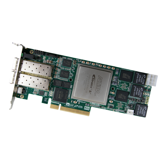
Users can refer to this figure for relative location of the connectors and key components. Figure 2-1 The TR5-Lite Board (Top) TR5-Lite User Manual www.terasic.com June 20, 2018... -
Page 14: Configuration , Status And Setup
Launch Quartus II programmer and make sure the USB-Blaster (or USB-Blaster II) is detected. In Quartus II Programmer, add the configuration bit stream file (.sof), check the associated “Program/Configure” item, and click “Start” to start FPGA programming. TR5-Lite User Manual www.terasic.com June 20, 2018... - Page 15 SW3.1 PCIE_PRSNT2n_x1 Off: Disable x1 presence detect On : Enable x4 presence detect SW3.2 PCIE_PRSNT2n_x4 Off: Disable x4 presence detect On : Enable x8 presence detect SW3.3 PCIE_PRSNT2n_x8 Off: Disable x8 presence detect TR5-Lite User Manual www.terasic.com June 20, 2018...
- Page 16 Selecting Default Factory FPGA Configuration or User-defined Configuration Users can select loading from default factory hardware or user-defined hardware through the use of SW1. The settings for the configurations are shown in Table 2-3. TR5-Lite User Manual www.terasic.com June 20, 2018...
-
Page 17: General User Input /Output
Stratix V GX device. Each push-button provides a high logic level or a low logic level when it is not pressed or pressed, respectively. Table 2-4 lists the board references, signal names and their corresponding Stratix V GX device pin numbers. TR5-Lite User Manual www.terasic.com June 20, 2018... - Page 18 Schematic Stratix IV GX Description Reference Signal Name Standard Pin Number SLIDE_SW0 When the switch is in the ON position, a 2.5-V PIN_E33 logic 0 is selected. SLIDE_SW1 2.5-V PIN_D33 User-Defined LEDs TR5-Lite User Manual www.terasic.com June 20, 2018...
-
Page 19: Temperature Sensor And Fan Control
Table 2-7 Temperature Sensor Pin Assignments, Schematic Signal Names, and Functions Schematic Stratix IV GX Pin Description I/O Standard Signal Name Number Positive pin of temperature diode in TEMPDIODEp 2.5-V PIN_P6 Stratix V TR5-Lite User Manual www.terasic.com June 20, 2018... -
Page 20: Clock Circuit
A clock buffer is used to duplicate the 50 MHz oscillator, so each bank of FPGA I/O bank 3/4/7/8 has two clock inputs. The two programming oscillators are low-jitter oscillators which are used to provide special and high quality clock signals for high-speed transceivers. TR5-Lite User Manual www.terasic.com June 20, 2018... -
Page 21: Rs-422 Serial Port
Figure 2-7 shows the RS-422 block diagram of the development board. The full-duplex LTC28255 is used to translate the RS-422 signal, and the 1394 is used as an external connector for the RS-422 signal. TR5-Lite User Manual www.terasic.com June 20, 2018... -
Page 22: Flash Memory
Internal Termination Resistance Enable. A high input will connect a RS422_TE PIN_AL23 termination resistor (120Ω typical) between pins A and B. The development board has two 1Gb CFI-compatible synchronous flash devices for non-volatile TR5-Lite User Manual www.terasic.com June 20, 2018... - Page 23 Address bus 2.5-V PIN_AG32 FSM_A5 Address bus 2.5-V PIN_AF32 FSM_A6 Address bus 2.5-V PIN_AV34 FSM_A7 Address bus 2.5-V PIN_AM31 FSM_A8 Address bus 2.5-V PIN_AP33 FSM_A9 Address bus 2.5-V PIN_AF34 FSM_A10 Address bus 2.5-V PIN_AR31 TR5-Lite User Manual www.terasic.com June 20, 2018...
- Page 24 Data bus 2.5-V PIN_BB32 FSM_D18 Data bus 2.5-V PIN_BB30 FSM_D19 Data bus 2.5-V PIN_BA31 FSM_D20 Data bus 2.5-V PIN_AW30 FSM_D21 Data bus 2.5-V PIN_BA30 FSM_D22 Data bus 2.5-V PIN_AL29 FSM_D23 Data bus 2.5-V PIN_AR29 TR5-Lite User Manual www.terasic.com June 20, 2018...
-
Page 25: Ddr3 Sdram
I/O banks on the bottom edge of the FPGA. The DDR3 devices shipped with this board are running at 667 MHz, for a total theoretical bandwidth of over 42.68 Gbps. Figure 2-9 shows the connections between the DDR3 and Stratix V GX FPGA. TR5-Lite User Manual www.terasic.com June 20, 2018... - Page 26 Differential 1.5-V SSTL Class I PIN_AG12 DDR3A_QDS_n0 Data Strobe n[0] Differential 1.5-V SSTL Class I PIN_AH12 DDR3A_QDS1 Data Strobe p[1] Differential 1.5-V SSTL Class I PIN_AU10 DDR3A_QDS_n1 Data Strobe n[1] Differential 1.5-V SSTL Class I PIN_AV11 TR5-Lite User Manual www.terasic.com June 20, 2018...
- Page 27 I/O Standard Signal Name Number DDR3B_DQ0 Data [0] SSTL-15 Class I PIN_AN20 DDR3B_DQ1 Data [1] SSTL-15 Class I PIN_AL18 DDR3B_DQ2 Data [2] SSTL-15 Class I PIN_AN19 DDR3B_DQ3 Data [3] SSTL-15 Class I PIN_AP19 TR5-Lite User Manual www.terasic.com June 20, 2018...
- Page 28 Bank Address [2] SSTL-15 Class I PIN_AV14 DDR3B_CK Clock p0 Differential 1.5-V SSTL Class I PIN_BC19 DDR3B_CK_n Clock n0 Differential 1.5-V SSTL Class I PIN_BD19 DDR3B_CKE0 Clock Enable pin 0 SSTL-15 Class I PIN_BD17 TR5-Lite User Manual www.terasic.com June 20, 2018...
-
Page 29: Qdrii+ Sram
PIN_K14 QDRIIA_A13 Address bus[13] 1.8-V HSTL Class I PIN_L15 QDRIIA_A14 Address bus[14] 1.8-V HSTL Class I PIN_J16 QDRIIA_A15 Address bus[15] 1.8-V HSTL Class I PIN_K16 QDRIIA_A16 Address bus[16] 1.8-V HSTL Class I PIN_F13 TR5-Lite User Manual www.terasic.com June 20, 2018... - Page 30 Read Data bus[16] 1.8-V HSTL Class I PIN_P12 QDRIIA_Q17 Read Data bus[17] 1.8-V HSTL Class I PIN_R12 QDRIIA_BWS_n0 Byte Write select[0] 1.8-V HSTL Class I PIN_R13 QDRIIA_BWS_n1 Byte Write select[1] 1.8-V HSTL Class I PIN_P14 TR5-Lite User Manual www.terasic.com June 20, 2018...
- Page 31 Write data bus[2] 1.8-V HSTL Class I PIN_B19 QDRIIB_D3 Write data bus[3] 1.8-V HSTL Class I PIN_L20 QDRIIB_D4 Write data bus[4] 1.8-V HSTL Class I PIN_E18 QDRIIB_D5 Write data bus[5] 1.8-V HSTL Class I PIN_D18 TR5-Lite User Manual www.terasic.com June 20, 2018...
- Page 32 Write Port Select 1.8-V HSTL Class I PIN_A17 QDRIIB_DOFF_n PLL Turn Off 1.8-V HSTL Class I PIN_B14 On-Die Termination QDRIIB_ODT 1.8-V HSTL Class I PIN_C15 Input QDRIIB_QVLD Valid Output Indicator 1.8-V HSTL Class I PIN_C16 TR5-Lite User Manual www.terasic.com June 20, 2018...
- Page 33 Write data bus[12] 1.8-V HSTL Class I PIN_U20 QDRIIC_D13 Write data bus[13] 1.8-V HSTL Class I PIN_V20 QDRIIC_D14 Write data bus[14] 1.8-V HSTL Class I PIN_H21 QDRIIC_D15 Write data bus[15] 1.8-V HSTL Class I PIN_G22 TR5-Lite User Manual www.terasic.com June 20, 2018...
- Page 34 Table 2-16 QDRII+ SRAM D Pin Assignments, Schematic Signal Names, and Functions Schematic Stratix IV GX Pin Description I/O Standard Signal Name Number QDRIID_A0 Address bus[0] 1.8-V HSTL Class I PIN_U26 QDRIID_A1 Address bus[1] 1.8-V HSTL Class I PIN_T27 TR5-Lite User Manual www.terasic.com June 20, 2018...
- Page 35 Read Data bus[1] 1.8-V HSTL Class I PIN_E30 QDRIID_Q2 Read Data bus[2] 1.8-V HSTL Class I PIN_R28 QDRIID_Q3 Read Data bus[3] 1.8-V HSTL Class I PIN_W29 QDRIID_Q4 Read Data bus[4] 1.8-V HSTL Class I PIN_V29 TR5-Lite User Manual www.terasic.com June 20, 2018...
- Page 36 QDRIID_WPS_n 1.8-V HSTL Class I PIN_P30 QDRIID_DOFF_n PLL Turn Off 1.8-V HSTL Class I PIN_G31 On-Die Termination QDRIID_ODT 1.8-V HSTL Class I PIN_D32 Input Valid Output Indicator 1.8-V HSTL Class I QDRIID_QVLD PIN_E32 TR5-Lite User Manual www.terasic.com June 20, 2018...
-
Page 37: Spf
Signal loss indicator 2.5V PIN_AW24 SPFA_MOD0_PRSNT_n Module present 2.5V PIN_BA25 SPFA_MOD1_SCL Serial 2-wire clock 2.5V PIN_BA24 SPFA_MOD2_SDA Serial 2-wire data 2.5V PIN_BB26 SPFA_RATSEL0 Rate select 0 2.5V PIN_AY25 SPFA_RATSEL1 Rate select 1 2.5V PIN_AV25 TR5-Lite User Manual www.terasic.com June 20, 2018... -
Page 38: Pci Express
The power of the board can be sourced entirely from the PCI Express edge connector when installed into a PC motherboard. It is strongly recommended that users connect the PCIe external power connector to 6-pin 12V DC power connector in the TR5-Lite to avoid FPGA damage due to TR5-Lite User Manual www.terasic.com June 20, 2018... - Page 39 PIN_AL41 PCIE_TX_n5 Add-in card transmit bus 1.4-V PCML PIN_AL42 PCIE_TX_p6 Add-in card transmit bus 1.4-V PCML PIN_AJ41 PCIE_TX_n6 Add-in card transmit bus 1.4-V PCML PIN_AJ42 PCIE_TX_p7 Add-in card transmit bus 1.4-V PCML PIN_AG41 TR5-Lite User Manual www.terasic.com June 20, 2018...
-
Page 40: Sata
(such as hard drives, optical drives, and solid-state disks). Supporting a storage interface is just one of many different applications an FPGA can be used in storage appliances. The Stratix V GX device can bridge different protocols such as bridging simple bus I/Os TR5-Lite User Manual www.terasic.com June 20, 2018... - Page 41 Differential receive data input SATA_HOST_RX_p0 1.4-V PCML PIN_AP2 after DC blocking capacitor Differential receive data input SATA_HOST_RX_n0 1.4-V PCML PIN_AP1 after DC blocking capacitor SATA_REFCLK_ p Reference Clock HCSL PIN_AF7 SATA_REFCLK_ n Reference Clock HCSL PIN_AF6 TR5-Lite User Manual www.terasic.com June 20, 2018...
-
Page 42: Chapter 3 System Builder
Board damaged for wrong pin/bank voltage assignment. Board malfunction caused by wrong device connections or missing pin counts for connected ends. Performance dropped because of improper pin assignments TR5-Lite User Manual www.terasic.com June 20, 2018... -
Page 43: General Design Flow
The Quartus II setting file contains information such as FPGA device type, top-level pin assignment, and I/O standard for each user-defined I/O pin. Finally, Quartus II programmer must be used to download SOF file to TR5-Lite board using JTAG interface. TR5-Lite User Manual www.terasic.com June 20, 2018... -
Page 44: Using Tr5-Lite System Builder
System CD. Users can copy the whole folder to a host computer without installing the utility. Before using the TR5-Lite System Builder, execute the TR5_Lite_SystemBuilder.exe on the host computer as appears in Figure 3-2. TR5-Lite User Manual www.terasic.com June 20, 2018... - Page 45 System Configuration Under System Configuration users are given the flexibility of enabling their choice of components on the TR5-Lite as shown in Figure 3-4. Each component of the TR5-Lite is listed where users can TR5-Lite User Manual www.terasic.com June 20, 2018...
- Page 46 Note. If users need to dynamically change the frequency, they would need to modify the generated TR5-Lite User Manual www.terasic.com June 20, 2018...
- Page 47 Figure 3-6. Users can save the current board configuration information into a .cfg file and load it to the TR5-Lite System Builder. Figure 3-6 Project Settings Project Generation TR5-Lite User Manual www.terasic.com June 20, 2018...
- Page 48 SRAM Object File (.sof). For SI570, the Controller will be instantiated in the Quartus II top-level file as listed below: For CDCM61004, the Controller will be instantiated in the Quartus II top-level file as listed below: TR5-Lite User Manual www.terasic.com June 20, 2018...
- Page 49 If dynamic configuration for the oscillator is required, users need to modify the code according to users’ desired behavior. TR5-Lite User Manual www.terasic.com June 20, 2018...
-
Page 50: Flash Programming
For user application, user hardware must be stored with start address 0x020C0000, and the user’s software is suggested to be stored with start address 0x04940000. The NIOS II EDS tool nios-2-flash-programmer is used for programming the flash. Before programming, users need to TR5-Lite User Manual www.terasic.com June 20, 2018... -
Page 51: Fpga Configure Operation
Top batch file to download TR5_LITE_PFL.sof and launch batch flash_program_bashrc_ub2 flash_program_bashrc_ub2 Translate .sof and .elf into .flash and programming flash with the generated .flash file TR5_LITE_golden_top.sof Hardware design file for Hello Demo TR5-Lite User Manual www.terasic.com June 20, 2018... - Page 52 0x00, as shown in Figure 4-3. 2. In NIOS II processor options, select FLASH as reset vector memory and specify 0x04940000 as reset vector, as shown in Figure 4-4. TR5-Lite User Manual www.terasic.com June 20, 2018...
-
Page 53: Restore Factory Settings
This section describes how to restore the original factory contents to the flash memory device on the FPGA development board. Perform the following instructions: 1. Make sure the Nios II EDS and USB-Blaster II driver are installed. TR5-Lite User Manual www.terasic.com June 20, 2018... - Page 54 The NIOS II EDS tool nios-2-flash-programmer programs the Flash based on the Parallel Flasher Loader design in the FPGA. The Parallel Flash Loader design is included in the default code TR5_Lite_PFL and the source code is available in the folder Demonstrations/TR5_Lite_PFL in System CD. TR5-Lite User Manual www.terasic.com June 20, 2018...
-
Page 55: Chapter 5 Programmable Oscillator
644.53125MHz or 322.265625MHz from the Si570. Figure 5-1 shows the block diagram of SI570 device. Users can modify the value of the three registers RFREQ, HS_DIV, and N1 to generate the desired output frequency. TR5-Lite User Manual www.terasic.com June 20, 2018... - Page 56 12. Unfreeze the DCO and assert the NewFreq bit (bit 6 of Register 135). The I2C address of Si570 is zero and it supports fast mode operation whose transfer rate is up to 400 kbps. Table 5-1 shows the register table for Si570. TR5-Lite User Manual www.terasic.com June 20, 2018...
- Page 57 Table 5-2 Si570 Register Table Output HS_DIV HS_DIV REF_CLK Frequency Register Register Register (MHz) Setting Setting Setting 0000101 02F40135A9(hex) 0000011 0302013B65(hex) 156.25 0000011 0313814290(hex) 0000001 0302013B65(hex) 312.5 0000001 0313814290(hex) 322.265625 0000011 02D1E127AF(hex) 644.53125 0000001 02D1E127AF(hex) TR5-Lite User Manual www.terasic.com June 20, 2018...
- Page 58 12 GigE PCI Express GigE 312.5 XGMII 10 GigE The both values of PRESCALER DIVIDER and FEEDBACK DIVIDER can be specified by the PR0 and PR1 control pins according to the following table: TR5-Lite User Manual www.terasic.com June 20, 2018...
-
Page 59: Xample By Rtl
Recalibration process. In the TR5-Lite, the required output type is LVDS, so always set OS0 and SO1 to 0 and 1, respectively. In this section we will demonstrate how to use the Terasic SI570 Controller implemented in Verilog to control the SI570 programmable oscillator on the TR5-Lite board. This controller IP can configure the SI570 to output a clock with a specific frequency via I2C interface. - Page 60 Secondly, the clock_divider block will divide system clock (50Mhz) into 97.6Khz which is used as I2C interface clock of i2c_bus_controller. Finally, the initial_config block will generate a control signal to drive i2c_reg_controller which allows the SI570 controller to configure SI570 based on default settings. TR5-Lite User Manual www.terasic.com June 20, 2018...
- Page 61 For example, setting “iFREQ_MODE” as 3’b110 corresponding frequencies are listed in Table 5-4. will configure SI570 to output 655.53 MHz clock. Table 5-4 SI570 Controller Frequency Setting iFREQ MODE Setting SI570 Clock Frequency(MHz) 3'b000 3'b001 TR5-Lite User Manual www.terasic.com June 20, 2018...
- Page 62 Modify Clock Parameter For Your Own Frequency If all the six clock frequencies are not user desired, user can perform the following steps to modify SI570 controller. 1. Open i2c_reg_controller.v 2. Locate the Verilog code shown below: TR5-Lite User Manual www.terasic.com June 20, 2018...
- Page 63 = 4'b0101 ; new_n1 = 8'b0000_0100 ; fdco = 28'h004_E200 ; 3'h4 : //312.5Mhz begin new_hs_div = 4'b0100 ; new_n1 = 8'b0000_0100 ; fdco = 28'h004_E200 ; 3'h5 : //322.265625Mhz begin TR5-Lite User Manual www.terasic.com June 20, 2018...
- Page 64 2. 4 <= new_hs_div <= 11 3. 1 <= new_n1 < =128 For example, you want to get a 133.5 mhz clock, then fdco = 133.5 x 4 x 10 x 64 = 341760d = 0x53700 TR5-Lite User Manual www.terasic.com June 20, 2018...
- Page 65 Figure 5-5 Programmable Oscillator Calculator tool In addition, if the user doesn’t want Si570 controller to configure Si570 as soon as the FPGA configuration finishes, users can change settings in Si570_controller.v, shown below. TR5-Lite User Manual www.terasic.com June 20, 2018...
- Page 66 Demonstration Setup Make sure Quartus II is installed on your PC. Connect the USB Blaster cable to the TR5-Lite board and host PC. Install the USB Blaster driver if necessary. TR5-Lite User Manual www.terasic.com June 20, 2018...
-
Page 67: And Cdcm Programming By Ios Ii
Si570 are controlled through I2C interface. The Nios II program toggles the PIO controller to implement the I2C protocol. The CDCM 61004 is programmed through the PIO directly. The Nios II program is running in the on-chip memory. TR5-Lite User Manual www.terasic.com June 20, 2018... - Page 68 FPGA temperature, and the local temperature the board temperature where the temperature sensor located. In the external PLL programming test, the program will program the PLL first, then use TERASIC QSYS custom CLOCK_COUNTER IP to count the clock count in a specified period to check whether the output frequency is changed as demanded.
- Page 69 Batch File for USB-Blaster (II): test.bat, test_bashrc (test_ub2.bat, test_bashrc_ub2) FPGA Configure File: TR5_LITE_gondlen_top.sof Nios II Program: Nios_DEMO.elf Demonstration Setup Make sure Quartus II and Nios II are installed on your PC. TR5-Lite User Manual www.terasic.com June 20, 2018...
- Page 70 For programming PLL Si570 test, please input key ‘2’ and press ‘Enter’ in the nios-terminal first, then select the desired output frequency , as shown in Figure 5-10. Figure 5-8 Temperature Demo TR5-Lite User Manual www.terasic.com June 20, 2018...
- Page 71 Figure 5-9 CDCM 61004 Demo Figure 5-10 Si570 Demo TR5-Lite User Manual www.terasic.com June 20, 2018...
-
Page 72: Memory Reference Design
Altera’s “QDRII and QDRII+ SRAM Controller with UniPHY” IP to implement a memory test function. In the design, the four QDRII controllers share the same PLL/DLL/OCT due to limited DLL numbers in the FPGA. TR5-Lite User Manual www.terasic.com June 20, 2018... - Page 73 (the same sequence as the write data). Test control signals for four QDRII+ SRAMs will generate from BUTTON0 and four LEDs will indicate the test results of four QDRII+ SRAMs. TR5-Lite User Manual www.terasic.com June 20, 2018...
- Page 74 Make sure Quartus II is installed on your PC. Connect the USB Blaster cable (or USB-Blaster II cable) to the TR5_Lite board and host PC. Install the USB-Blaster driver if necessary. TR5-Lite User Manual www.terasic.com June 20, 2018...
-
Page 75: Ddr3 Sdram Test
(DLLs), phase-locked loops (PLLs), and on-chip termination (OCT). The controller uses 50 MHz as a reference clock, generates one 666.667 MHz clock as memory clock, and generates one quarter-rate system clock 166.666 MHz for the controller itself. TR5-Lite User Manual www.terasic.com June 20, 2018... - Page 76 2. Setup correct parameters in DDR3 controller dialog. 3. Perform “Analysis and Synthesis” by selecting from the Quartus II menu: ProcessStartStart Analysis & Synthesis. 4. Run the TCL files generated by DDR3 IP by selecting from the Quartus II menu: TR5-Lite User Manual www.terasic.com June 20, 2018...
- Page 77 DDR3 (A) and DDR3 (B) have passed the test, respectively. Table 4-2 lists the LED indicators. If LED3 is not blinking, it means the 50MHz clock source is not working. TR5-Lite User Manual www.terasic.com June 20, 2018...
-
Page 78: Ddr3 Sdram Test By Ios Ii
666.667/4=166.666 MHz for those host controllers, e.g. Nios II processor, accessing the SDRAM. In the QSYS, Nios II and the On-Chip Memory are designed running with the 166.666 MHz clock, and the Nios II program is running in the on-chip memory. TR5-Lite User Manual www.terasic.com June 20, 2018... - Page 79 2. Setup correct parameters in DDR3 controller dialog. 3. Perform “Analysis and Synthesis” by clicking Quartus menu: ProcessStartStart Analysis & Synthesis. 4. Run the TCL files generated by DDR3 IP by clicking Quartus menu: ToolsTCL Scripts… TR5-Lite User Manual www.terasic.com June 20, 2018...
- Page 80 Demo Batch File Folder: Nios_DDR3\demo_batch\DDR3_A_667HZ or Nios_DDR3\demo_batch\DDR3_B_667MHZ The demo batch file includes following files: Batch File for USB-Blaseter (II): test.bat, test_bashrc (test_ub2.bat, test_bashrc_ub2) FPGA Configure File: TR5_LITE_gondlen_top.sof Nios II Program: TEST_DDR3.elf TR5-Lite User Manual www.terasic.com June 20, 2018...
- Page 81 The program will display progressing and result information, as shown in Figure 6-4. Figure 6-4 Display Progress and Result Information for the DDR3 Demonstration TR5-Lite User Manual www.terasic.com June 20, 2018...
-
Page 82: Chapter 7 Transceiver Verification
6.0 Gbps: SATA Host 8.0 Gbps: PCIe Channel 0~7 To enable an external loopback of transceiver channels, specific loopback fixtures are required. Some fixtures may be proprietary to Terasic. For SFP+ loopback, optical SFP+ loopback fixtures are required. Figure 7-1 shows the optical SFP+ loopback fixture. - Page 83 F igure 7-2 shows the SATA loopback fixture. Figure 7-2 SATA Loopback Fixture F igure 7-3 shows the Terasic PCIe loopback fixture. 1 7 6 H 1 7 4 H Figure 7-3 PCIe Loopback Fixture F igure 7-4 shows the FPGA board with all transceiver loopback fixtures installed.
-
Page 84: Testing
10. To terminate the test, press one of the BUTTON0~1 buttons on the FPGA board. The loopback test will terminate, and the test summary will be shown in the Nios-Terminal, as shown in F igure 7-5. 1 7 9 H 1 7 7 H TR5-Lite User Manual www.terasic.com June 20, 2018... - Page 85 Figure 7-5 Transceiver Loopback Test in Progress TR5-Lite User Manual www.terasic.com June 20, 2018...
-
Page 86: Additional Information
Additional Information Here are the addresses where you can get help if you encounter problems: Terasic Technologies 9F., No.176, Sec.2, Gongdao 5th Rd, East Dist, HsinChu City, 30070. Taiwan, 30070 Email: support@terasic.com Web: www.terasic.com TR5-Lite Web: tr5-lite.terasic.com Date Version Changes 2012.4...
Need help?
Do you have a question about the TR-5 Lite FPGA and is the answer not in the manual?
Questions and answers