Table of Contents
Advertisement
Quick Links
Advertisement
Table of Contents

Related Manuals for Terasic ALTERA MAX 10 NEEK


Summary of Contents for Terasic ALTERA MAX 10 NEEK
- Page 1 MAX 10 NEEK User www.terasic.com February 4, 2016 Manual...
-
Page 2: Table Of Contents
5.3 ADC Potentiometer ........................55 5.4 DAC Demonstration ......................... 57 5.5 ADC/MIC/LCD Demonstration ....................60 5.6 HDMI RX Demonstration ......................63 Chapter 6 NIOS Based Example Codes ............67 MAX 10 NEEK www.terasic.com February 4, 2016... - Page 3 8.2 Using Dual Compressed Images .................... 114 8.3 Nios II Load In Single Boot Image ..................117 Chapter 9 Appendix ..................120 Revision History ........................... 120 Copyright Statement ........................120 MAX 10 NEEK www.terasic.com February 4, 2016...
-
Page 4: Max 10 Neek Development Kit
Chapter 1 MAX 10 NEEK Development Kit The MAX 10 NEEK from Terasic is a full featured embedded evaluation kit based upon the MAX10 family of Altera FPGAs. It offers a comprehensive design environment with everything embedded developers need to create a processing based system. The MAX 10 NEEK delivers an integrated platform that includes hardware, design tools, intellectual property and reference designs for developing a wide range of audio, video and many other exciting applications. -
Page 5: Max 10 Neek System Cd
The MAX 10 NEEK System CD contains all the documents and supporting materials associated with MAX 10 NEEK, including the user manual, system builder, reference designs, and device datasheets. Users can download this system CD from the link: http://cd-max10-neek.terasic.com. Here are the addresses where you can get help if you encounter any problems: ... -
Page 6: Introduction Of The Max 10 Neek Board
It depicts the layout of the board and indicates the Figure 2-1 location of the connectors and key components. Figure 2-1 MAX 10 NEEK development board (top view) MAX 10 NEEK www.terasic.com February 4, 2016... - Page 7 HDMI RX, incorporates HDM v1.4a features, including 3D video supporting 800x480 7.0 inch Color LCD with 5-point Capacitive-touch Gigabit Ethernet PHY with RJ45 connector UART to USB, USB Mini-B connector 8M pixel MIPI CS2 color camera input MAX 10 NEEK www.terasic.com February 4, 2016...
-
Page 8: Block Diagram Of The Max 10 Neek Board
All the connections are established through the MAX Figure 2-3 10 FPGA device to provide maximum flexibility for users. Users can configure the FPGA to implement any system design. Figure 2-3 Block diagram of MAX 10 NEEK MAX 10 NEEK www.terasic.com February 4, 2016... - Page 9 Gigabit Ethernet PHY with RJ45 connector UART to USB, USB Mini-B connector PS/2 mouse/keyboard connector 2x6 TMD (Terasic Mini Digital) Expansion Header 800x480 7.0 inch Color LCD with 5-point Capacitive-touch 24-bit CD-quality audio CODEC with line-in, line-out jacks ...
- Page 10 Five push-buttons Ten slide switches Ten red user LEDs Two 7-segment displays Ambient light sensor Humidity and temperature sensor Accelerometer Power monitor 5V/3A DC input MAX 10 NEEK www.terasic.com February 4, 2016...
-
Page 11: Using The Max 10 Neek Board
The FPGA device can be configured through JTAG interface on MAX 10 NEEK board, but the JTAG chain must form a closed loop, which allows Quartus II programmer to the detect FPGA device. illustrates the JTAG chain on MAX 10 NEEK board Figure 3-1 MAX 10 NEEK www.terasic.com February 4, 2016... - Page 12 1. Open the Quartus II programmer and click “Auto Detect”, as circled in Figure 3-2 Figure 3-2 Detect FPGA device in JTAG mode 2. Select detected device associated with the board, as circled in Figure 3-3. MAX 10 NEEK www.terasic.com February 4, 2016...
- Page 13 3. FPGA is detected, as shown in Figure 3-4. Figure 3-4 FPGA detected in Quartus programmer 4. Right click on the FPGA device and open the .sof file to be programmed, as highlighted in Figure 3-5 MAX 10 NEEK www.terasic.com February 4, 2016...
- Page 14 Figure 3-5 Open the .sof file to be programmed into the FPGA device 5. Select the .sof file to be programmed, as shown in Figure 3-6. MAX 10 NEEK www.terasic.com February 4, 2016...
- Page 15 Figure 3-6 Select the .sof file to be programmed into the FPGA device 6. Click “Program/Configure” check box and then click “Start” button to download the .sof file into the FPGA device, as shown in Figure 3-7. MAX 10 NEEK www.terasic.com February 4, 2016...
- Page 16 Please refer to Chapter 8: Programming the Configuration Flash Memory (CFM) for the basic programming instruction on the configuration flash memory (CFM). Figure 3-8 High-Level Overview of Internal Configuration for MAX 10 Devices MAX 10 NEEK www.terasic.com February 4, 2016...
-
Page 17: Board Status Elements
Illuminate during data is uploaded from MAX 10 device to PC JTAG_RX through UB2. Illuminate during configuration data is loaded into MAX 10 JTAG_TX device from UB2. Illuminate during transmitting data via USB. Illuminate during receiving data via USB. MAX 10 NEEK www.terasic.com February 4, 2016... -
Page 18: Clock Circuitry
FPGA, the outputs of these two PLLs can drive ADC clock. The associated pin assignment for clock inputs to FPGA I/O pins is listed in Table 3-2. Figure 3-10 Block diagram of the clock distribution on MAX 10 NEEK MAX 10 NEEK www.terasic.com February 4, 2016... -
Page 19: Peripherals Connected To The Fpga
Figure 3-12 Figure 3-11 Connections between the push-buttons and the MAX 10 FPGA MAX 10 NEEK www.terasic.com February 4, 2016... - Page 20 LED on or off, respectively. shows the connections between LEDs and MAX Figure 3-14 10 FPGA. list the pin assignment of user push-buttons, Table 3-3, Figure 3-14 Table 3-9 switches, and LEDs. MAX 10 NEEK www.terasic.com February 4, 2016...
- Page 21 PIN_H21 Slide Switch[9] 1.5V Table 3-5 Pin Assignment of LEDs Signal Name FPGA Pin No. Description I/O Standard LEDR[0] PIN_C2 LEDR [0] 3.3V LEDR[1] PIN_B3 LEDR [1] 3.3V LEDR[2] PIN_A3 LEDR [2] 3.3V MAX 10 NEEK www.terasic.com February 4, 2016...
- Page 22 Seven Segment Digit 0[1] 3.3V HEX0[2] PIN_C6 Seven Segment Digit 0[2] 3.3V HEX0[3] PIN_A6 Seven Segment Digit 0[3] 3.3V HEX0[4] PIN_F7 Seven Segment Digit 0[4] 3.3V HEX0[5] PIN_D7 Seven Segment Digit 0[5] 3.3V MAX 10 NEEK www.terasic.com February 4, 2016...
- Page 23 Figure 3-16 Connections between the power monitor chip and the MAX 10 FPGA Table 3-5 Pin Assignment of Power Monitor I2C bus Signal Name FPGA Pin No. Description I/O Standard PM_I2C_SCL PIN_E8 Power Monitor SCL 3.3V PM_I2C_SDA PIN_E9 Power Monitor SDA 3.3V MAX 10 NEEK www.terasic.com February 4, 2016...
- Page 24 The board has one 2x6 TMD (Terasic Mini Digital) expansion header. The TMD header has 8 digital GPIO user pins connected to the MAX 10 FPGA, two 3.3V power pins and two ground pins. There are two Transient Voltage Suppressor diode arrays used to implement ESD protection for 8 GPIO user pins..
- Page 25 Texas Instruments INA159 gain of 0.2 level translation difference amplifier, then the amplifier’s outputs are fed to dedicated single-ended analog input pins for MAX 10 build-in ADC1 and ADC2 respectively. With the amplifiers, the analog input of two SMAs MAX 10 NEEK www.terasic.com February 4, 2016...
- Page 26 8 bit (128Mx8) device. The DDR3 devices shipped with this board are running at 300MHz with the soft IP of MAX 10 external memory interface solution. shows the connections Figure 3-20 between the DDR3 and MAX 10 FPGA. shows the DDR3 interface pin assignments. Table 3-8 MAX 10 NEEK www.terasic.com February 4, 2016...
- Page 27 SSTL-15 Class I DDR3_A[14] PIN_C20 DDR3 Address[14] SSTL-15 Class I DDR3_BA[0] PIN_W22 DDR3 Bank Address[0] SSTL-15 Class I DDR3_BA[1] PIN_Y21 DDR3 Bank Address[1] SSTL-15 Class I DDR3_BA[2] PIN_Y22 DDR3 Bank Address[2] SSTL-15 Class I MAX 10 NEEK www.terasic.com February 4, 2016...
- Page 28 Class I DDR3_ODT PIN_V22 DDR3 On-die Termination SSTL-15 Class I DDR3_RAS_n PIN_N18 DDR3 Row Address Strobe SSTL-15 Class I DDR3_RESET_n PIN_B22 DDR3 Reset SSTL-15 Class I DDR3_WE_n PIN_W19 DDR3 Write Enable SSTL-15 Class I MAX 10 NEEK www.terasic.com February 4, 2016...
- Page 29 88E1111 chip with integrated 10/100/1000 Mbps Gigabit Ethernet transceiver support GMII/MII/RGMII/TBI MAC interfaces. shows the connections between the MAX 10 Figure 3-22 FPGA, Ethernet PHY, and RJ-45 connector. The pin assignment associated to Gigabit Ethernet MAX 10 NEEK www.terasic.com February 4, 2016...
- Page 30 GMII and MII receive data[2] 2.5V NET_RX_D[3] PIN_B11 GMII and MII receive data[3] 2.5V NET_RX_CLK PIN_J10 GMII and MII receive clock 3.3V NET_RST_n PIN_C14 Hardware Reset Signal 2.5V NET_MDIO PIN_E12 Management Data 2.5V MAX 10 NEEK www.terasic.com February 4, 2016...
- Page 31 Video Pixel Output Port 3.3V HDMI_RX_D1 PIN_AB9 Video Pixel Output Port 3.3V HDMI_RX_D2 PIN_Y10 Video Pixel Output Port 3.3V HDMI_RX_D3 PIN_AA10 Video Pixel Output Port 3.3V HDMI_RX_D4 PIN_AB10 Video Pixel Output Port 3.3V MAX 10 NEEK www.terasic.com February 4, 2016...
- Page 32 MIPI camera module, MIPI CSI-2 to parallel bridge device Figure 3-24 and MAX 10 FPGA. The pin assignment associated to this MIPI CSI-2 to parallel interface is shown in Table 3-12. MAX 10 NEEK www.terasic.com February 4, 2016...
- Page 33 Parallel Port Data 3.3V MIPI_PIXEL_D[16] PIN_AB7 Parallel Port Data 3.3V MIPI_PIXEL_D[17] PIN_Y8 Parallel Port Data 3.3V MIPI_PIXEL_D[18] PIN_AA8 Parallel Port Data 3.3V MIPI_PIXEL_D[19] PIN_AA7 Parallel Port Data 3.3V MIPI_PIXEL_D[20] PIN_Y7 Parallel Port Data 3.3V MAX 10 NEEK www.terasic.com February 4, 2016...
- Page 34 Figure 3-25 Connections between 7.0 inch color LCD and MAX 10 FPGA Table 3-13 Pin Assignment of 7.0 inch LCD interface Signal Name FPGA Pin No. Description I/O Standard MTL2_R[0] PIN_U5 Red Data (LSB) 3.3V MTL2_R[1] PIN_U4 Red Data 3.3V MAX 10 NEEK www.terasic.com February 4, 2016...
- Page 35 1 and pin 2 of J13 to select on-board microphone, short pin 3 and pin 4 to select pin 16 of 2x10 header J7. shows the connection of 2x10 ADC header and MAX 10 FPGA. Figure 3-26 MAX 10 NEEK www.terasic.com February 4, 2016...
- Page 36 MAX 10 NEEK simultaneously by a PS/2 Y-Cable, as shown in Figure 3-28. Instructions on how to use PS/2 mouse and/or keyboard can be found on various educational MAX 10 NEEK www.terasic.com February 4, 2016...
- Page 37 The board provides a Texas Instruments DAC8551 16-bit digital-to-analog converter (DAC). It is a small, low power, voltage output DAC. The DAC8551 used a versatile 3-wire serial interface that operates at clock rates to 30MHz and is compatible with standard SPI, QSPI, Microwire and DSP MAX 10 NEEK www.terasic.com February 4, 2016...
- Page 38 \Datasheets\UART TO USB of MAX 10 NEEK system CD. shows the connections Figure 3-30 between the MAX 10 FPGA, FT232R chip, and the USB Mini-B connector. lists the Figure 3-34 pin assignment of UART interface connected to the MAX 10 FPGA. MAX 10 NEEK www.terasic.com February 4, 2016...
- Page 39 APDS-9301 to the MAX 10 FPGA. Figure 3-35 lists the Ambient Light Sensor pin assignments. Table 3-17 Figure 3-31 hows the connections between the MAX 10 FPGA and Ambient Light Sensor MAX 10 NEEK www.terasic.com February 4, 2016...
- Page 40 Signal Name FPGA Pin No. Description I/O Standard RH_TEMP_I2C_SCL PIN_Y18 I2C Clock for HDC1000 Sensor 3.3V RH_TEMP_I2C_SDA PIN_W18 I2C Data for HDC1000 Sensor 3.3V RH_TEMP_DRDY_n PIN_Y19 Data ready input from HDC1000 Sensor 3.3V MAX 10 NEEK www.terasic.com February 4, 2016...
- Page 41 SPI enable, I2C/SPI mode selection: 1: 2.5V SPI idle mode/I2C communication enabled, 0: SPI communication mode/I2C disabled GSENSOR_SCLK PIN_A15 I2C serial clock/SPI serial port clock 2.5V GSENSOR_INT1 PIN_B15 Interrupt pin 1 2.5V GSENSOR_INT2 PIN_D17 Interrupt pin 2 2.5V MAX 10 NEEK www.terasic.com February 4, 2016...
- Page 42 I/O Standard SD_CLK PIN_A16 SD Clock 2.5V SD_CMD PIN_C18 SD Command Line 2.5V SD_DATA[0] PIN_A17 SD Data[0] 2.5V SD_DATA[1] PIN_A18 SD Data[1] 2.5V SD_DATA[2] PIN_B17 SD Data[2] 2.5V SD_DATA[3] PIN_C17 SD Data[3] 2.5V MAX 10 NEEK www.terasic.com February 4, 2016...
- Page 43 The MAX 10 NEEK is powered by Linear Technology’s power solution which provides high-efficiency power management for FPGAs and SoCs. shows the power tree of Figure 3-35 MAX 10 NEEK. Figure 3-35 Power tree of MAX 10 NEEK MAX 10 NEEK www.terasic.com February 4, 2016...
-
Page 44: Neek10 System Builder
Quartus II project files, Quartus II setting file, top-level design file, Synopsis design constraint file, and the pin assignment document. The top-level design file contains a top-level Verilog HDL wrapper for users to add their own MAX 10 NEEK www.terasic.com February 4, 2016... - Page 45 After the compilation is successful, users can download the .sof file to the developmenet board via JTAG interface using the Qaurtus II programmer. Figure 4-1 Design flow of building a project from the beginning to the end MAX 10 NEEK www.terasic.com February 4, 2016...
-
Page 46: Using Neek10 System Builder
Figure 4-2 The GUI of NEEK10 System Builder Enter Project Name The project name entered in the circled area, as shown in 4-3, will be assigned automatically Figure as the name of the top-level design entity. MAX 10 NEEK www.terasic.com February 4, 2016... - Page 47 4-4. If a component is enabled, the NEEK10 System Figure Builder will automatically generate its associated pin assignment, including the pin name, pin location, pin direction, and I/O standard. MAX 10 NEEK www.terasic.com February 4, 2016...
- Page 48 Figure 4-4 List of onboard peripherals in System Configuration Project Settings The NEEK10 System Builder also provides the option to load a setting or save the current board configuration in .cfg file, as shown in Figure 4-5. MAX 10 NEEK www.terasic.com February 4, 2016...
- Page 49 When users press the Generate button, as shown in the NEEK10 System Builder will Figure 4-6, generate the corresponding Quartus II files and documents, as listed in Table 4-1 Files generated by the NEEK10 System Builder: MAX 10 NEEK www.terasic.com February 4, 2016...
- Page 50 Synopsis design constraints file for Quartus II <Project name>.htm Pin assignment document Users can add custom logic into the project and compile the project in Quartus II to generate the SRAM Object File (.sof). MAX 10 NEEK www.terasic.com February 4, 2016...
-
Page 51: Rtl Example Codes
The PS/2 controller samples the data line at the falling edge of the PS/2 clock signal. This is implemented by a shift register, which consists of 33 bits, but be cautious with the clock domain crossing problem. MAX 10 NEEK www.terasic.com February 4, 2016... - Page 52 After the power-on cycle of the PS/2 mouse, it enters into stream mode automatically and disable data transmit unless an enabling instruction is received. shows the waveform while Figure 5-1 communication happening on two lines. Figure 5-1 Waveform of Clock and Data Signals during Data Transmission MAX 10 NEEK www.terasic.com February 4, 2016...
- Page 53 Table 5-1 Description of 7-segment Display and LED Indicators Indicator Name Description LEDR0 Left button press indicator LEDR1 Right button press indicator LEDR2 Middle button press indicator HEX0 Low byte of X/Y displacement HEX1 High byte of X/Y displacement MAX 10 NEEK www.terasic.com February 4, 2016...
-
Page 54: Power Monitor
SW[2:0] and the value will be displayed on the two 7-segments on the NEEK10 board. The unit is in mW Figure 5-2 Block diagram of Power Monitor demonstration MAX 10 NEEK www.terasic.com February 4, 2016... - Page 55 Execute the demo batch file “ test.bat” from the directory \power_monitor\demo_batch. The two 7-segments on the NEE10 board will display mW of the bus chosen in decimal, as Figure 5-3. Figure 5-3 Display power (mW) on the 7-segments and LED MAX 10 NEEK www.terasic.com February 4, 2016...
-
Page 56: Adc Potentiometer
ADC hard IP block in MAX10 device. Figure 5-4 Block diagram of ADC hard IP block This demo uses 2nd ADC of MAX10 on channel 8. The ADC settings are shown in Figure 5-5 MAX 10 NEEK www.terasic.com February 4, 2016... - Page 57 7-segments. Since none of the dot points of two 7-segments is connected to the MAX 10, so HEX1 and HEX0 shows the decimal point and the first digit after the decimal point respectively. Figure 5-6 Block diagram of ADC Potentiometer MAX 10 NEEK www.terasic.com February 4, 2016...
-
Page 58: Dac Demonstration
The analog signal coming out of the DAC SMA connector is connected to the oscilloscope and shown in square wave. Users can switch the SW0~2 to change the frequency MAX 10 NEEK www.terasic.com February 4, 2016... - Page 59 Plug in the 5V adapter to the NEEK10 Board and power it up. Execute the demo batch file “ test.bat” from the directory \ dac_sma\demo_batch. Connect the probe of the oscilliscope to the DAC SMA OUT of the NEEK 10 board and adjust MAX 10 NEEK www.terasic.com February 4, 2016...
- Page 60 When SW[2:0]=000, the square wave frequency is at about 2.6KHz; When SW[2:0]=111, the frequency is about 112KHz. Figure 5-8 Use the oscilloscope to observe the square wave Figure 5-9 Probe DAC SMA OUT from the oscilloscope MAX 10 NEEK www.terasic.com February 4, 2016...
-
Page 61: Adc/Mic/Lcd Demonstration
DAC16 converts the digitized signal in parallel to 16-bit serial format for the DAC chip (DAC8551) to the Line-out via audio codec (TLV320AIC3254). The module LED_METER displays the volume of the sound on the 10 LEDs onboard. MAX 10 NEEK www.terasic.com February 4, 2016... - Page 62 The sound wave from the MIC can be observed on the LCD and probed through DAC SMA OUT from the oscilloscope, or can also connect external speaker to Line-out to hear the sound, 5-12. The volume of the sound from the MIC is displayed digitally on LEDR0~9, as Figure MAX 10 NEEK www.terasic.com February 4, 2016...
- Page 63 5-13. Figure 5-12 The waveform of onboard MIC is displayed on both LCD and oscilloscope. Its sound is played out from the speaker Figure 5-13 LEDR0~9 displays the volume level of onboard MIC MAX 10 NEEK www.terasic.com February 4, 2016...
-
Page 64: Hdmi Rx Demonstration
7”LCD refers to Figure 5-14 Terasic multi-touch panel. HDMI RX(ADV7611) is a chip to decrypt HDMI video and audio data. Before decrypting HDMI data, a proper setting is necessary where HDMIConfig(I2C) module is used to configure the ADV7611 chip. - Page 65 5-16. Audio Codec configuration setting can be divided to either page0 or page1. During the configuration process, you would have to pay attention if the current setting is in page0 or page1. Paying attention to such details can help you set up Audio Codec more efficiently. MAX 10 NEEK www.terasic.com February 4, 2016...
- Page 66 "test.bat" batch file. This will configure the FPGA, download the demo application to the board and start its execution. After it's done, the screen should look like the one shown in Figure 5-17. MAX 10 NEEK www.terasic.com February 4, 2016...
- Page 67 Therefore in that scenario, we would suggest you contact HDCP and apply for authorization. For more details, you can check at http://www.digital-cp.com/. shows the setup of the Figure 5-18 demo. Figure 5-18 The Demo Setup MAX 10 NEEK www.terasic.com February 4, 2016...
-
Page 68: Nios Based Example Codes
Nios II processor is running at 50 MHz. The I2C library is located in the files named I2C_core.cpp and I2C_core.h. The I2C OpenCore IP is located in the folder “ip/i2c_opencores” under the project directory. MAX 10 NEEK www.terasic.com February 4, 2016... - Page 69 Current = (V1-V2) / R SENSE The power consumption can be calculated by the following formula: Power Consumption = V x Current = V x (V1-V2) / R SENSE Figure 6-2 Schematic of current sense MAX 10 NEEK www.terasic.com February 4, 2016...
- Page 70 LTC2990. The control register must be configured properly Figure 6-4 to measure the voltage difference (V1-V2). Bits b[2:0] should be set to ‘110’ for measuring voltage difference (V1-V2) and (V3-V4). Bits [4:3] should be set to 00 for all measurements. MAX 10 NEEK www.terasic.com February 4, 2016...
- Page 71 Figure 6-5 tatus register of LTC2990. Design Tools Quartus II v15.0 64-bit Nios II Eclipse 15.0 Demonstration Source Code Quartus project directory: Demonstrations\power_monitor_nios Nios II Eclipse project workspace: Demonstrations\power_monitor_nios\software MAX 10 NEEK www.terasic.com February 4, 2016...
- Page 72 Execute the demo batch file “ test.bat ” under the folder Demonstrations\power_monitor _nios\demo_batch. Nios II terminal will display the measured power consumption measured, as shown in Figure 6-6. Figure 6-6 Screenshot of power_monitor_nios demo MAX 10 NEEK www.terasic.com February 4, 2016...
-
Page 73: Uart To Usb Control Led
IP. The LEDRs are controlled by the PIO IP. The UART controller sends and receives command data and the command is sent through Putty terminal on the computer. Figure 6-7 Block Diagram of UART Control LED Demo Quartus II 15.0 Nios II Eclipse 15.0 MAX 10 NEEK www.terasic.com February 4, 2016... - Page 74 Power on the board, if you find an unrecognized USB Serial Port in Device Manager as shown 6-8.you should install the UART to USB driver before you run the demonstration. Figure MAX 10 NEEK www.terasic.com February 4, 2016...
- Page 75 Open the putty software, type in the parameter as shown in and click open button to Figure 6-10 open the terminal.(Here is a link for you to download the putty terminal: Download Putty) MAX 10 NEEK www.terasic.com February 4, 2016...
-
Page 76: Sd Card Audio Demonstration
In the putty terminal, type any character to change the LED state. Type a digital number to toggle the LEDR[9..0] state and type a/A or n/N to turn on/off all LEDR. Many commercial media/audio players use a large external storage device, such as an SD Card or MAX 10 NEEK www.terasic.com February 4, 2016... - Page 77 SD Card socket. SD 4-Bit Mode is used to access the micro SD Card and is implemented by software. All the other SOPC components in the block diagram are SOPC Builder built-in components. The PIO pins are also connected to the keys, LEDs and switches. MAX 10 NEEK www.terasic.com February 4, 2016...
- Page 78 The I2C block implements I2C protocol for configuring audio chip. The Audio block implements audio FIFO checking function and audio signal sending/receiving function. The key and switch block acts as a control interface of the music player system. MAX 10 NEEK www.terasic.com February 4, 2016...
- Page 79 Design Tools Quartus II 15.0 Nios II Eclipse 15.0 Demonstration Source Code Quartus Project directory: sdcard_audio Nios II Eclipse project workspace: sdcard_audio\software Nios II Project Compilation MAX 10 NEEK www.terasic.com February 4, 2016...
- Page 80 Press KEY3 on the MAX10 NEEK board to play the last music file stored in the micro SD Card and press KEY0 to play the next song. Press KEY2 and KEY1 to increase and decrease the output music volume respectively as shown Figure 6-15. MAX 10 NEEK www.terasic.com February 4, 2016...
-
Page 81: Ddr3 Sdram Test By Nios Ii
150 MHz for those host controllers, e.g. Nios II processor, accessing the SDRAM. In the Qsys, Nios II and the On-Chip Memory are designed running with the 100MHz clock, and the Nios II program is running in the on-chip memory. MAX 10 NEEK www.terasic.com February 4, 2016... - Page 82 Run the TCL files generated by DDR3 IP by clicking Quartus menu: ToolsTCL Scripts… Design Tools Quartus II 15.0 Nios II Eclipse 15.0 Demonstration Source Code Quartus Project directory: ddr3_nios Nios II Eclipse Project workspace: ddr3_nios/software MAX 10 NEEK www.terasic.com February 4, 2016...
- Page 83 Press KEY4~KEY0 of the MAX 10 NEEK board to start SDRAM verify process. Press KEY0 for continued test. The program will display progress and result information, as shown in Figure 6-17. MAX 10 NEEK www.terasic.com February 4, 2016...
-
Page 84: Ethernet Socket Server
Also to understand how this demo works, we assume that you already have a basic knowledge of TCP/IP protocols. As indicated in the block diagram in 6-18, the Nios II processor is used to Figure communicate with the Client via 88E1111(RGMII/MII interface)Ethernet Device. MAX 10 NEEK www.terasic.com February 4, 2016... - Page 85 In the Core Configuration Tab of the Altera Triple-Speed Ethernet Controller, users need to set the MAC interface as RGMII as shown in Figure 6-19. Figure 6-19 Select RGMII Interface under MAC Configuration MAX 10 NEEK www.terasic.com February 4, 2016...
- Page 86 2.5MHz, so a host clock divisor of 40 should be used. Figure 6-20 MAC Options Configuration Once the Triple-Speed Ethernet IP configuration has been set and necessary hardware connections have been made as shown in 6-21, click on generate. Figure MAX 10 NEEK www.terasic.com February 4, 2016...
- Page 87 Figure 6-21 Qsys Builder shows the connections for programmable 10/100/1000Mbps Ethernet operation via Figure 6-22 RGMII. Figure 6-22 PHY connected to the MAC via RGMII MAX 10 NEEK www.terasic.com February 4, 2016...
- Page 88 IP address for the network interface. After the IP address is successfully distributed, the NicheStack™ TCP/IP Stack will start to run for Socket Server application. MAX 10 NEEK www.terasic.com February 4, 2016...
- Page 89 Power on the MAX 10 NEEK board. Execute the demo batch file “socket_server.bat” under the folder Demonstrations/socket_server /demo_batch , then the IP address and port number are assigned as shown below in Figure 6-24. MAX 10 NEEK www.terasic.com February 4, 2016...
- Page 90 To establish connection, start the telnet client session by executing open_telnet.bat file and include the IP address assigned by the DHCP server-provided IP along with the port number as shown below in Figure 6-25. Figure 6-25 Telnet Client MAX 10 NEEK www.terasic.com February 4, 2016...
-
Page 91: Lcd Painter
If a gesture is detected, the associated gesture symbol will be shown in the gesture area. To clear the painting area, click the “Clear” button. MAX 10 NEEK www.terasic.com February 4, 2016... - Page 92 Figure 6-27 GUI of Painter Demo shows the single-finger painting of canvas area. Figure 6-28 Figure 6-28 Single-Finger Painting MAX 10 NEEK www.terasic.com February 4, 2016...
- Page 93 Figure 6-29 Figure 6-29 Zoom-In Gesture shows the 5-Point painting of canvas area. Figure 6-30 Figure 6-30 5-Point Painting MAX 10 NEEK www.terasic.com February 4, 2016...
- Page 94 Figure 6-31 Figure 6-31 System Block Diagram of the Painter Demonstration Design Tools Quartus II v15.0 Nios II Eclipse 15.0 Demonstration Source Code MAX 10 NEEK www.terasic.com February 4, 2016...
-
Page 95: Digital Accelerometer Demonstration
Figure 6-32 clocked by an external 50MHz Oscillator. Through the internal PLL module, the generated 100MHz clock is used for Nios II processor and other components, and there is also 40MHz for low-speed peripherals. MAX 10 NEEK www.terasic.com February 4, 2016... - Page 96 Load the bit stream into the FPGA on the MAX 10 NEEK. Run the Nios II Software under the workspace gsensor_lightsensor_lcd\software (Note*). After the Nios II program is downloaded and executed successfully, a prompt message will be MAX 10 NEEK www.terasic.com February 4, 2016...
-
Page 97: Humidity/Temperature Sensor
LCD display. The value of the sensor will change as the environment changes. shows the block diagram of this demonstration. In this demonstration, a Nios II Figure 6-34 MAX 10 NEEK www.terasic.com February 4, 2016... - Page 98 Design Tools Quartus II v15.0 Nios II Eclipse 15.0 Demonstration Source Code Quartus project directory: humidity_temperature_lcd Nios II Eclipse project workspace: humidity_temperature_lcd \software Demonstration File Locations MAX 10 NEEK www.terasic.com February 4, 2016...
- Page 99 Execute the demo batch file “humidity_temperature_lcd.bat” under the batch file folder, humidity_temperature_lcd \demo_batch. NIOS terminal and LCD will display the humidity and temperature values. shows Figure 6-35 the demonstration result. Figure 6-35 Humidity and Temperature Sensor Demo MAX 10 NEEK www.terasic.com February 4, 2016...
-
Page 100: Lcd Camera Demonstration
Terasic in Qsys, which translates the Bayer pattern from camera to the RGB video steam format, and feeds it to Altera VIP. The other IP developed by Terasic for auto-focus is used to find the optimized focus settings of user-defined image area. - Page 101 DDR3 and matching the frame rate from Terasic camera IP to the Clock Video Output of VIP. It displays the final 800x480 RGB frame image on the LCD panel. The auto-focus IP by Terasic can be used to get a better image quality by finding the optimized focus setting.
- Page 102 Frame Buffer VIP. The zoom-in and zoom-out gestures with two fingers are implemented to control the display active readout window on the image sensor. Auto-focus function is triggered by single-finger touch. MAX 10 NEEK www.terasic.com February 4, 2016...
- Page 103 Five-fingers touch to stop the camera video. Figure 6-38 Figure 6-38 Five-fingers touch to stop the camera video shows the zoom-in or zoom-out gesture with two fingers. Figure 6-39 Figure 6-39 Two-fingers gesture to control zoom-in or zoom-out MAX 10 NEEK www.terasic.com February 4, 2016...
- Page 104 Demonstration Source Code Quartus project directory: lcd_camera Nios II Eclipse project workspace: lcd_camera\software Demo batch file folder: demonstrations\lcd_camera\demo_batch Please follow the procedures below to setup the demonstration: MAX 10 NEEK www.terasic.com February 4, 2016...
- Page 105 Use two-point zoom-in or zoom-out gesture to perform zoom fucntion. User single touch to specify the focus area. User five-point touch to stop the camera video streaming and any touch to resume the video streaming. MAX 10 NEEK www.terasic.com February 4, 2016...
-
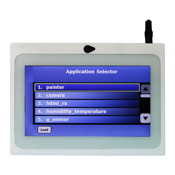
Page 106: Chapter 7 Application Selector
“Creating Your Own Loadable Applications” in section 7.4. If you have lost the contained files in the SD card, you could find them on the MAX 10 NEEK System CD under the Factory_Recovery folder. MAX 10 NEEK www.terasic.com February 4, 2016... -
Page 107: Application Selector Details
The Dual Configuration IP provides an Avalon-MM interface for NIOS II processor to access the remote system upgrade circuitry in the MAX10 FPGA device. It’s the critical part of this demonstration. The Altera Dual Configuration IP core offers the following capabilities through MAX 10 NEEK www.terasic.com February 4, 2016... -
Page 108: Running The Application Selector
The hardware design must contain a dual configuration IP in the Qsys design. (1*) IF the sof contains a Nios II processor. The hardware design must contain an Altera QSPI Flash controller as shown in Figure 7-3. MAX 10 NEEK www.terasic.com February 4, 2016... - Page 109 The configuration mode in Quartus device and options setting window should be set to dual compressed image mode as shown in Figure 7-5. Figure 7-5 Setting Configuration Mode Create your software project in Nios II Eclipse and generate the .elf file by building the MAX 10 NEEK www.terasic.com February 4, 2016...
- Page 110 Make sure the address for the QSPI flash is right and click test.bat to convert the file automatically. (3) The sof file of your design must be add to Page_1 sof data, please double check it. MAX 10 NEEK www.terasic.com February 4, 2016...
-
Page 111: Restoring The Factory Image
To convert the sof file into pof, just follow the steps for dual boot programming and make sure the sof for application selector is added to sof Page_0 data. Assuming the name of the pof is app_sel.pof. Note: (1) The original command for convert the elf into flash is: MAX 10 NEEK www.terasic.com February 4, 2016... - Page 112 Make sure the CONFIG_SEL is set to 0 and re-power up the board. Note: You can also use ‘demo_batch’ to restore the original binary file by executing the test.bat under the application_selector\demo_batch folder. MAX 10 NEEK www.terasic.com February 4, 2016...
-
Page 113: Chapter 8 Programming The Configuration Flash Memory
In dual compressed images mode, you can use the BOOT_SEL pin to select the configuration image. The High-Level Overview of Internal Configuration for MAX 10 Devices as shown in Figure 8-1. Figure 8-1 High-Level Overview of Internal Configuration for MAX 10 Devices MAX 10 NEEK www.terasic.com February 4, 2016... - Page 114 5. Reconfiguration is triggered by the following actions: Driving the nSTATUS low externally Asserting internal or external nCONFIG low Asserting RU_nCONFIG low MAX 10 NEEK www.terasic.com February 4, 2016...
-
Page 115: Using Dual Compressed Images
Save the Qsys as dual_boot.qsys and generate the HDL files. Add the dual_boot.qip into the quartus setting file and add the qsys instance in the top design file as shown in Figure 8-4. MAX 10 NEEK www.terasic.com February 4, 2016... - Page 116 The next step is to convert the two sof files into a pof file for programming the MAX10 FPGA. Open the convert programming Files tool in Quartus and set as Figure 8-6. MAX 10 NEEK www.terasic.com February 4, 2016...
- Page 117 Figure 8-8 Download the pof Now, you can set the BOOT_SEL by SW16, you will find if you set BOOT_SEL=0, the image0 will be loaded and if you set BOOT_SEL=1, he image1 will be loaded. MAX 10 NEEK www.terasic.com February 4, 2016...
-
Page 118: Nios Ii Load In Single Boot Image
In the BSP Editor (Nios II SBT for Eclipse) utility of the Eclipse, all the check box in the hal.linker table should be checked as shown in Figure 8-10. Figure 8-10 BSP Advance Setting MAX 10 NEEK www.terasic.com February 4, 2016... - Page 119 Click the Options/Boot info… button. Choose the UFM source as the load memory file and click browse button to open the onchip flash hex file as shown in 8-13. Press OK button Figure MAX 10 NEEK www.terasic.com February 4, 2016...
- Page 120 The Nios II processor can also load software from the QSPI flash on MAX 10 NEEK board. Users can refer to Application Selector demonstration for how to design the Nios II processor load software from the QSPI flash. MAX 10 NEEK www.terasic.com February 4, 2016...
-
Page 121: Chapter 9 Appendix
Chapter 9 Appendix Version Change Log V1.0 Initial Version Copyright © 2015 Terasic Inc. All rights reserved. MAX 10 NEEK www.terasic.com February 4, 2016...
Need help?
Do you have a question about the ALTERA MAX 10 NEEK and is the answer not in the manual?
Questions and answers