Table of Contents
Advertisement
Quick Links
Advertisement
Table of Contents

Related Manuals for Terasic Apollo-S10


Summary of Contents for Terasic Apollo-S10
- Page 1 Apoolo-S10 www.terasic.com 1.1. Q User Manual March 31, 2020...
-
Page 2: Table Of Contents
Setup and Status Components ............18 General User I/O ................. 22 Micro SD Card Socket ................. 24 FMC Connector ................... 25 FMC+ Connector ................. 37 Clock Circuit ..................53 USB to UART for HPS ................. 56 Apoolo-S10 www.terasic.com User Manual March 31, 2020... - Page 3 General Design Flow ................74 Using System Builder ................75 Chapter 4 Dashboard GUI ............... 84 Driver Installed on Host ............... 84 Run Dashboard GUI ................87 Chapter 5 Additional Information ............96 Getting Help ..................96 Apoolo-S10 www.terasic.com User Manual March 31, 2020...
-
Page 4: Chapter 1 Overview
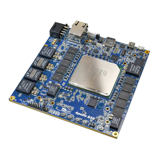
I/O planned for their systems, and build their custom systems around it. Board Layout The figures below depict the layout of the board and indicate the location of the connectors and key components. Apoolo-S10 www.terasic.com User Manual March 31, 2020... - Page 5 Figure 1-1 Apollo S10 board top Apoolo-S10 www.terasic.com User Manual March 31, 2020...
-
Page 6: Key Features
Intel Stratix ® 10 SoC FPGA : 1SX280HU2F50 2,800K logic elements (LEs) 229 Mbits embedded memory(M20K) 96 transceivers (up to 28.3Gbps) 11,520 18-bit x 19-bit multipliers 5,760 Variable-precision DSP blocks Apoolo-S10 www.terasic.com User Manual March 31, 2020... - Page 7 LED x1, Button x1, Cold Reset Button 1x6 GPIO Header Dashboard System Input Power Monitor FPGA and Board Temperature Monitorl Fan Control and Monitor Auto Fan Speed Auto Shutdown Apoolo-S10 www.terasic.com User Manual March 31, 2020...
-
Page 8: Block Diagram
Figure 1-3 Block diagram of the Apollo S10 board 1.4. Mechanical Specifications Figure 1-4 Figure 1-5 are the top and bottom Mechanical Layout of Apollo S10 board. The unit of the Mechanical Layout is millimeter (mm). Apoolo-S10 www.terasic.com User Manual March 31, 2020... - Page 9 Figure 1-4 Top side mechanical layout Figure 1-5 Bottom side mechanical layout Apoolo-S10 www.terasic.com User Manual March 31, 2020...
-
Page 10: Power Requirement
3.3V of the FMC and FMC + connector are provided by the Apollo S10 board, the carrier board does not need to provide these powers. For part number of the connector connected to J10, please refer to Table 1-1 in the section 1.6. Apoolo-S10 www.terasic.com User Manual March 31, 2020... -
Page 11: Connectivity
The Apollo S10 board provides FMC and FMC + connector as expansion interface. Users can use Apollo S10 as stand alone, connect FMC daughter card (See Figure Figure 1-8 Apollo S10 board connects to the FMC daughter card Apoolo-S10 www.terasic.com User Manual March 31, 2020... - Page 12 Users can also use Apollo-S10 as an FPGA module board and connect to other carrier boards to form a system (See Figure 1-9). Figure 1-9 Apollo S10 board connects to the based board If user wants to make their owned carrier board to connect with the Apollo S10 board,...
- Page 13 Figure 1-10 Part Number of the connector for based board Apoolo-S10 www.terasic.com User Manual March 31, 2020...
-
Page 14: Chapter 2 Board Component
Apollo S10. The peripheral circuits and usage scenarios for each mode will be listed. As shown in Figure 2-1, the mode select pin of the FPGA on the Apollo-S10 board has been set to Active Serial (AS) mode using resistors. Thus, the Apollo S10 board supports the following configuration modes: ... - Page 15 AS mode of the Apollo S10 board. Figure 2-2 AS mode for the Apollo S10 board For more information on the configuration of Stratix 10 FPGAs, please refer to the file: Intel Stratix 10 Configuration User Guide Apoolo-S10 www.terasic.com User Manual March 31, 2020...
- Page 16 Configuration firmware for the SDM FPGA I/O and HPS external memory interface (EMIF) I/O configuration data FPGA core configuration data HPS First-Stage Boot Loader(FSBL) code and FSBL hardware handoff binary data Apoolo-S10 www.terasic.com User Manual March 31, 2020...
- Page 17 Meanwhile, Terasic provides the micro SD card with built-in image data as HPS flash, which is used for HPS boot in the later part. The micro SD card stores the following data: Second-Stage Boot Loader(SSBL) Kernel Image and Device Tree Blob(DTB) ...
-
Page 18: Setup And Status Components
Illuminates when 12-V power is active. 3.3-V Power Illuminates when 3.3-V power is active. T Illuminates when the UART interface is UART_TXLED transmitting data T Illuminates when the UART interface is receiving UART_RXLED data Apoolo-S10 www.terasic.com User Manual March 31, 2020... - Page 19 FMC+ and FMC connectors will not be included in the JTAG chain if the switches are set to ON position (See Figure 2-4.).Table 2-4 lists the setting of the SW4. Figure 2-4 Position of slide switches SW4 Apoolo-S10 www.terasic.com User Manual March 31, 2020...
- Page 20 JP2 and JP3. Table 2-3 list the FMC_VCCIO Headers (JP2) setting for FMC connector. Table shows the setting of the JP3 for FMC+ connector. Figure 2-5 FMC and FMC+ I/O standard setting headers Apoolo-S10 www.terasic.com User Manual March 31, 2020...
- Page 21 Table 2-3 JP2 Setting for FMC I/O standard JP2 Setting FMC I/O Standard 1.2V 1.5V 1.8V (Default Setting) Table 2-4 JP3 Setting for FMC+ I/O standard JP3 Setting FMC I/O Standard 1.2V 1.5V 1.8V (Default Setting) Apoolo-S10 www.terasic.com User Manual March 31, 2020...
-
Page 22: General User I/O
FPGA input control. When a position of dip switch is in the DOWN position or the UPPER position, it provides a low logic level or a high logic level to the Stratix 10 SX FPGA, respectively.. Apoolo-S10 www.terasic.com User Manual March 31, 2020... - Page 23 Driving a logic 1 on the I/O port turns the LED OFF. Table 2-9 User LEDs (HPS fabric) Pin Assignments, Schematic Signal Names, and Functions Board Schematic Stratix 10 SX Description Reference Signal Name Standard Pin Number Apoolo-S10 www.terasic.com User Manual March 31, 2020...
-
Page 24: Micro Sd Card Socket
HPS SD Clock 1.8-V PIN_J30 HPS_SD_CMD HPS SD Command Line 1.8-V PIN_P30 HPS_SD_DATA[0] HPS SD Data[0] 1.8-V PIN_H30 HPS_SD_DATA[1] HPS SD Data[1] HPS_SD_DATA[2] HPS SD Data[2] 1.8-V PIN_D31 HPS_SD_DATA[3] HPS SD Data[3] 1.8-Vs PIN_H32 Apoolo-S10 www.terasic.com User Manual March 31, 2020... -
Page 25: Fmc Connector
Below we will introduce according to the individual functions of FMC connector. Figure 2-7 FMC connector on Apollo S10 board Clock Interface Table 2-11 shows the FPGA dedicated clock input pin placement on the FMC connector. Apoolo-S10 www.terasic.com User Manual March 31, 2020... - Page 26 The FPGA I/O standards of the FMC ports can be adjusted by configuring the header position. Each port can be individually adjusted to 1.2V, 1.5V or 1.8V via jumper JP2 on the Apollo S10 board. For detailed setting, please refer to Section 2.2: FMC_VCCIO Apoolo-S10 www.terasic.com User Manual March 31, 2020...
- Page 27 FMC_DP_M2C_p2/ FMC_DP_C2M_p2 , GX Channels 17.4 Gbps FMC_DP_M2C_p5/ FMC_DP_C2M_p5 , FMC_DP_M2C_p0/ FMC_DP_C2M_p0 , FMC_DP_M2C_p1/ FMC_DP_C2M_p1 , FMC_DP_M2C_p3/ FMC_DP_C2M_p3 , FMC_DP_M2C_p4/ FMC_DP_C2M_p4 GXT Channels 25 Gbps FMC_DP_M2C_p6/ FMC_DP_C2M_p6 FMC_DP_M2C_p7/ FMC_DP_C2M_p7 FMC_DP_M2C_p8/ FMC_DP_C2M_p8 FMC_DP_M2C_p9/ FMC_DP_C2M_p9 Apoolo-S10 www.terasic.com User Manual March 31, 2020...
- Page 28 FMC HA bank data p0 FMC_VCCIO *(1) FMC_HA_p[1] PIN_M12*(2) FMC HA bank data p1 FMC_VCCIO *(1) FMC_HA_p[2] PIN_D10 FMC HA bank data p2 FMC_VCCIO *(1) FMC_HA_p[3] PIN_E12 FMC HA bank data p3 FMC_VCCIO Apoolo-S10 www.terasic.com User Manual March 31, 2020...
- Page 29 FMC HA bank data n4 FMC_VCCIO *(1) FMC_HA_n[5] PIN_K11 FMC HA bank data n5 FMC_VCCIO *(1) FMC_HA_n[6] PIN_P13 FMC HA bank data n6 FMC_VCCIO *(1) FMC_HA_n[7] PIN_L14 FMC HA bank data n7 FMC_VCCIO Apoolo-S10 www.terasic.com User Manual March 31, 2020...
- Page 30 FMC HB bank data p8 FMC_VCCIO *(1) FMC_HB_p[9] PIN_AT13 FMC HB bank data p9 FMC_VCCIO *(1) FMC_HB_p[10] PIN_AM17 FMC HB bank data p10 FMC_VCCIO *(1) FMC_HB_p[11] PIN_AJ16 FMC HB bank data p11 FMC_VCCIO Apoolo-S10 www.terasic.com User Manual March 31, 2020...
- Page 31 FMC HB bank data n14 FMC_VCCIO *(1) FMC_HB_n[15] PIN_AK17 FMC HB bank data n15 FMC_VCCIO *(1) FMC_HB_n[16] PIN_AU17*(3) FMC HB bank data n16 FMC_VCCIO *(1) FMC_HB_n[17] PIN_AT18 FMC HB bank data n17 FMC_VCCIO Apoolo-S10 www.terasic.com User Manual March 31, 2020...
- Page 32 FMC LA bank data p20 FMC_VCCIO *(1) FMC_LA_p[21] PIN_C4 FMC LA bank data p21 FMC_VCCIO *(1) FMC_LA_p[22] PIN_U11 FMC LA bank data p22 FMC_VCCIO *(1) FMC_LA_p[23] PIN_V11 FMC LA bank data p23 FMC_VCCIO Apoolo-S10 www.terasic.com User Manual March 31, 2020...
- Page 33 FMC LA bank data n14 FMC_VCCIO *(1) FMC_LA_n[15] PIN_E7 FMC LA bank data n15 FMC_VCCIO *(1) FMC_LA_n[16] PIN_F5 FMC LA bank data n16 FMC_VCCIO *(1) FMC_LA_n[17] PIN_G9*(3) FMC LA bank data n17 FMC_VCCIO Apoolo-S10 www.terasic.com User Manual March 31, 2020...
- Page 34 FPGA transceiver Reference FMC_REFCLK_p PIN_T31 LVDS Clock (From on board PLL) HSSI Transmit pair p0 of the FPGA FMC_DP_C2M_p[0] PIN_M39 DIFFERENTIAL transceiver FMC_DP_C2M_p[1] PIN_L37 Transmit pair p1 of the FPGA HSSI Apoolo-S10 www.terasic.com User Manual March 31, 2020...
- Page 35 DIFFERENTIAL transceiver HSSI Receiver pair p0 of the FPGA FMC_DP_M2C_p[0] PIN_P35 DIFFERENTIAL transceiver Receiver pair p1 of the FPGA HSSI FMC_DP_M2C_p[1] PIN_R33 transceiver DIFFERENTIAL FMC_DP_M2C_p[2] PIN_M35 Receiver pair p2 of the FPGA HSSI Apoolo-S10 www.terasic.com User Manual March 31, 2020...
- Page 36 *(1): The FMC_VCCIO value depends on the setting of JP2, which can adjust the FMC_VCCIO to 1.2V, 1.5V or 1.8V. Please refer to section 2.2 : “FMC_VCCIO and FMCP_VCCIO Select Header” for details. Apoolo-S10 www.terasic.com User Manual March 31, 2020...
-
Page 37: Fmc+ Connector
Below we will introduce according to the individual functions of FMC+ connector. Compare the FMC and FMC+ Table 2-15 lists the number of I/O, power, transceiver, clock and other interfaces provided by FMC and FMC + connector on the Apollo-S10 board. Apoolo-S10 www.terasic.com User Manual March 31, 2020... - Page 38 BH37 FMCP_CLK_M2C_p1 CLK1_M2C_P CLK_2B_0P AW36 FMCP_CLK_M2C_n1 CLK1_M2C_N CLK_2B_0N AV36 FMCP_HA_p0 HA00_P_CC CLK_2A_0P BE31 FMCP_HA_n0 HA00_P_CC CLK_2A_0N BD31 FMCP_HA_p1 HA01_P_CC CLK_2A_1P AW30 FMCP_HA_n1 HA01_N_CC CLK_2A_1N AV36 FMCP_HB_p0 HB00_P_CC CLK_2F_1P AN27 FMCP_HB_n0 HB00_P_CC CLK_2F_1N AN28 Apoolo-S10 www.terasic.com User Manual March 31, 2020...
- Page 39 (SW4.1) on the Apollo S10 board. In the board's default setting, the JTAG interface of the FMC connector is bypassed to keep the Apollo S10 board JTAG chain to maintain close loop. For detailed setting, please refer to Section 2.2: JTAG Interface Apoolo-S10 www.terasic.com User Manual March 31, 2020...
- Page 40 FMC_DP_M2C_p7/ FMC_DP_C2M_p7, FMC_DP_M2C_p9/ FMC_DP_C2M_p9, FMC_DP_M2C_p10/ FMC_DP_C2M_p10 , GXT Channels FMC_DP_M2C_p12/ FMC_DP_C2M_p12 , 25 Gbps FMC_DP_M2C_p13/ FMC_DP_C2M_p13 , FMC_DP_M2C_p15/ FMC_DP_C2M_p15, FMC_DP_M2C_p16/ FMC_DP_C2M_p16, FMC_DP_M2C_p17/ FMC_DP_C2M_p17, FMC_DP_M2C_p18/ FMC_DP_C2M_p18, FMC_DP_M2C_p19/ FMC_DP_C2M_p19, FMC_DP_M2C_p20/ FMC_DP_C2M_p20 , FMC_DP_M2C_p21/ FMC_DP_C2M_p21 , Apoolo-S10 www.terasic.com User Manual March 31, 2020...
- Page 41 PIN_ AW36 FMCP_CLK_M2C_p[1] module to carrier card *(2) positive 1 *(1) Clock from mezzanine FMCP_VCCIO PIN_AV36 FMCP_CLK_M2C_n[1] module to carrier card *(2) negative 1 *(1) FMCP_HA_p[0] PIN_BE31 FMCP HA bank data p0 FMCP_VCCIO Apoolo-S10 www.terasic.com User Manual March 31, 2020...
- Page 42 FMCP HA bank data n1 FMCP_VCCIO *(1) FMCP_HA_n[2] PIN_BD30 FMCP HA bank data n2 FMCP_VCCIO *(1) FMCP_HA_n[3] PIN_AV28 FMCP HA bank data n3 FMCP_VCCIO *(1) FMCP_HA_n[4] PIN_AT30 FMCP HA bank data n4 FMCP_VCCIO Apoolo-S10 www.terasic.com User Manual March 31, 2020...
- Page 43 FMCP HB bank data p5 FMCP_VCCIO *(1) FMCP_HB_p[6] PIN_AR26 FMCP HB bank data p6 FMCP_VCCIO *(1) FMCP_HB_p[7] PIN_AT27 FMCP HB bank data p7 FMCP_VCCIO *(1) FMCP_HB_p[8] PIN_AY28 FMCP HB bank data p8 FMCP_VCCIO Apoolo-S10 www.terasic.com User Manual March 31, 2020...
- Page 44 FMCP HB bank data n11 FMCP_VCCIO *(1) FMCP_HB_n[12] PIN_BB27 FMCP HB bank data n12 FMCP_VCCIO *(1) FMCP_HB_n[13] PIN_AY26 FMCP HB bank data n13 FMCP_VCCIO *(1) FMCP_HB_n[14] PIN_BF27 FMCP HB bank data n14 FMCP_VCCIO Apoolo-S10 www.terasic.com User Manual March 31, 2020...
- Page 45 FMCP LA bank data p17 FMCP_VCCIO *(1) FMCP_LA_p[18] PIN_BE40 FMCP LA bank data p18 FMCP_VCCIO *(1) FMCP_LA_p[19] PIN_BE39 FMCP LA bank data p19 FMCP_VCCIO *(1) FMCP_LA_p[20] PIN_BF40 FMCP LA bank data p20 FMCP_VCCIO Apoolo-S10 www.terasic.com User Manual March 31, 2020...
- Page 46 FMCP LA bank data n11 FMCP_VCCIO *(1) FMCP_LA_n[12] PIN_AU37 FMCP LA bank data n12 FMCP_VCCIO *(1) FMCP_LA_n[13] PIN_AV38 FMCP LA bank data n13 FMCP_VCCIO *(1) FMCP_LA_n[14] PIN_BC38 FMCP LA bank data n14 FMCP_VCCIO Apoolo-S10 www.terasic.com User Manual March 31, 2020...
- Page 47 LVDS input from the installed FMCP card to FMCP_GBTCLK_M2C_p[1] PIN_AT41 LVDS dedicated reference clock input pin LVDS input from the FMCP_GBTCLK_M2C_p[2] PIN_AH41 installed FMCP card to LVDS dedicated reference clock Apoolo-S10 www.terasic.com User Manual March 31, 2020...
- Page 48 Transmit pair p2 of the HSSI FMCP_DP_C2M_p[2] PIN_BG47 FPGA transceiver DIFFERENTIAL Transmit pair p3 of the HSSI FMCP_DP_C2M_p[3] PIN_BE47 FPGA transceiver DIFFERENTIAL Transmit pair p4 of the HSSI FMCP_DP_C2M_p[4] PIN_BF49 FPGA transceiver DIFFERENTIAL Apoolo-S10 www.terasic.com User Manual March 31, 2020...
- Page 49 HSSI Transmit pair p13 of the FMCP_DP_C2M_p[13] PIN_AR47 DIFFERENTIAL FPGA transceiver HSSI Transmit pair p14 of the FMCP_DP_C2M_p[14] PIN_AT49 DIFFERENTIAL FPGA transceiver HSSI Transmit pair p15 of the FMCP_DP_C2M_p[15] PIN_AP49 DIFFERENTIAL FPGA transceiver Apoolo-S10 www.terasic.com User Manual March 31, 2020...
- Page 50 HSSI Receiver pair p0 of the FMCP_DP_M2C_p[0] PIN_BH41 DIFFERENTIAL FPGA transceiver Receiver pair p1 of the HSSI FMCP_DP_M2C_p[1] PIN_BJ43 FPGA transceiver DIFFERENTIAL Receiver pair p2 of the HSSI FMCP_DP_M2C_p[2] PIN_BG43 FPGA transceiver DIFFERENTIAL Apoolo-S10 www.terasic.com User Manual March 31, 2020...
- Page 51 Receiver pair p11 of the HSSI FMCP_DP_M2C_p[11] PIN_AV45 FPGA transceiver DIFFERENTIAL Receiver pair p12 of the HSSI FMCP_DP_M2C_p[12] PIN_AR43 FPGA transceiver DIFFERENTIAL Receiver pair p13 of the HSSI FMCP_DP_M2C_p[13] PIN_AT45 FPGA transceiver DIFFERENTIAL Apoolo-S10 www.terasic.com User Manual March 31, 2020...
- Page 52 Receiver pair p22 of the HSSI FMCP_DP_M2C_p[22] PIN_C43 FPGA transceiver DIFFERENTIAL HSSI Receiver pair p23 of the FMCP_DP_M2C_p[23] PIN_A43 DIFFERENTIAL FPGA transceiver Reference clock from FMCP_REFCLK_C2M_p PIN_BB35 carrier card mezzanine LVDS module to positive Apoolo-S10 www.terasic.com User Manual March 31, 2020...
-
Page 53: Clock Circuit
Clock Circuit The development board includes one 50 MHz TCXO and two programmable clock generators. Figure 2-9 shows the default frequencies of on-board all external clocks going to the Stratix 10 SX FPGA. Apoolo-S10 www.terasic.com User Manual March 31, 2020... - Page 54 Clock Switch" part in the section 2.2. Table 2-20 Clock source and clock pin to the FPGA Arria 10 Schematic Default Source GX Pin Application Signal Name Frequency Standard Number CLK_50_B2F 50.0 MHz VCCIO_FMC PIN_BA27 User Apoolo-S10 www.terasic.com User Manual March 31, 2020...
- Page 55 LVDS PIN_P9 reference clock 1 FMCP Si5341A connector FMCP_REFCLK0_p 644.53125 MHz LVDS PIN_AP41 reference clock 0 FMCP connector FMCP_REFCLK1_p 644.53125 MHz LVDS PIN_AK38 reference clock 1 FMCP FMCP_REFCLK2_p 644.53125 MHz LVDS PIN_P41 connector Apoolo-S10 www.terasic.com User Manual March 31, 2020...
-
Page 56: Usb To Uart For Hps
USB to UART for HPS The Apollo-S10 board provides a UART interface for users to communicate and transfer data with HPS through the host. This interface is mainly implemented through a USB to serial UART chip (FT232R). It can convert commands and data from the host via USB protocol to the UART interface and send it to HPS. -
Page 57: Ddr4 Sdram
Signal Name Number DDR4A_DQ0 Data [0] 1.2-V POD PIN_B35 DDR4A_DQ1 Data [1] 1.2-V POD PIN_A37 DDR4A_DQ2 Data [2] 1.2-V POD PIN_D36 DDR4A_DQ3 Data [3] 1.2-V POD PIN_B38 DDR4A_DQ4 Data [4] 1.2-V POD PIN_C35 Apoolo-S10 www.terasic.com User Manual March 31, 2020... - Page 58 1.2-V POD PIN_L25 DDR4A_DQ35 Data [35] 1.2-V POD PIN_R26 DDR4A_DQ36 Data [36] 1.2-V POD PIN_U25 DDR4A_DQ37 Data [37] 1.2-V POD PIN_P26 DDR4A_DQ38 Data [38] 1.2-V POD PIN_M25 DDR4A_DQ39 Data [39] 1.2-V POD PIN_T25 Apoolo-S10 www.terasic.com User Manual March 31, 2020...
- Page 59 PIN_T31 DDR4A_DQ69 Data [69] 1.2-V POD PIN_T34 DDR4A_DQ70 Data [70] 1.2-V POD PIN_V32 DDR4A_DQ71 Data [71] 1.2-V POD PIN_U33 DIFFERENTIAL 1.2-V PIN_A36 DDR4A_DQS0 Data Strobe p[0] DDR4A_DQS_n0 Data Strobe n[0] DIFFERENTIAL 1.2-V PIN_A35 Apoolo-S10 www.terasic.com User Manual March 31, 2020...
- Page 60 PIN_F26 DDR4A_DQS_n7 Data Strobe n[7] DIFFERENTIAL 1.2-V PIN_R32 DDR4A_DQS8 Data Strobe p[8] DIFFERENTIAL 1.2-V PIN_T32 DDR4A_DQS_n8 Data Strobe n[8] Data Bus Inversion PIN_C36 DDR4A_DBI_n0 1.2-V POD DDR4A_DBI_n1 Data Bus Inversion 1.2-V POD PIN_D39 Apoolo-S10 www.terasic.com User Manual March 31, 2020...
- Page 61 DDR4A_A11 Address [11] SSTL-12 PIN_P38 DDR4A_A12 Address [12] SSTL-12 PIN_P35 DDR4A_A13 Address [13] SSTL-12 PIN_K36 Address [14]/ SSTL-12 PIN_K37 DDR4A_A14 WE_n Address [15]/ PIN_N36 DDR4A_A15 SSTL-12 CAS_n Address [16]/ PIN_P36 DDR4A_A16 SSTL-12 RAS_n Apoolo-S10 www.terasic.com User Manual March 31, 2020...
- Page 62 DDR4 A port DDR4A_REFCLK_p LVDS PIN_M35 Reference Clock p DDR4 A port DDR4A_REFCLK_n LVDS PIN_N35 Reference Clock n External precision DDR4A_RZQ 1.2 V PIN_P34 resistor Table 2-23 DDR4B Pin Assignments, Schematic Signal Names, and Functions Apoolo-S10 www.terasic.com User Manual March 31, 2020...
- Page 63 1.2-V POD PIN_BA19 DDR4B_DQ28 Data [28] 1.2-V POD PIN_BD21 DDR4B_DQ29 Data [29] 1.2-V POD PIN_AW20 DDR4B_DQ30 Data [30] 1.2-V POD PIN_BA21 DDR4B_DQ31 Data [31] 1.2-V POD PIN_AW19 DDR4B_DQ32 Data [32] 1.2-V POD PIN_AY16 Apoolo-S10 www.terasic.com User Manual March 31, 2020...
- Page 64 1.2-V POD PIN_BF15 DDR4B_DQ63 Data [63] 1.2-V POD PIN_BD13 DDR4B_DQ64 Data [64] 1.2-V POD PIN_AP13 DDR4B_DQ65 Data [65] 1.2-V POD PIN_AR14 DDR4B_DQ66 Data [66] 1.2-V POD PIN_AP16 DDR4B_DQ67 Data [67] 1.2-V POD PIN_AU13 Apoolo-S10 www.terasic.com User Manual March 31, 2020...
- Page 65 PIN_BB14 DDR4B_DQS_n5 Data Strobe n[5] DIFFERENTIAL 1.2-V PIN_BJ15 DDR4B_DQS6 Data Strobe p[6] DIFFERENTIAL 1.2-V PIN_BH15 DDR4B_DQS_n6 Data Strobe n[6] DIFFERENTIAL 1.2-V PIN_BF16 DDR4B_DQS7 Data Strobe p[7] DIFFERENTIAL 1.2-V PIN_BE16 DDR4B_DQS_n7 Data Strobe n[7] Apoolo-S10 www.terasic.com User Manual March 31, 2020...
- Page 66 Address [6] SSTL-12 PIN_AV11 DDR4B_A7 Address [7] SSTL-12 PIN_AV12 DDR4B_A8 Address [8] SSTL-12 PIN_AW13 DDR4B_A9 Address [9] SSTL-12 PIN_AY13 DDR4B_A10 Address [10] SSTL-12 PIN_AW10 DDR4B_A11 Address [11] SSTL-12 PIN_AV10 DDR4B_A12 Address [12] SSTL-12 PIN_AN18 Apoolo-S10 www.terasic.com User Manual March 31, 2020...
- Page 67 Address Parity SSTL-12 PIN_BC11 Input Register ALERT_n DDR4B_ALERT_n 1.2 V PIN_BH18 output Activation DDR4B_ACT_n SSTL-12 PIN_BD10 Command Input DDR4B_RESET_n Chip Reset 1.2 V PIN_BF10 DDR4 B port DDR4B_REFCLK_p LVDS PIN_AT17 Reference Clock p Apoolo-S10 www.terasic.com User Manual March 31, 2020...
-
Page 68: Usb 2.0 Otg Phy
PIN_C32 HPS USB_DATA[1] HPS_USB_DATA[2] PIN_A29 HPS USB_DATA[2] 1.8V HPS_USB_DATA[3] PIN_E33 HPS USB_DATA[3] 1.8V 1.8V HPS_USB_DATA[4] PIN_F29 HPS USB_DATA[4] 1.8V HPS_USB_DATA[5] PIN_E32 HPS USB_DATA[5] 1.8V HPS_USB_DATA[6] PIN_B30 HPS USB_DATA[6] 1.8V HPS_USB_DATA[7] PIN_D29 HPS USB_DATA[7] Apoolo-S10 www.terasic.com User Manual March 31, 2020... -
Page 69: Gigabit Ethernet
Table 2-25. For instance, the connection from board to Gigabit Ethernet is established once the LEDG lights on. Table 2-25 State and Definition of LED Mode Pins LED (State) LED (Definition) Link /Activity Apoolo-S10 www.terasic.com User Manual March 31, 2020... -
Page 70: 1X6 Gpio Header
Stratix 10 FPGA (See Figure Figure 2-14). In addition to having 4 pins connected to HPS I/O, this header also provides 3.3v power and GND pin. Users can configure and use these I/O for applications through HPS. Apoolo-S10 www.terasic.com User Manual March 31, 2020... -
Page 71: System Status Interface
In addition, the board also provides USB to UART interface to connect with the System MAX, so that users can monitor the status of the board from the host through the UART interface. See chapter 8 for details. Apoolo-S10 www.terasic.com User Manual March 31, 2020... - Page 72 Figure 2-15 Block diagram of the system status interface Apoolo-S10 www.terasic.com User Manual March 31, 2020...
-
Page 73: Chapter 3 System Builder
Board damaged for wrong pin/bank voltage assignment. Board malfunction caused by wrong device connections or missing pin counts for connected ends. Performance dropped because of improper pin assignments Apoolo-S10 www.terasic.com User Manual March 31, 2020... -
Page 74: General Design Flow
I/O standard for each user-defined I/O pin. Finally, the Quartus Prime programmer must be used to download SOF file to the FPGA board using JTAG interface. Figure 3-1 the general design flow of building a project Apoolo-S10 www.terasic.com User Manual March 31, 2020... -
Page 75: Using System Builder
Figure 3-2 The System Builder window Enter Project Name The project name entered in the circled area as shown in Figure 3-4, will be assigned automatically as the name of the top-level design entry. Apoolo-S10 www.terasic.com User Manual March 31, 2020... - Page 76 The system builder can generate Verilog or VHDL Quartus top file according to the users’ requirements. Users can select their desired file type in the Top File Type list-box shown in Figure 3-5. Apoolo-S10 www.terasic.com User Manual March 31, 2020...
- Page 77 Quartus project or it would result in compilation error. Hence please do not select them if they are not needed in the design. To use the DDR4 controller, please refer to the DDR4 SDRAM demonstration in Chapter ?. Apoolo-S10 www.terasic.com User Manual March 31, 2020...
- Page 78 To use these clock, users can select the desired frequency on the Si5340A, as shown Figure 3-7. DDR4 or FMC/FMC+ must be checked before users can start to specify the desired frequency in the programmable oscillators. Apoolo-S10 www.terasic.com User Manual March 31, 2020...
- Page 79 Figure 3-8. Users can save the current board configuration information into a .cfg file and load it into the System Builder later. Apoolo-S10 www.terasic.com User Manual March 31, 2020...
- Page 80 Table 3-1 Files generated by the System Builder Filename Description <Project name>.v Top Level Verilog/VHDL File for Quartus Prime <Project name>.vhdl si5340_controller (*) Si5340A Clock Generator Controller IP <Project name>.qpf Quartus Prime Project File <Project name>.qsf Quartus Prime Setting File Apoolo-S10 www.terasic.com User Manual March 31, 2020...
- Page 81 Users can add custom logic into the project and compile the project in Quartus Prime to generate the SRAM Object File (.sof). The Si5340A controllers will be instantiated in the Quartus Prime top-level file, as listed below: Apoolo-S10 www.terasic.com User Manual March 31, 2020...
- Page 82 The following clock information also be automatically added in .sdc file. Apoolo-S10 www.terasic.com User Manual March 31, 2020...
- Page 83 If the dynamic configurations for the Si5340A clock generators are required, users need to modify the code according to users’ desired behavior. Apoolo-S10 www.terasic.com User Manual March 31, 2020...
-
Page 84: Chapter 4 Dashboard Gui
To use the dashboard system, users need to install the USB to UART driver on the host first, so that user can establish a connection with the Apollo S10 board. This section will describe how to install USB to UART driver on the windows OS host. Apoolo-S10 www.terasic.com User Manual March 31, 2020... - Page 85 Figure 4-2 Connection setup for using dashboard system Install Driver When connect the Apollo S10 board to the host PC. As shown in Figure 4-3, one USB to UART device is shown in PC Device Manager. Apoolo-S10 www.terasic.com User Manual March 31, 2020...
- Page 86 As described in previous steps, copy the device driver to the host PC and install it, as shown in Figure 4-4. Please note that the COM Port number is different in different host PC. Figure 4-4 Install USB to UART driver Apoolo-S10 www.terasic.com User Manual March 31, 2020...
-
Page 87: Run Dashboard Gui
Users can find it from the path: Tool\dashboard_gui\Dashboard.exe in the Apollo S10 system CD and copy it to the host PC. Execute the Dashboard.exe, a window will show as Figure 4-6. It will describe the detail functions as below. Apoolo-S10 www.terasic.com User Manual March 31, 2020... - Page 88 Apollo S10 board status. Users can press Stop button to stop the status data transmission and display. Reset Button: Press this button to clear the historical data shown in GUI, and record the data again. Apoolo-S10 www.terasic.com User Manual March 31, 2020...
- Page 89 “MAX_CONF_DONE” stands for FPGA configure done status. There is no LED on Apollo S10 board to display status. When this status is shown in green on the GUI, it means that FPGA configuration has been completed. Apoolo-S10 www.terasic.com User Manual March 31, 2020...
- Page 90 Apollo S10 board ambient and FPGA temperature. Users can know the board temperature in time. The information will be refreshed per 1 second, and displays through diagram and number, as shown in Figure 4-9. Apoolo-S10 www.terasic.com User Manual March 31, 2020...
- Page 91 Figure 4-9 Temperature section Fan RPM: It displays the real-time speed of the fan on the Apollo S10 board, as shown in Figure 4-10. Apoolo-S10 www.terasic.com User Manual March 31, 2020...
- Page 92 Figure 4-10 FAN RPM section 12V/Core Power monitor: It displays the real-time 12V/Core Power (0.9V) 錯誤! 找 voltage and consumption current on the Apollo S10 board, as shown in 不到參照來源。. Apoolo-S10 www.terasic.com User Manual March 31, 2020...
- Page 93 Sampling Speed: It can change interval time that the Dashboard GUI sample the board status. Users can adjust it to 1s/10s/1min/Full Speed (0.1s) to sample the board status, as shown in Figure 4-12 Figure 4-13. Apoolo-S10 www.terasic.com User Manual March 31, 2020...
- Page 94 Board Information: There is a File page on the upper left of the Dashboard GUI program window, click the Board Information to get the current software version and the Apollo S10 board version, as shown in Figure 4-14. Apoolo-S10 www.terasic.com User Manual March 31, 2020...
- Page 95 Export in the File page to save the board temperature, fan speed and voltage data in .csv format document, as shown in Figure 4-15 Figure 4-16. Figure 4-15 Export the log file Figure 4-16 Export the log file in .csv format Apoolo-S10 www.terasic.com User Manual March 31, 2020...
-
Page 96: Chapter 5 Additional Information
Here are the addresses where you can get help if you encounter problems: Terasic Technologies 9F., No.176, Sec.2, Gongdao 5 East Dist, HsinChu City, Taiwan, 30070 Email: support@terasic.com Web: www.terasic.com Apollo S10 Web: Apollo S10.terasic.com Revision History Date Version Changes 2020.03 First publication Apoolo-S10 www.terasic.com...
Need help?
Do you have a question about the Apollo-S10 and is the answer not in the manual?
Questions and answers