Table of Contents
Advertisement
Quick Links
Advertisement
Table of Contents

Related Manuals for Terasic TRDB_LCM


Summary of Contents for Terasic TRDB_LCM
- Page 1 Terasic TRDB_LCM Digital Panel Package TRDB_LCM 3.6 Inch Digital Panel Development Kit With Complete Reference Design and source code for NTSC/PAL TV Player and Pattern Generator using Altera DE2/DE1 Board TRDB_LCM Document Version 1.2 NOV. 30, 2006 by Terasic Preliminary Version...
-
Page 2: Table Of Contents
................................ 1 ONTENTS 1-2 A ..........................2 SSEMBLE THE IGITAL ANEL 1-3 G ................................ 3 ETTING CHAPTER 2 TRDB_LCM............................... 4 2-1 F ................................4 EATURES 2-2 S ............................ 5 CHEMATIC OF THE OARD 2-3 P TRDB_LCM................6 ESCRIPTION OF THE NTERFACE OF CHAPTER 3 DIGITAL PANEL DESIGN DEMONSTRATION................... -
Page 3: Chapter 1 About The Kit
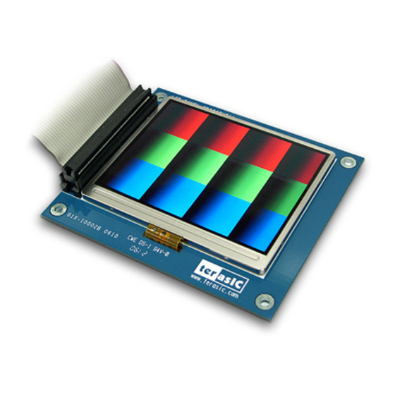
Generator using the TRDB_LCM and Altera DE2/DE1. This chapter provides users key information about the kit. Kit Contents Figure 1.1 shows the photo of the key LCD module in the TRDB_LCM package. The package includes: The TRDB_LCM board. An 40-pin IDE cable. -
Page 4: Assemble The Digital Panel
Assemble the Digital Panel Please follow the two steps below to assemble your camera: Connect the IDE cable to the back of the TRDB_LCM board, as shown in Figure 1.2. Connect the other end of the IDE cable to your DE2/DE1 board as shown in Figure 1.3. -
Page 5: Getting Help
About the Kit Getting Help Here are some places to get help if you encounter any problem: Email to support@terasic.com Taiwan & China: +886-3-550-8800 Korea : +82-2-512-7661 Japan: +81-428-77-7000 English Support Line: +1-408-512-1336... -
Page 6: Chapter 2 Trdb_Lcm
This chapter will illustrate the technical details users need to know to modify the reference design for their own purpose. Features The feature set of the TRDB_LCM is listed below: Equipped with Toppoly TD036THEA1 compact TFT LCD module. Handle digital signals of serial 8-bit (RGB or YUV). -
Page 7: Schematic Of The Board
TRDB_LCM Schematic of the Board Figure 2.1. Schematic of the TRDB_LCM... -
Page 8: Pin Description Of The 40-Pin Interface Of Trdb_Lcm
TRDB_LCM Pin Description of the 40-pin Interface of TRDB_LCM The TRDB_LCM has a 40-pin connector. The pin description of the 40-pin connector follows: Pin Numbers Name Direction Description 1~10 Not connect VCC5 Power 5V Ground 13~20 Not connect DIN6 Input... -
Page 9: Chapter 3 Digital Panel Design Demonstration
TV decoder to the cyclone II 2C35 FPGA. The FPGA on the DE2/DE1 board is handling image processing part and set the LCD module control register to display on the TRDB_LCM. Figure 3.1. The TV player Demo configuration setup... -
Page 10: Configuring The Tv Player (De2 User Only)
Digital Panel Design Demonstration Configuring the TV Player (DE2 User Only) Locate the project directory from the CD-ROM included and follow the steps below: For DE2 boards with Serial Number (S/N) starting with Digit 0 Quartus II Project Directory: DE2_LCM_TV/For_DE2_SN_0X For DE2 boards with Serial Number (S/N) starting with Digit 1 Quartus II Project Directory: DE2_LCM_TV/For_DE2_SN_1X FPGA Bitstream Used: DE2_LCM_TV.sof or DE2_LCM_TV.pof... -
Page 11: Configuring The Pattern Generator
Digital Panel Design Demonstration Configuring the Pattern Generator Locate the project directory from the CD-ROM included and follow the steps below: For DE2 User: Quartus II Project Directory: DE2_LCM_Test FPGA Bitstream Used: DE2_LCM_Test.sof or DE2_LCM_Test.pof For DE1 User: Quartus II Project Directory: DE1_LCM_Test FPGA Bitstream Used: DE1_LCM_Test.sof or DE1_LCM_Test.pof Ensure the connection is made correctly as shown in Figure 3.3. -
Page 12: Chapter 4 Appendix
Starter Kit) NOV, 30, 2006 Updated DE2_LCM_TV project for DE2 v2.0 PCB. Always Visit TRDB_LCM Webpage for New Applications We will be continuing providing interesting examples and labs on our TRDB_LCM webpage. Please visit www.altera.com or lcm.terasic.com for more information.
Need help?
Do you have a question about the TRDB_LCM and is the answer not in the manual?
Questions and answers