Table of Contents
Advertisement
Quick Links
Advertisement
Table of Contents

Related Manuals for Terasic TR10a-HL


Summary of Contents for Terasic TR10a-HL
-
Page 2: Table Of Contents
CONTENTS Chapter 1 Overview ................... 4 1.1 General Description................4 1.2 Key Features ..................5 1.3 Block Diagram ..................6 Chapter 2 Board Components ..............9 2.1 Board Overview ..................9 2.2 Configuration, Status and Setup ............10 2.3 General User Input/Output ..............13 2.4 Temperature Sensor and Fan Control .......... -
Page 4: Chapter 1 Overview
The Arria® 10 GX FPGA features integrated transceivers that transfer at a maximum of 12.5 Gbps, allowing the TR10a-HL to be fully compliant with version 3.0 of the PCI Express standard, as well as allowing an ultra low-latency, straight connections to four external 40G QSFP+ modules. -
Page 5: Key Features
Key Features The following hardware is implemented on the TR10a-HL board: FPGA Altera Arria® 10 GX FPGA (10AX115N2F45E1SG) FPGA Configuration On-Board USB Blaster II or JTAG header for FPGA programming Fast passive parallel (FPPx32) configuration via MAX II CPLD and flash memory ... -
Page 6: Block Diagram
Block Diagram Figure 1-1 shows the block diagram of the TR10a-HL board. To provide maximum flexibility for the users, all key components are connected with the Arria 10 GX FPGA device. Thus, users can configure the FPGA to implement any system design. - Page 7 1,150K logic elements (LEs) 67-Mbits embedded memory 48 transceivers (12.5Gbps) 3,036 18-bit x 19-bit multipliers 1,518 Variable-precision DSP blocks 4 PCI Express hard IP blocks 768 user I/Os 384 LVDS channels 32 phase locked loops (PLLs) ...
- Page 8 Four QSFP+ connector (40 Gbps+) PCI Express x8 edge connector Support for PCIe x8 Gen1/2/3 Edge connector for PC motherboard with x8 or x16 PCI Express slot Power Source PCI Express 6-pin DC 12V power ...
-
Page 9: Chapter 2 Board Components
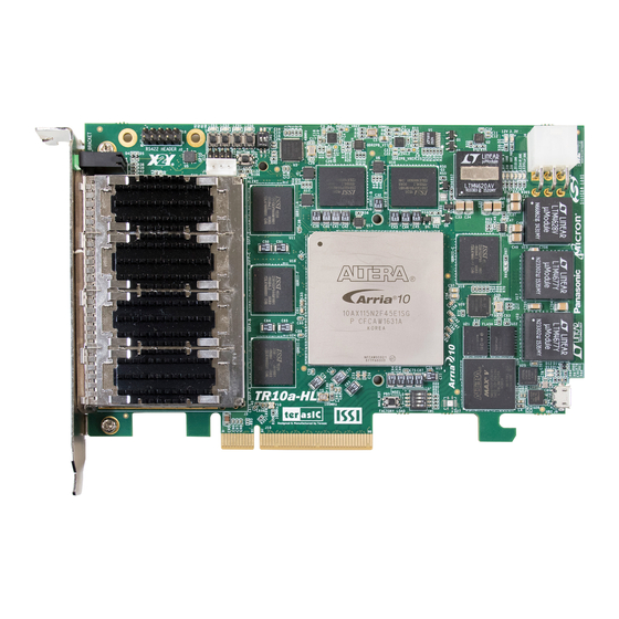
Board Overview Figure 2-1 is the top and bottom view of the TR10a-HL development board. It depicts the layout of the board and indicates the location of the connectors and key components. Users can refer to this figure for relative location of the connectors and key components. -
Page 10: Configuration, Status And Setup
Figure 2-2 FPGA Board (Bottom) Configuration, Status and Setup Configure The FPGA board supports two configuration methods for the Arria 10 FPGA: Configure the FPGA using the on-board USB-Blaster II. Flash memory configuration of the FPGA using stored images from the flash memory on power-up. - Page 11 Status LED The FPGA Board development board includes board-specific status LEDs to indicate board status. Please refer to Table 2-1 for the description of the LED indicator. Table 2-1 Status LED Board LED Name Description Reference 12-V Power Illuminates when 12-V power is active. 3.3-V Power Illuminates when 3.3-V power is active.
- Page 12 FPGA. Setting Position 4 of SW1 to “1” (down position) specifies the default factory 2-4. Setting Position 4 of SW1 to “0” (up position) image to be loaded, as shown in Figure specifies the TR10a-HL to load a user-defined image, as shown in Figure 2-5.
-
Page 13: General User Input/Output
Figure 2-4 Position of DIP switch SW1 for Image Select – Factory Image Load Figure 2-5 Position of DIP switch SW1 for Image Select – User Image Load General User Input/Output This section describes the user I/O interface to the FPGA. ... - Page 14 User-Defined Dip Switch There are two dip switches on the FPGA board to provide additional FPGA input control. When a dip switch is in the DOWN position or the UPPER position, it provides a high logic level or a low logic level to the Arria 10 GX FPGA, respectively, as shown in Figure 2-6.
-
Page 15: Temperature Sensor And Fan Control
Table 2-5 User LEDs Pin Assignments, Schematic Signal Names, and Functions Board Schematic Arria 10 GX Description Reference Signal Name Standard Pin Number LED0 LED0 1.8-V PIN_T11 LED1 LED1 1.8-V PIN_R11 LED2 LED2 1.8-V PIN_N15 Driving a logic 0 on the I/O port LED3 LED3 1.8-V... - Page 16 FPGA An optional 3-pin +12V fan located on J15 of the FPGA board is intended to reduce the temperature of the FPGA. The board is equipped with a Fan-Speed regulator and monitor, MAX6650, through an I2C interface, Users regulate and monitor the speed of fan depending on the measured system temperature.
-
Page 17: Power Monitor
Power Monitor The TR10a-HL has implemented a power monitor chip to monitor the board input power voltage and current. Figure 2-9 shows the connection between the power monitor chip and the Arria 10 GX FPGA. The power monitor chip monitors both shunt voltage drops and board input power voltage allows user to monitor the total board power consumption. -
Page 18: Clock Circuit
Clock Circuit The development board includes four 50 MHz oscillators and two programmable clock generators. Figure 2-10 shows the default frequencies of on-board all external clocks going to the Arria 10 GX FPGA. Figure 2-10 Clock circuit of the FPGA Board A clock buffer is used to duplicate the 50 MHz oscillator, so there are six 50MHz clocks fed into different five FPGA banks. - Page 19 Functions Schematic Default Arria 10 GX Source Application Signal Name Frequency Standard Pin Number CLK_50_B2H 1.8V PIN_AP34 CLK_50_B2G 1.8V PIN_AW35 CLK_50_B2F 1.8V PIN_AY31 50.0 MHz CLK_50_B3D 1.8V PIN_AN7 CLK_50_B3F 1.8V PIN_G12 CLK_50_B3H 1.8V PIN_D21 CLK_100_B3D 100.0MHz 1.8V PIN_AJ11 User-supplied OSC_100_CLKUSR 100.0MHz 1.8V PIN_AV26 configuration...
-
Page 20: Flash Memory
Table 2-9 Programmable oscillator control pin, Signal Name, I/O standard, Pin Assignments and Descriptions Programmable Schematic Arria 10 GX Description Oscillator Signal Name Standard Pin Number Si5340A Si5340A_I2C_SCL 1.8-V PIN_AU27 I2C bus, connected (U3) with Si5340A Si5340A_I2C_SDA 1.8-V PIN_AT27 Si5340A reset Si5340A_RST 1.8-V PIN_AW28... - Page 21 Figure 2-11 Connection between the Flash, Max and Arria 10 GX FPGA Table 2-10 lists the flash pin assignments, signal names, and functions. Table 2-10 Flash Memory Pin Assignments, Schematic Signal Names, and Functions Schematic Arria 10 GX Pin Description I/O Standard Signal Name Number...
- Page 22 FLASH_A17 Address bus 1.8-V PIN_F7 FLASH_A18 Address bus 1.8-V PIN_J10 FLASH_A19 Address bus 1.8-V PIN_L36 FLASH_A20 Address bus 1.8-V PIN_J18 FLASH_A21 Address bus 1.8-V PIN_H26 FLASH_A22 Address bus 1.8-V PIN_K11 FLASH_A23 Address bus 1.8-V PIN_A14 FLASH_A24 Address bus 1.8-V PIN_A15 FLASH_A25 Address bus 1.8-V...
-
Page 23: Qdrii+ Sram
FLASH_D26 Data bus 1.8-V PIN_A35 FLASH_D27 Data bus 1.8-V PIN_B33 FLASH_D28 Data bus 1.8-V PIN_AA32 FLASH_D29 Data bus 1.8-V PIN_K34 FLASH_D30 Data bus 1.8-V PIN_J35 FLASH_D31 Data bus 1.8-V PIN_B34 FLASH_CLK Clock 1.8-V PIN_T9 FLASH_RESET_n Reset 1.8-V PIN_H7 FLASH_CE_n[0] Chip enable of 1.8-V PIN_J8 offlash-0... - Page 24 QDRIIA_A1 Address bus[1] 1.8-V HSTL Class I PIN_V13 QDRIIA_A2 Address bus[2] 1.8-V HSTL Class I PIN_N10 QDRIIA_A3 Address bus[3] 1.8-V HSTL Class I PIN_M10 QDRIIA_A4 Address bus[4] 1.8-V HSTL Class I PIN_P11 QDRIIA_A5 Address bus[5] 1.8-V HSTL Class I PIN_N11 QDRIIA_A6 Address bus[6] 1.8-V HSTL Class I...
- Page 25 QDRIIA_D15 Write data bus[15] 1.8-V HSTL Class I PIN_E9 QDRIIA_D16 Write data bus[16] 1.8-V HSTL Class I PIN_E11 QDRIIA_D17 Write data bus[17] 1.8-V HSTL Class I PIN_E8 QDRIIA_Q0 Read Data bus[0] 1.8-V HSTL Class I PIN_P13 QDRIIA_Q1 Read Data bus[1] 1.8-V HSTL Class I PIN_R13 QDRIIA_Q2...
- Page 26 Functions Schematic Arria 10 GX Pin Description I/O Standard Signal Name Number QDRIIB_A0 Address bus[0] 1.8-V HSTL Class I PIN_L16 QDRIIB_A1 Address bus[1] 1.8-V HSTL Class I PIN_L15 QDRIIB_A2 Address bus[2] 1.8-V HSTL Class I PIN_E14 QDRIIB_A3 Address bus[3] 1.8-V HSTL Class I PIN_D14 QDRIIB_A4 Address bus[4]...
- Page 27 QDRIIB_D11 Write data bus[11] 1.8-V HSTL Class I PIN_D19 QDRIIB_D12 Write data bus[12] 1.8-V HSTL Class I PIN_E19 QDRIIB_D13 Write data bus[13] 1.8-V HSTL Class I PIN_C18 QDRIIB_D14 Write data bus[14] 1.8-V HSTL Class I PIN_G19 QDRIIB_D15 Write data bus[15] 1.8-V HSTL Class I PIN_K19 QDRIIB_D16...
- Page 28 On-Die Termination QDRIIB_ODT 1.8-V HSTL Class I PIN_M17 Input Valid Output QDRIIB_QVLD 1.8-V HSTL Class I PIN_G22 Indicator Table 2-13 QDRII+ SRAM C Pin Assignments, Schematic Signal Names, and Functions Schematic Arria 10 GX Pin Description I/O Standard Signal Name Number QDRIIC_A0 Address bus[0]...
- Page 29 QDRIIC_D5 Write data bus[5] 1.8-V HSTL Class I PIN_AB34 QDRIIC_D6 Write data bus[6] 1.8-V HSTL Class I PIN_AA35 QDRIIC_D7 Write data bus[7] 1.8-V HSTL Class I PIN_AA34 QDRIIC_D8 Write data bus[8] 1.8-V HSTL Class I PIN_Y34 QDRIIC_D9 Write data bus[9] 1.8-V HSTL Class I PIN_AF32 QDRIIC_D10...
- Page 30 Class I QDRIIC_CQ_p 1.8-V HSTL Class I PIN_AD36 Echo clock P QDRIIC_CQ_n 1.8-V HSTL Class I PIN_AC36 Echo clock N QDRIIC_RPS_n 1.8-V HSTL Class I PIN_E26 Report Select QDRIIC_WPS_n 1.8-V HSTL Class I PIN_F26 Write Port Select QDRIIC_DOFF_n 1.8-V HSTL Class I PIN_D24 PLL Turn Off On-Die Termination...
- Page 31 QDRIID_A21 Address bus[21] 1.8-V HSTL Class I PIN_L35 QDRIID_D0 Write data bus[0] 1.8-V HSTL Class I PIN_D36 QDRIID_D1 Write data bus[1] 1.8-V HSTL Class I PIN_F34 QDRIID_D2 Write data bus[2] 1.8-V HSTL Class I PIN_D34 QDRIID_D3 Write data bus[3] 1.8-V HSTL Class I PIN_D35 QDRIID_D4 Write data bus[4]...
- Page 32 QDRIID_Q17 Read Data bus[17] 1.8-V HSTL Class I PIN_P28 QDRIID_BWS_n0 1.8-V HSTL Class I PIN_C37 Byte Write select[0] QDRIID_BWS_n1 1.8-V HSTL Class I PIN_F37 Byte Write select[1] Differential 1.8-V QDRIID_K_p PIN_F32 Clock P HSTL Class I Differential 1.8-V QDRIID_K_n Clock N PIN_E32 HSTL Class I QDRIID_CQ_p...
- Page 33 QDRIIE_A17 Address bus[17] 1.8-V HSTL Class I PIN_AL14 QDRIIE_A18 Address bus[18] 1.8-V HSTL Class I PIN_AM14 QDRIIE_A19 Address bus[19] 1.8-V HSTL Class I PIN_AT14 QDRIIE_A20 Address bus[20] 1.8-V HSTL Class I PIN_AU14 QDRIIE_A21 Address bus[21] 1.8-V HSTL Class I PIN_AP13 QDRIIE_D0 Write data bus[0] 1.8-V HSTL Class I...
- Page 34 QDRIIE_Q13 Read Data bus[13] 1.8-V HSTL Class I PIN_AV15 QDRIIE_Q14 Read Data bus[14] 1.8-V HSTL Class I PIN_BA15 QDRIIE_Q15 Read Data bus[15] 1.8-V HSTL Class I PIN_AW16 QDRIIE_Q16 Read Data bus[16] 1.8-V HSTL Class I PIN_AY16 QDRIIE_Q17 Read Data bus[17] 1.8-V HSTL Class I PIN_AY17 QDRIIE_BWS_n0...
- Page 35 QDRIIF_A13 Address bus[13] 1.8-V HSTL Class I PIN_AL12 QDRIIF_A14 Address bus[14] 1.8-V HSTL Class I PIN_AT9 QDRIIF_A15 Address bus[15] 1.8-V HSTL Class I PIN_AV7 QDRIIF_A16 Address bus[16] 1.8-V HSTL Class I PIN_AV6 QDRIIF_A17 Address bus[17] 1.8-V HSTL Class I PIN_AU9 QDRIIF_A18 Address bus[18] 1.8-V HSTL Class I...
-
Page 36: Qspf+ Ports
QDRIIF_Q9 Read Data bus[9] 1.8-V HSTL Class I PIN_W11 QDRIIF_Q10 Read Data bus[10] 1.8-V HSTL Class I PIN_V10 QDRIIF_Q11 Read Data bus[11] 1.8-V HSTL Class I PIN_W10 QDRIIF_Q12 Read Data bus[12] 1.8-V HSTL Class I PIN_W9 QDRIIF_Q13 Read Data bus[13] 1.8-V HSTL Class I PIN_Y13 QDRIIF_Q14... - Page 37 Figure 2-12 Connection between the QSFP+ and Arria GX FPGA Table 2-17, Table 2-18, Table 2-19 Table 2-20 list the QSFP+ A, B, C and D pin assignments and signal names relative to the Arria 10 GX device. Table 2-17 QSFP+ A Pin Assignments, Schematic Signal Names, and Functions Schematic Arria 10 GX Description...
- Page 38 QSFPA_MOD_SEL_n Module Select 1.8V PIN_AC10 QSFPA_RST_n Module Reset 1.8V PIN_AA9 QSFPA_SCL 2-wire serial interface clock 1.8V PIN_AA10 QSFPA_SDA 2-wire serial interface data 1.8V PIN_Y9 QSFPA_LP_MODE Low Power Mode 1.8V PIN_AB10 QSFPA_INTERRUPT_n Interrupt 1.8V PIN_AB9 QSFPA_MOD_PRS_n Module Present 1.8V PIN_AG10 Table 2-18 QSFP+ B Pin Assignments, Schematic Signal Names, and Functions Schematic Arria 10 GX Description...
- Page 39 Table 2-19 QSFP+ C Pin Assignments, Schematic Signal Names, and Functions Arria 10 Schematic Description I/O Standard GX Pin Signal Name Number QSFPC_TX_P0 Transmitter data of channel 0 1.4-V PCML PIN_AB1 QSFPC_TX_N0 Transmitter data of channel 0 1.4-V PCML PIN_AB2 QSFPC_RX_P0 Receiver data of channel 0 1.4-V PCML...
-
Page 40: Pci Express
QSFPD_TX_P1 Transmitter data of channel 1 1.4-V PCML PIN_H1 QSFPD_TX_N1 Transmitter data of channel 1 1.4-V PCML PIN_H2 QSFPD_RX_P1 Receiver data of channel 1 1.4-V PCML PIN_G3 QSFPD_RX_N1 Receiver data of channel 1 1.4-V PCML PIN_G4 QSFPD_TX_P2 Transmitter data of channel 2 1.4-V PCML PIN_F1 QSFPD_TX_N2... - Page 41 to 6-pin 12V DC power connector in the FPGA to avoid FPGA damage due to insufficient power. The PCIE_REFCLK_p signal is a differential input that is driven from the PC motherboard on this board through the PCIe edge connector. A DIP switch (SW2) is connected to the PCI Express to allow different configurations to enable a x1, x4, or x8 PCIe.
- Page 42 PCIE_TX_n5 Add-in card transmit bus 1.4-V PCML PIN_AH43 PCIE_TX_p6 Add-in card transmit bus 1.4-V PCML PIN_AF44 PCIE_TX_n6 Add-in card transmit bus 1.4-V PCML PIN_AF43 PCIE_TX_p7 Add-in card transmit bus 1.4-V PCML PIN_AD44 PCIE_TX_n7 Add-in card transmit bus 1.4-V PCML PIN_AD43 PCIE_RX_p0 Add-in card receive bus 1.4-V PCML...
-
Page 43: Qspf+ Ports
2.11 QSPF+ Ports The 2x5 RS-422 expansion header is designed to perform communication between boards. Users can use Terasic defined RS422-RJ45 board to translate RS-422 signal, allowing a transmission speed of up to 26 Mbps. Figure 2-14 shows the RS-422 application diagram. - Page 44 between 2x4 GPIO header and Arria 10 GX FPGA. Table 2-23 lists the pin assignment of 2x4 GPIO header. Figure 2-15 Connection between 2x4 GPIO Header and Arria 10 GX FPGA Table 2-23 Pin Assignments of 2x4 GPIO Header Schematic Arria 10 GX Description I/O Standard...
-
Page 45: Chapter 3 System Builder
Chapter 3 System Builder his chapter describes how users can create a custom design project for the FPGA board from a software tool named System Builder. Introduction The System Builder is a Windows based software utility. It is designed to help users create a Quartus II project for the FPGA board within minutes. -
Page 46: General Design Flow
General Design Flow This section provides the detail procedures on how the System Build This section will introduce the general design flow to build a project for the FPGA board via the System Builder. The general design flow is illustrated in the Figure 3-1. -
Page 47: Using System Builder
Using System Builder This section provides the detail procedures on how the System Builder is used. Install and Launch the System Builder The System Builder is located under the directory: "Tools\SystemBuilder" in the System CD. Users can copy the entire folder to the host computer without installing the utility. - Page 48 Figure 3-3 The Quartus project name System Configuration Users are given the flexibility of enabling their choices of components connected to the FPGA under System Configuration, as shown in Figure 3-4. Each component of the FPGA board is listed to be enabled or disabled according to users’ needs. If a component is enabled, the System Builder will automatically generate the associated pin assignments including its pin name, pin location, pin direction, and I/O standards.
- Page 49 Figure 3-4 System Configuration group Programmable Oscillator There are two external oscillators on-board that provide reference clocks for the following signals QSFPA_REFCLK,QSFPB_REFCLK,QSFPC_REFCLK,QSFPD_REFCLK, QDRIIA_REFCLK, QDRIIB_REFCLK, QDRIIC_REFCLK , QDRIID_REFCLK , QDRIIE_REFCLK and QDRIIF_REFCLK. To use these clock, users can select the desired frequency on the Programmable Oscillator group, as shown in Figure 3-5.
- Page 50 Figure 3-5 External programmable oscillators Project Setting Management The System Builder also provides functions to restore default setting, load a setting, and save board configuration file, as shown in Figure 3-6. Users can save the current board configuration information into a .cfg file and load it into the System Builder. Figure 3-6 Project Settings...
- Page 51 Project Generation When users press the Generate button, the System Builder will generate the corresponding Quartus II files and documents as listed in theTable 3-1 in the directory specified by the user. Table 3-1 Files generated by the System Builder Filename Description <Project name>.v...
- Page 52 For Si5340B, its controller will be instantiated in the Quartus II top-level file, as listed below: If the dynamic configuration for the oscillator is required, users need to modify the code according to users’ desired behavior.
-
Page 53: Flash Programming
Chapter 4 Flash Programming s you develop your own project using the Altera tools, you can program the flash memory device so that your own design loads from flash memory into the FPGA on power up. This chapter will describe how to use Altera Quartus II Programmer Tool to program the common flash interface (CFI) flash memory device on the FPGA board. -
Page 54: Fpga Configure Operation
tool elf2flash can be used. For convenience, the System CD contains a batch file for file translation and flash programming with users given .sof and .elf file. FPGA Configure Operation Here is the procedure to enable FPGA configuration from Flash: Please make sure the FPGA configuration data has been stored in the CFI flash. -
Page 55: Flash Programming With Users Design
Flash Programming with Users Design Users can program the flash memory device so that a custom design loads from flash memory into the FPGA on power up. For convenience, the translation and programming batch files are available on the following folder in the System CD. Demonstrations/Hello/flash_programming_batch There folder contains five files as shown in Table 4-2... -
Page 56: Restore Factory Settings
If your design includes a NIOS II processor and the NIOS II program is stored on external memory, users must to perform following items so the NIOS II program can be boot from flash successfully: 1. QSYS should include a Flash controller for the CFI Flash on the development board. - Page 57 Make sure the Nios II EDS and USB-Blaster II driver are installed. Make sure the FPGA board and PC are connected with an UBS Cable. Power on the FPGA board. Copy the “Demonstrations/PFL/flash_programming_batch” folder under the CD to your PC’s local drive. Execute the batch file flash_program.bat to start flash programming.
-
Page 58: Peripheral Reference Design
Si5340 to output desired frequencies, as well as how to control the fan speed. The source codes and tool of these examples are all available on the System Configure Si5340A/B in RTL There are two Silicon Labs Si5340 clock generators on TR10a-HL FPGA board can provide adjustable frequency reference clock (See Figure 5-1) for QSFP and QDRII interfaces, etc. - Page 59 Creating Si5340 Control IP The Si5340 control IP is located in the folder: \Demonstration\si5340_control_ip”. Also, System Builder tool ( locate in System CD) can be used to help users to set Si5340 to output desired frequencies, and generate a Quartus project with control IP. In System Builder window, when checking the boxes of QSFP and QDRII interfaces, Si5340 corresponding output channels will become available and users can select desired frequencies.
- Page 60 Figure 5-3 Enable Si5340A and Si5340B clock on System Builder Click "Generate" button, then, open the Quartus Project generated by System Builder, the control IPs for Si5340A and Si5340B can be found in the top level file. //======================================================= // Configure SI5340A //======================================================= `define SI5340A_POWER_DOWN 3'h0 `define SI5340A_644M53125...
- Page 61 .iRST_n(CPU_RESET_n), .iStart(si5340a_controller_start), .iPLL_OUT0_FREQ_SEL(`SI5340A_644M53125),//QSFP-A .iPLL_OUT1_FREQ_SEL(`SI5340A_644M53125),//QSFP-B .iPLL_OUT2_FREQ_SEL(`SI5340A_644M53125),//QSFP-C .iPLL_OUT3_FREQ_SEL(`SI5340A_644M53125),//QSFP-D .I2C_CLK(SI5340A_I2C_SCL), .I2C_DATA(SI5340A_I2C_SDA), .oPLL_REG_CONFIG_DONE(si5340a_config_done) assign SI5340A_OE_n = 1'b0; assign SI5340A_RST_n = CPU_RESET_n; //======================================================= // Configure SI5340B //======================================================= `define REFCLK_QDR275 4'h0 `define REFCLK_QDR250 4'h1 `define REFCLK_QDR225 4'h2 wire si5340b_controller_start; wire si5340b_config_done; assign si5340b_controller_start = ~BUTTON[0]; si5340b_controller si5340b_controller( .iCLK(CLK_50_B2F), .iRST_n(CPU_RESET_n), .iStart(si5340b_controller_start),...
- Page 62 assign SI5340B_RST_n = CPU_RESET_n; If the output frequency doesn’t need to be modified, users can just add their own User Logic and compile it, and then, Si5340 can output desired frequencies. At the same time, System Builder will set Clock constrain according user’s preset frequency in a SDC file (as shown in Figure 5-4).
- Page 63 Configuration in Progress, 1: Configuration Complete) I2C_DATA inout I2C Serial Data to/fromSi5340 I2C_CLK output I2C Serial Clock to Si5340 As shown in Table 5-2and Table 5-3, both two Si5340 control IPs have preset several output frequency parameters, if users want to change frequency, users can fill in the input port "...
- Page 64 Users can also dynamically modify the input parameters, and input a positive edge trigger for “iStart”, then, Si5340 output frequency can be modified. After the manually modifying, please remember to modify the corresponding frequency value in SDC file. Modify Clock Parameter For Your Own Frequency If the Si5340 control IP build-in frequencies are not users’...
- Page 65 After the installation, select Si5340, and configure the input frequency and output frequency as shown in Figure 5-6. Figure 5-6 Define Output Clock Frequencies on ClockBuilder Pro Wizard After the setting is completed, ClockBuider Pro Wizard generates a Design Report(text), which contains users setting frequency corresponding register value (See Figure 5-7).
- Page 66 Figure 5-7 Open Design Report on ClockBuilder Pro Wizard Open Si5340 control IP sub-module “si5340a_i2c_reg_controller.v “ as shown inFigure5-8, refer Design Report parameter modify sub-module corresponding register value (See Figure 5-9). Figure 5-8 Sub-Module file "si5340a_i2c_reg_controller.v" Figure 5-9 Modify Si5340 Control IP Base on Design Report After modifying and compiling, Si5340 can output new frequencies according to the users’...
-
Page 67: Nios Ii Control For Si5340/Temperature/Power
2. After the manually modifying, please remember to modify clock constrain setting in .SDC file Nios II control for SI5340/Temperature/Power This demonstration shows how to use the Nios II processor to program two programmable oscillators (Si5340A and Si5340B) on the FPGA board, how to measure the power consumption based on the built-in power measure circuit. - Page 68 Figure 5-10 Block diagram of the Nios II Basic Demonstration The program provides a menu in nios-terminal, as shown in Figure 5-11 to provide an interactive interface. With the menu, users can perform the test for the temperatures sensor, external PLL and power monitor. Note, pressing ‘ENTER’ should be followed with the choice number.
- Page 69 TR10a-HL board, there will be a voltage drop (named ∆SENSE Voltage) on R96. Based on sense resistors, the program of power monitor can calculate the associated voltage, current and power consumption from the LTC2945 through the I2C interface.
- Page 70 For programmable PLL Si5340A test, please input key ‘2’ and press ‘Enter’ in the nios-terminal first, then select the desired output frequency of QSFPA/B/C/D REFCLK, as shown in Figure 5-14. For programmable PLL Si5340B test, please input key ‘3’ and press ‘Enter’ in the nios-terminal first, then select the desired output frequency of QDRIIA/B/C/D/E/F REFCLK, as shown in Figure...
- Page 71 Figure 5-14 Si5340A Demo Figure 5-15 Si5340B Demo...
-
Page 72: Fan Speed Control
Fan Speed Control This demo helps users quickly understand how to set the MAX6650 chip from the FPGA to control the fansink. The MAX6650 chip can set or retrieve the RPM of the fansink. It can also monitor if there is any unexpected error and determine which type of error it is. The following section will save lots of time for the development of user application. - Page 73 Figure 5-16 Block diagram of the fan speed control demonstration Alarm Status Register Bit Assignments When the fan is abnormal, the LED will lit. Users can refer to Table 5-4 and get a better understanding about the malfunction of the fansink accordingly. The status of BIT 4 ~ 7 can be ignored because BIT 4 is for MAX6651 only and BIT 5 ~ 7 are always low.
- Page 74 FPGA Configure File: TR10A_HL_golden_top.sof Demonstration Setup Make sure Quartus II is installed on the host PC. Connect the TR10a-HL and the host PC via USB cable. Install the USB-Blaster II driver if necessary. Power on the FPGA Board. ...
-
Page 75: Memory Reference Design
Chapter 6 Memory Reference Design his chapter will show two examples which use the Altera Memory IP to perform memory test functions. The source codes of these examples are all available on the FPGA System CD. These three examples are: ... - Page 76 Figure 6-1 shows the function block diagram of the demonstration. The six QDRII+ SRAM controllers are configured as a 72Mb controller. The QDRII+ SRAM IP generates a 550MHz clock as memory clock and a half-rate system clock, 275MHz, for the controllers.
- Page 77 Figure 6-1 Function Block Diagram of the QDRII+ SRAM x4 Demonstration The QDRIIA/B/C/D_REFCLK is generated from Si5340B which configured 275MHz for QDRII+ 550MHz by Clock Config module. QDRIIA/B/C/D_REFCLK has no default frequency output so that they must be configured first. In this demonstration, each QDRII+ SRAM has its own PLL, DLL and OCT resources.
- Page 78 read back data with the regenerated data (the same sequence as the write data). Test control signals for four QDRII+ SRAMs will generate from CPU_RESET_n and four LEDs will indicate the test results of four QDRII+ SRAMs. Altera QDRII and QDRII+ SRAM Controller with UniPHY To use Altera QDRII+ SRAM controller, users need to perform the following steps in order: 1.
-
Page 79: Qdrii+ Sram Test By Nios Ii
Table 6-1 LED Indicators NAME Description LED0 QDRII+ SRAM(A) test result LED1 QDRII+ SRAM(B) test result LED2 QDRII+ SRAM(C) test result LED3 QDRII+ SRAM(D) test result Bracket LED0 QDRII+ SRAM(E) test result Bracket LED1 QDRII+ SRAM(F) test result QDRII+ SRAM Test by Nios II This demonstration hardware and software designs are provided to illustrate how to perform QDRII+ SRAM memory access in QSYS. - Page 80 Figure 6-2 Block diagram of the QDRII+ Demonstration The system flow is controlled by a Nios II program. First, the Nios II program writes test patterns into the whole 8 MB of SRAM. Then, it calls Nios II system function, alt_dcache_flush_all(), to make sure all data has been written to SRAM.
- Page 81 Demonstration Batch File Demo Batch File Folder: NIOS_QDRII_x6_550\demo_batch The demo batch file includes following files: Batch File for USB-Blaseter II: test.bat, test.sh FPGA Configure File: NIOS_QDRII_x6_550.sof Nios II Program: TEST_QDRII.elf Demonstration Setup Please follow below procedures to setup the demonstartons. ...
- Page 82 Figure 6-3 Progress and Result Information for the QDRII+ Demonstration...
-
Page 83: Pci Express Reference Design
It consists of two primary components: FPGA System and PC System. The FPGA System is developed based on Arria 10 Hard IP for PCI Express with Avalon-MM DMA. The application software on the PC side is developed by Terasic based on Altera’s PCIe kernel mode driver. -
Page 84: Pc Pci Express Software Sdk
Figure 7-1 Infrastructure of PCI Express System PC PCI Express Software SDK The FPGA System CD contains a PC Windows based SDK to allow users to develop their 64-bit software application on Windows 7/Window XP 64-bit. The SDK is located in the "CDROM \demonstrations\PCIe_SW_KIT"... -
Page 85: Pci Express Software Stack
communicate with the FPGA. The library provides the following functions: Basic data read and write Data read and write by DMA For high performance data transmission, Altera AVMM DMA is required as the read and write operations are specified under the hardware design on the FPGA. PCI Express Software Stack Figure 7-2 shows the software stack for the PCI Express application software on 64-bit... - Page 86 WdfCoinstaller01011.dll To install the PCI Express driver, please execute the steps below: 1. Install the TR10a-HL on the PCIe slot of the host PC 2. Make sure Altera Programmer and USB-Blaster II driver are installed 3. Execute test.bat in "CDROM\Demonstrations\PCIe_Fundamental\demo_batch"...
- Page 87 6. In the How do you want to search for driver software dialog, click Browse my computer for driver software item, as shown in Figure 7-4 Figure 7-4 Dialog of Browse my computer for driver software 7. In the Browse for driver software on your computer dialog, click the Browse button to specify the folder where altera_pcie_din_driver.inf is located, as shown Figure 7-5.
- Page 88 8. When the Windows Security dialog appears, as shown Figure 7-6, click the Install button. Figure 7-6 Click Install in the dialog of Windows Security 9. When the driver is installed successfully, the successfully dialog will appears, as shown in Figure 7-7.
- Page 89 Once the driver is successfully installed, users can see the Altera PCI API Driver under the device manager window, as shown in Figure7-8. Figure 7-8 Altera PCI API Driver in Device Manager Create a Software Application All the files needed to create a PCIe software application are located in the directory CDROM\demonstration\PCIe_SW_KIT\PCIe_Library.
- Page 90 Function: Open a specified PCIe card with vendor ID, device ID, and matched card index. Prototype: PCIE_HANDLE PCIE_Open( WORD wVendorID, WORD wDeviceID, WORD wCardIndex); Parameters: wVendorID: Specify the desired vendor ID. A zero value means to ignore the vendor ID. wDeviceID: Specify the desired device ID.
- Page 91 bool PCIE_Read32( PCIE_HANDLE hPCIE, PCIE_BAR PcieBar, PCIE_ADDRESS PcieAddress, DWORD * pdwData); Parameters: hPCIE: A PCIe handle return by PCIE_Open function. PcieBar: Specify the target BAR. PcieAddress: Specify the target address in FPGA. pdwData: A buffer to retrieve the 32-bit data. Return Value: Return TRUE if read data is successful;...
- Page 92 PCIE_DmaRead Function: Read data from the memory-mapped memory of FPGA board in DMA. Maximal read size is (4GB-1) bytes. Prototype: bool PCIE_DmaRead( PCIE_HANDLE hPCIE, PCIE_LOCAL_ADDRESS LocalAddress, void *pBuffer, DWORD dwBufSize Parameters: hPCIE: A PCIe handle return by PCIE_Open function. LocalAddress: Specify the target memory-mapped address in FPGA.
-
Page 93: Pcie Reference Design - Fundamental
Parameters: hPCIE: A PCIe handle return by PCIE_Open function. LocalAddress: Specify the target memory mapped address in FPGA. pData: A pointer to a memory buffer to store the data which will be written to FPGA. dwDataSize: Specify the byte number of data which will be written to FPGA. Return Value: Return TRUE if write data is successful;... - Page 94 Demonstration Files Location The demo file is located in the batch folder: CDROM\demonstrations\PCIe_funcdamental\demo_batch The folder includes following files: FPGA Configuration File: PCIe_Fundamental.sof Download Batch file: test.bat Windows Application Software folder : windows_app, includes PCIE_FUNDAMENTAL.exe TERASIC_PCIE_AVMM.dll ...
- Page 95 Figure 7-10 Screenshot for PCIe Driver 6. Goto windows_app folder, execute PCIE_FUNDMENTAL.exe. A menu will appear as shown in Figure 7-11. Figure 7-11 Screenshot of Program Menu 7. Type 0 followed by a ENTERY key to select Led Control item, then input 15 (hex 0x0f) will make all led on as shown in Figure 7-12.
- Page 96 Figure 7-12 Screenshot of LED Control 8. Type 1 followed by an ENTERY key to select Button Status Read item. The button status will be report as shown in Figure 7-13. Figure 7-13 Screenshot of Button Status Report 9. Type 2 followed by an ENTERY key to select DMA Testing item. The DMA test result will be report as shown in Figure 7-14.
- Page 97 Figure 7-14 Screenshot of DMA Memory Test Result 10. Type 99 followed by an ENTERY key to exit this test program Development Tools Quartus II 16.0 Visual C++ 2012 Demonstration Source Code Location Quartus Project: Demonstrations\PCIe_Fundamental ...
- Page 98 Figure 7-15 Hardware block diagram of the PCIe reference design Windows Based Application Software Design The application software project is built by Visual C++ 2012. The project includes the following major files: Name Description PCIE_FUNDAMENTAL.cpp Main program PCIE.c Implement dynamically load for TERAISC_PCIE_AVMM.DLL PCIE.h TERASIC_PCIE_AVMM.h...
- Page 99 The base address of BUTTON and LED controllers are 0x4000010 and 0x4000020 based on PCIE_BAR4, in respectively. The on-chip memory base address is 0x00000000 relative to the DMA controller. Before accessing the FPGA through PCI Express, the application first calls PCIE_Load to dynamically load the TERASIC_PCIE_AVMM.DLL.
-
Page 100: Pcie Reference Design - Qdrii
PCIe Reference Design – QDRII+ The application reference design shows how to add QDRII+ Memory Controllers for six QDRII+ SRAMs into the PCIe Quartus project based on the PCI_Fundamental Quartus project and perform 8MB data DMA for six SRAMs. Also, this demo shows how to call "PCIE_ConfigRead32"... - Page 101 7. Type 2 followed by a ENTERY key to select Link Info item. The PICe link information will be shown as in Figure 7-17. Gen3 link speed and x8 link width are expected. Figure 7-17 Screenshot of Link Info 8. Type 3 followed by an ENTERY key to select DMA On-Chip Memory Test item. The DMA write and read test result will be report as shown in Figure 7-18.
- Page 102 9. Type 4 followed by an ENTERY key to select DMA QDRII-A Memory Test item. The DMA write and read test result will be report as shown in Figure 7-19. Figure 7-19 Screenshot of QDRII-A Memory DAM Test Result 10. Type 5 followed by an ENTERY key to select DMA QDRII-B Memory Test item. The DMA write and read test result will be report as shown in Figure 7-20.
- Page 103 Figure 7-21 Screenshot of QDRII-C Memory DAM Test Result 12. Type 7 followed by an ENTERY key to select DMA QDRII-D Memory Test item. The DMA write and read test result will be report as shown in Figure 7-22. Figure 7-22 Screenshot of QDRII-D Memory DAM Test Result 13.
- Page 104 14. Type 9 followed by an ENTERY key to select DMA QDRII-A Memory Test item. The DMA write and read test result will be report as shown in Figure 7-24. Figure 7-24 Screenshot of QDRII-F Memory DAM Test Result 15. Type 99 followed by an ENTERY key to exit this test program. ...
- Page 105 Figure 7-25 Hardware block diagram of the PCIe QDRII+ reference design Windows Based Application Software Design The application software project is built by Visual C++ 2012. The project includes the following major files: Name Description PCIE_QDR.cpp Main program PCIE.c Implement dynamically load for TERAISC_PCIE_AVMM.DLL PCIE.h...
- Page 106 The base address of BUTTON and LED controllers are 0x4000010 and 0x4000020 based on PCIE_BAR4, in respectively. The on-chip memory base address is 0x00000000 relative to the DMA controller. The above definition is the same as those in PCIe Fundamental demo. Before accessing the FPGA through PCI Express, the application first calls PCIE_Load to dynamically load the TERASIC_PCIE_AVMM.DLL.
-
Page 108: Chapter 8 Transceiver Verification
Transceiver Verification his chapter describes how to verify the FPGA transceivers for the QSFP+ by using the test code provided in the TR10a-HL system CD. Function of the Transceiver Test Code The transceiver test code is used to verify the transceiver channels for the QSPF+ ports through an external loopback method. - Page 109 Figure 8-1 Optical QSFP+ Cable Figure 8-2QSFP+ Loopback Fixture Figure 8-3 shows the FPGA board with two QSFP+ cable installed. Figure 8-4 shows the FPGA board with four QSFP+ loopback fixtures installed. Figure 8-3 Two QSFP+ Cables Installed...
-
Page 110: Testing
Figure 8-4 Four QSFP+ Loopback Fixtures Installed Testing The transceiver test code is available in the folder System CD\Tool\Transceiver_Test. Here are the procedures to perform transceiver channel test: Copy Transceiver_Test folder to your local disk. Ensure that the FPGA board is NOT powered on. Plug-in the QSPF+ loopback fixtures. - Page 111 Figure 8-5QSFP+ Transceiver Loopback Test in Progress Figure 8-6QSFP Transceiver Loopback Done...
-
Page 112: Chapter 9 Additional Information
Here are the addresses where you can get help if you encounter problems: Terasic Technologies 9F., No.176, Sec.2, Gongdao 5th Rd, East Dist, HsinChu City, Taiwan, 30070 Email: support@terasic.com Web: www.terasic.com TE10a-HL Web: tr10a-hl.terasic.com Revision History Date Version Changes 2016.11...
Need help?
Do you have a question about the TR10a-HL and is the answer not in the manual?
Questions and answers