Table of Contents
Advertisement
Quick Links
Chipsmall Limited consists of a professional team with an average of over 10 year of expertise in the distribution
of electronic components. Based in Hongkong, we have already established firm and mutual-benefit business
relationships with customers from,Europe,America and south Asia,supplying obsolete and hard-to-find components
to meet their specific needs.
With the principle of "Quality Parts,Customers Priority,Honest Operation,and Considerate Service",our business
mainly focus on the distribution of electronic components. Line cards we deal with include
Microchip,ALPS,ROHM,Xilinx,Pulse,ON,Everlight and Freescale. Main products comprise
IC,Modules,Potentiometer,IC Socket,Relay,Connector.Our parts cover such applications as commercial,industrial,
and automotives areas.
We are looking forward to setting up business relationship with you and hope to provide you with the best service
and solution. Let us make a better world for our industry!
Contact us
Tel: +86-755-8981 8866 Fax: +86-755-8427 6832
Email & Skype: info@chipsmall.com Web: www.chipsmall.com
Address: A1208, Overseas Decoration Building, #122 Zhenhua RD., Futian, Shenzhen, China
Advertisement
Table of Contents

Related Manuals for Terasic C5P


Summary of Contents for Terasic C5P
- Page 1 Chipsmall Limited consists of a professional team with an average of over 10 year of expertise in the distribution of electronic components. Based in Hongkong, we have already established firm and mutual-benefit business relationships with customers from,Europe,America and south Asia,supplying obsolete and hard-to-find components to meet their specific needs.
- Page 2 C5P User Manual www.terasic.com.cn April 17, 2018...
-
Page 3: Table Of Contents
1.1 Package Contents ..................4 1.2 C5P System CD ..................5 1.3 Getting Help ....................5 Chapter 2 Introduction of the C5P board ..............6 2.1 Layout and Components ................6 2.2 Block Diagram of the C5P Board ..............7 Chapter 3 Using the C5P Board ................. - Page 4 8.4 PCIe Library API ..................95 8.5 PCIe Reference Design - Fundamental ............. 95 8.6 PCIe Reference Design - DDR3 .............. 101 Chapter 9 Appendix ....................107 9.1 Revision History ..................107 9.2 Copyright Statement ................107 C5P User Manual www.terasic.com.cn April 17, 2018...
-
Page 5: Chapter 1 C5P Development Kit
OpenCL applications based on PCIe, as well as a wide range of high-speed connectivity applications. The C5P Development Board contains all the tools needed to use the board in conjunction with a computer that runs the Microsoft Windows 7 or later. -
Page 6: C5P System Cd
USB to mini-USB Cable 1.2 C5P System CD The C5P System CD contains all the documents and supporting materials associated with C5P, including the user manual, system builder, reference designs, and device datasheets. Users can download this system CD from the link c5p.terasic.com. -
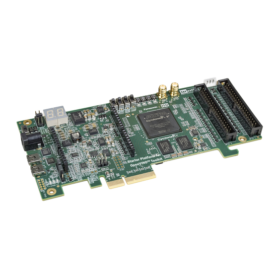
Page 7: Chapter 2 Introduction Of The C5P Board
Chapter 2 Introduction of the C5P board This chapter provides an introduction to the features and design characteristics of the C5P board. 2.1 Layout and Components Figure 2‑1 Figure 2-2 shows a photograph of the board. It depicts the layout of the board and indicates the location of the connectors and key components. -
Page 8: Block Diagram Of The C5P Board
The C5P board has many features that allow users to implement a wide range of designed circuits, from simple circuits to various multimedia projects: Intel FPGA Cyclone® V GX 5CGXFC9D6F27C7N device Serial configuration device– EPCQ256 USB-Blaster II onboard for programming; JTAG Mode ... - Page 9 Analog ADC Interface: SPI Fast through put rate:500Ksps Channel number: 8 Resolution: 12-bit Analog input range:0 ~ 4.096 V Digital IO With diode protection C5P User Manual www.terasic.com.cn April 17, 2018...
- Page 10 5 user Keys (4 general keys, 1 CPU_RESET_n) 4 user switches 4 LED Two 7-segment displays Power 12V DC Input PCIe 12V Input Cooling System 12V Fan with 5000 Rotational Speed C5P User Manual www.terasic.com.cn April 17, 2018...
-
Page 11: Chapter 3 Using The C5P Board
The information is retained within EPCQ256 even if the C5P board is turned off. When the board is powered on, the configuration data in the EPCQ256 device is automatically loaded into the Cyclone V FPGA. - Page 12 Open the Quartus II programmer under Quartus Prime Tools and click “Auto Detect”, as circled in Figure 3‑2. Figure 3‑2 Detect FPGA device in JTAG mode Figure 3‑3. Select detected device associated with the board, as circled in C5P User Manual www.terasic.com.cn April 17, 2018...
- Page 13 Right click on the FPGA device and select Change File to open the .sof file to be Figure 3‑5. programmed, as highlighted in Figure 3‑5 Open the .sof file to be programmed into the FPGA device Select the .sof file to be programmed, as shown in Figure 3‑6. C5P User Manual www.terasic.com.cn April 17, 2018...
- Page 14 Figure 3‑7 Program .sof file into the FPGA device Configure the FPGA in AS Mode The C5P board uses the EPCSQ256 device to store configuration data for the Cyclone V FPGA. This configuration data is automatically loaded from the quad...
-
Page 15: Board Status Elements
In addition to the 4 LEDs that the FPGA device can control, there are 4 indicators which Figure 3‑9, please refer the details in Table 3 can indicate the board status, as shown in ‑1. Figure 3‑9 LED Indicators on C5P C5P User Manual www.terasic.com.cn April 17, 2018... -
Page 16: Clock Circuitry
PLL circuit. Table 3‑2. The associated pin assignment for clock inputs to FPGA I/O pins is listed in Figure 3-10 Block diagram of the clock distribution on C5P Table 3‑2 Pin Assignment of Clock Inputs FPGA Pin Signal Name... -
Page 17: Peripherals Connected To The Fpga
Since the push-buttons are debounced, they can be used as reset inputs in a circuit. Figure 3-11 Connections between the push-buttons and the Cyclone V FPGA Pushbutton depressed Pushbutton released Before Debouncing Schmitt Trigger Debounced Figure 3-12 Switch debouncing C5P User Manual www.terasic.com.cn April 17, 2018... - Page 18 LED on or off, respectively. shows the connections between LEDs and Cyclone V FPGA. Table 3‑3、Table 3‑4 Table 3‑5 list the pin assignment of user push-buttons, switches, and LEDs. C5P User Manual www.terasic.com.cn April 17, 2018...
- Page 19 Generate a high logic level when 3.3-V KEY[1] PIN_K25 Input LVTTL it is not pressed. Four push- buttons (KEY0, KEY1, KEY2 and 3.3-V KEY[2] PIN_K26 Input KEY3) are debounced. LVTTL 3.3-V KEY[3] PIN_G26 Input LVTTL C5P User Manual www.terasic.com.cn April 17, 2018...
- Page 20 LVTTL 3.4.2 7-Segment Displays Figure 3-15 C5P board has two 7-segment displays. shows the connection of seven segments (common anode) to pins on Cyclone V FPGA。The segment can be turned on or off by applying a low logic level or high logic level from the FPGA, respectively. Each...
- Page 21 LVTTL 3.4.3 SDRAM Memory The C5P features 64MB of SDRAM with a single 64MB (32Mx16) SDRAM chip. The chip consists of 16-bit data line, control line, and address line connected to the FPGA. This chip uses the 3.3V LVCMOS signaling standard. Connections between the FPGA and...
- Page 22 SDRAM Bank Address[1] 3.3-V LVTTL DRAM_DQ[0] PIN_L24 Output SDRAM Data[0] 3.3-V LVTTL DRAM_DQ[1] PIN_M24 Output SDRAM Data[1] 3.3-V LVTTL DRAM_DQ[2] PIN_N23 Output SDRAM Data[2] 3.3-V LVTTL DRAM_DQ[3] PIN_K23 Output SDRAM Data[3] 3.3-V LVTTL C5P User Manual www.terasic.com.cn April 17, 2018...
- Page 23 SDRAM Row Address Strobe 3.3-V LVTTL 3.4.4 DDR3 Memory C5P supports 1GB of DDR3 SDRAM comprising of two x16 bit DDR3 devices. The signals are connected to the dedicated Hard Memory Controller for FPGA I/O banks and the target speed is 400MHz.
- Page 24 Output Differential 1.5-V DDR3_DQS_p[2] PIN_V15 DDR3 Data Strobe p[2] SSTL Class I Output Differential 1.5-V DDR3_DQS_p[3] PIN_W16 DDR3 Data Strobe p[3] SSTL Class I DDR3_DQS_n[0] PIN_W13 Output DDR3 Data Strobe n[0] Differential 1.5-V C5P User Manual www.terasic.com.cn April 17, 2018...
- Page 25 SSTL-15 Class I DDR3_DQ[26] PIN_AC20 Output DDR3 Data[26] SSTL-15 Class I DDR3_DQ[27] PIN_AD21 Output DDR3 Data[27] SSTL-15 Class I DDR3_DQ[28] PIN_AF16 Output DDR3 Data[28] SSTL-15 Class I DDR3_DQ[29] PIN_AF17 Output DDR3 Data[29] SSTL-15 Class I C5P User Manual www.terasic.com.cn April 17, 2018...
- Page 26 3.4.5 UART to USB The C5P board has one UART interface. The physical interface is implemented by UART- USB onboard bridge from a CP2102N chip to the host with a USB Mini-B connector. More information about the chip is available on the manufacturer’s website, or in the directory Figure 3‑18...
Need help?
Do you have a question about the C5P and is the answer not in the manual?
Questions and answers