Table of Contents
Advertisement
Advertisement
Table of Contents

Related Manuals for Terasic TR5


Summary of Contents for Terasic TR5
- Page 1 TR5 User Manual www.terasic.com July 27, 2017...
-
Page 2: Table Of Contents
..........................60 ONFIGURE PERATION 4.3 F ......................61 LASH ROGRAMMING WITH SERS ESIGN 4.4 R ..........................64 ESTORE ACTORY ETTINGS PROGRAMMABLE PLL CHAPTER 5 ........................65 5.1 C CDCM6208 LMK04096B RTL ....................65 ONFIGURE TR5 User Manual www.terasic.com July 27, 2017... - Page 3 8.1 F ....................... 130 UNCTION OF THE RANSCEIVER 8.2 F ....................... 130 UNCTION OF THE RANSCEIVER 8.1 T ................................132 ESTING FMC CONNECTORS PIN OUT CHAPTER 9 ....................135 ADDITIONAL INFORMATION ........................... 162 TR5 User Manual www.terasic.com July 27, 2017...
-
Page 4: Chapter 1 Overview
With an iPass PCIe gen3 connector, the TR5 is designed for the most demanding high-end applications, empowered with the Altera 28 nm Stratix V GX, delivering the best system-level integration and flexibility in the industry. - Page 5 One mini Uart to USB connector System Monitor and Control Temperature sensor Fan control Power monitor Mechanical Specification 4 FPGA Mezzanine Card (FMC) Connectors One 40-pin Expansion Header TR5 User Manual www.terasic.com July 27, 2017...
-
Page 6: Block Diagram
12V DC Input 1.3 Block Diagram Figure 1-1 shows the block diagram of the TR5 board. To provide maximum flexibility for the users, 94H94H all key components are connected with the Stratix V GX FPGA device. Thus, users can configure the FPGA to implement any system design. - Page 7 2MB ZBT SSRAM Up to 8GB DDR3 SO-DIMM SDRAM 256MB FLASH General user I/O 4 user controllable LEDs 4 user push buttons 4 user slide switches On-Board Clock TR5 User Manual www.terasic.com July 27, 2017...
- Page 8 I/O standards: 3.3V (with level shift from 2.5V to 3.3V) External PCI Express x4 iPass Connector Support for PCIe x4 Gen1/2/3 iPass connector with x4 PCI Express slot Power Source DC 12V power adapter TR5 User Manual www.terasic.com July 27, 2017...
-
Page 9: Chapter 2 Board Components
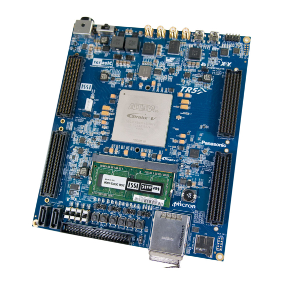
2.1 Board Overview Figure 2-1 is the top and bottom view of the TR5 development board. It depicts the layout of the 96H96H board and indicates the location of the connectors and key components. Users can refer to this figure for relative location of the connectors and key components. - Page 10 Figure 2-1 FPGA Board (Top) TR5 User Manual www.terasic.com July 27, 2017...
-
Page 11: Configuration, Status And Setup
Flash memory configuration of the FPGA using stored images from the flash memory on power- For programming by on-board USB-Blaster II, the following procedures show how to download a configuration bit stream into the Stratix V GX FPGA: TR5 User Manual www.terasic.com July 27, 2017... -
Page 12: Status Led
The Configure Mode Control DIP switch (SW5) is provided to specify the configuration mode of the FPGA. As currently only one mode is supported, please set all positions as shown in Figure 2-3. 99H99H TR5 User Manual www.terasic.com July 27, 2017... - Page 13 The Image Select DIP switch (SW4) is provided to specify the image for configuration of the FPGA. Setting SW4 to high (‘0’) specifies the default factory image to be loaded, setting SW4 to low (‘1’) specifies the TR5 to load a user-defined image, as shown in Figure 2-4.
- Page 14 2-5, make short circuit onto JP5 pin 7 and pin 8, the status of D12, D13 and D14 will be set as “ON/OFF/ON” for representing the FMCA VCCIO is 2.5V. Table 2-2, Table 2-3, Table 2-4 Table 2-5 lists the voltage settings of the FMCA~FMCD VCCIO and their corresponding LED display status. TR5 User Manual www.terasic.com July 27, 2017...
- Page 15 FMC B VCCIO Voltage Short Pin 1 & 2 1.2V Short Pin 3 & 4 1.5V Short Pin 5 & 6 1.8V Short Pin 7 & 8 2.5V(Default) Short Pin 9 & 10 3.0V TR5 User Manual www.terasic.com July 27, 2017...
- Page 16 3.0V FMC JTAG Header The TR5 supports individual JTAG interfaces on each FMC connector. This feature allows users to extend the JTAG chain to FMC daughter cards. The JTAG signals on each FMC connector can be removed or included in the active JTAG chain via 3-Pin header (See Figure 2-6).
-
Page 17: General User Input/Output
The FPGA board includes four user defined push-buttons that allow users to interact with the Stratix V GX device. Each push-button provides a high logic level or a low logic level when it is not pressed TR5 User Manual www.terasic.com... - Page 18 Stratix V GX FPGA. The LEDs are turned on or off when the associated pins are driven to a low or high logic level, respectively. A list of the pin names on the FPGA that are connected to the LEDs is given in Table 2-9. 10 5H105H TR5 User Manual www.terasic.com July 27, 2017...
- Page 19 Figure 2-7 Connection between UART-To-USB and Stratix V GX FPGA Table 2-10 UART-To-USB Pin Assignments, Schematic Signal Names, and Functions Schematic Stratix V Board Signal Description I/O Standard GX Pin Reference Name Number UART_TX UART_TX Uart TX output from FPGA 1.2/1.5/1.8/2.5/3.0- PIN_T26 TR5 User Manual www.terasic.com July 27, 2017...
- Page 20 Schematic Stratix V Signal Description I/O Standard GX Pin Name Number SD_CLK Serial Clock 1.5-V PIN_BB39 SD_CMD Command, Response 1.5-V PIN_BA36 SD_DAT0 Serial Data 0 1.5-V PIN_AV37 SD_DAT1 Serial Data 1 1.5-V PIN_AY37 TR5 User Manual www.terasic.com July 27, 2017...
-
Page 21: Temperature Sensor , Fan Control And Power Monitor
Users regulate and monitor the speed of fan depending on the measured system temperature. The TR5 has implemented a power monitor chip to monitor the board input power voltage and current. Figure 2-9 shows the connection between the power monitor chip and the Stratix V GX FPGA. The power monitor chip monitors both shunt voltage drops and board input power voltage allows user to monitor the total board power consumption. -
Page 22: Clock Circuit
2.5 Clock Circuit The development board includes one 50 MHz and two programmable clock generators. Figure 2-10 shows the default frequencies of on-board all external clocks going to the Stratix V GX FPGA. TR5 User Manual www.terasic.com July 27, 2017... - Page 23 Table 2-9 Clock Source, Signal Name, Default Frequency, Pin Assignments and Functions Stratix V Schematic Default Source I/O Standard GX Pin Application Signal Name Frequency Number CLK_50_B3B 1.5-V PIN_AW35 CLK_50_B4A 1.5-V PIN_AP10 1.2/1.5/1.8/2.5/3.0- 50.0 MHz CLK_50_B4D PIN_AY18 1.2/1.5/1.8/2.5/3.0- CLK_50_B7A PIN_M8 TR5 User Manual www.terasic.com July 27, 2017...
- Page 24 I/O standard and their 113H113H corresponding Stratix V GX device pin numbers. Table 2-10 Programmable oscillator control pin, Signal Name, I/O standard, Pin Assignments and Descriptions TR5 User Manual www.terasic.com July 27, 2017...
-
Page 25: Flash And Ssram Memory
(EPM2210) System Controller. The SSRAM also has a 16-bit data bus and share address and data bus with the flash. Figure 2-11 shows the connections between the Flash, SSRAM, MAX and Stratix V GX FPGA. TR5 User Manual www.terasic.com July 27, 2017... - Page 26 Address bus 2.5V PIN_AJ10 FSM_A10 Address bus 2.5V PIN_AF13 FSM_A11 Address bus 2.5V PIN_AE13 FSM_A12 Address bus 2.5V PIN_AJ11 FSM_A13 Address bus 2.5V PIN_BD11 FSM_A14 Address bus 2.5V PIN_AW10 FSM_A15 Address bus 2.5V PIN_AF14 TR5 User Manual www.terasic.com July 27, 2017...
- Page 27 PIN_AT12 FLASH_ADV_n Flash Address valid, active 2.5V PIN_BD26 FLASH_RDY_BSY_n Flash ready output 2.5V PIN_AU25 SSRAM_CLK SSRAM Clock 2.5V PIN_AP13 SSRAM_CKE_n SSRAM Clock enable, active 2.5V PIN_AW24 SSRAM_CE_n SSRAM Chip enable, active 2.5V PIN_AP24 TR5 User Manual www.terasic.com July 27, 2017...
-
Page 28: Ddr3 So-Dimm
DDR3 SDRAM interfaces, it is capable of running at up to 800MHz memory clock for a maximum theoretical bandwidth up to 95.4Gbps. Figure 2-12 shows the connections between the DDR3 SDRAM SO-DIMMs and Stratix V GX FPGA. TR5 User Manual www.terasic.com July 27, 2017... - Page 29 Data [6] SSTL-15 Class I PIN_AR30 DDR3_DQ7 Data [7] SSTL-15 Class I PIN_AT30 DDR3_DQ8 Data [8] SSTL-15 Class I PIN_AM29 DDR3_DQ9 Data [9] SSTL-15 Class I PIN_AN28 DDR3_DQ10 Data [10] SSTL-15 Class I PIN_AP28 TR5 User Manual www.terasic.com July 27, 2017...
- Page 30 Data [47] SSTL-15 Class I PIN_AM26 DDR3_DQ48 Data [48] SSTL-15 Class I PIN_AU28 DDR3_DQ49 Data [49] SSTL-15 Class I PIN_AU29 DDR3_DQ50 Data [50] SSTL-15 Class I PIN_AM28 DDR3_DQ51 Data [51] SSTL-15 Class I PIN_AL27 TR5 User Manual www.terasic.com July 27, 2017...
- Page 31 Address [0] SSTL-15 Class I PIN_AM32 DDR3_A1 Address [1] SSTL-15 Class I PIN_AF31 DDR3_A2 Address [2] SSTL-15 Class I PIN_AJ33 DDR3_A3 Address [3] SSTL-15 Class I PIN_AE31 DDR3_A4 Address [4] SSTL-15 Class I PIN_AP33 TR5 User Manual www.terasic.com July 27, 2017...
-
Page 32: Fmc Connectors
The FPGA Mezzanine Card (FMC) interface provides a mechanism to extend the peripheral-set of an FPGA host board by means of add-on daughter cards, which can address today’s high speed signaling requirements as well as low-speed device interface support. The FMC interfaces support JTAG, clock TR5 User Manual www.terasic.com July 27, 2017... -
Page 33: Fmc Connector
The detailed specifications of the FMC connectors are described below: 4 FMC Connector There are four FMC connectors on the TR5 board are: FMCA, FMCB, FMCC, FMCD. Both FMCA and FMCD are High Pin Count (HPC) size of connectors and FMCB and FMCC are Low Pin Count... - Page 34 Figure 2-13 FMC connectors on TR5 board Figure 2-14 Pin-Out of the high pin count FMC connector TR5 User Manual www.terasic.com July 27, 2017...
- Page 35 Figure 2-15 Pin-Out of the low pin count FMC connector Clock Interface Due to the limitation of the FPGA clock input pin numbers, not all the FMC ports have same clock interface. TR5 User Manual www.terasic.com July 27, 2017...
- Page 36 Table 2-15 shows the FPGA dedicated clock input pin placement on each FMC port. TR5 User Manual www.terasic.com July 27, 2017...
- Page 37 Please note that, all the dedicated clock pin of the FPGA are connected to external termination resistors (See Figure 2-16 ). IF users want to us these I/O as single-end standard, pleaser remove these resistors. Figure 2-16 Termination resistors on FMC clock I/Os TR5 User Manual www.terasic.com July 27, 2017...
-
Page 38: Power Supply
FMC can remove these fuses to cut the power on connector. CAUTION. Before powering on the TR5 board with a daughter card, please check to see if there is a short circuit between the power pins and FPGA I/O. - Page 39 Figure 2-17 JTAG Chain for a Standalone TR5 Component Information of the FMC Connector Table 2-17 shows the manufacture and part numbers of the FMC connector. Table 2-17 Component information of the FMC connector Connector Type Manufacturer Part Number...
-
Page 40: Sata
SATA and Stratix V GX FPGA. 124H124H Figure 2-18 Connection between the SATA and Stratix V GX FPGA Table 2-18, list the SATA pin assignments and signal names relative to the Stratix V GX device. 125H125H TR5 User Manual www.terasic.com July 27, 2017... -
Page 41: Gpio
1.4-V PCML PIN_BB2 2.10 GPIO The TR5 Board provides a 40-pin expansion header. The header connects directly to 36 pins of the Stratix V GX FPGA, and also provides DC +5V (VCC5), DC +3.3V (VCC3P3), and two GND pins. Figure 2-19 shows the I/O distribution of the GPIO connector. - Page 42 2.5V PIN_AU36 DATA[0] GPIO[1] GPIO Connection 2.5V PIN_AE36 DATA[1] GPIO[2] GPIO Connection 2.5V PIN_AF35 DATA[2] GPIO[3] GPIO Connection 2.5V PIN_AE35 DATA[3] GPIO[4] GPIO Connection 2.5V PIN_AN36 DATA[4] GPIO[5] GPIO Connection 2.5V PIN_AP36 DATA[5] TR5 User Manual www.terasic.com July 27, 2017...
- Page 43 2.5V PIN_AL21 DATA[21] GPIO[22] GPIO Connection 2.5V PIN_AN23 DATA[22] GPIO[23] GPIO Connection 2.5V PIN_AU23 DATA[23] GPIO[24] GPIO Connection 2.5V PIN_AR24 DATA[24] GPIO[25] GPIO Connection 2.5V PIN_BA25 DATA[25] GPIO[26] GPIO Connection 2.5V PIN_AR23 DATA[26] TR5 User Manual www.terasic.com July 27, 2017...
-
Page 44: Pci Express
DATA[35] 2.11 PCI Express The TR5 development board features one PCIe Express downstream interfaces (x4 lane) which are designed to interface with a PC motherboard x4 slot via PCIe cable and PCIe adapter card. Utilizing built-in transceivers on a Stratix V GX device, it is able to provide a fully integrated PCI Express- compliant solution for multi-lane (x4) applications. - Page 45 2-22) will be used to connect TR5 board and PCIe add-in card as shown Figure 2-23, the longest length is up to 3 meters. These two associated devices are not included in TR5 kit. To purchase the PCA card as well as the external cable, please refer to Terasic website pca.terasic.com and PCIe_Cable.terasic.com.
- Page 46 Figure 2-22 PCIe External Cable Figure 2-23 PCIe Link Setup between TR5 and PC Figure 2-24 PCI Express Pin Connection Table 2-22 summarizes the PCI Express pin assignments of the signal names relative to the Stratix 128H128H TR5 User Manual www.terasic.com...
- Page 47 PIN_BA41 PCIE_TX_p[2] PCIe Transmitter data p2 1.4-V PCML PIN_AT39 PCIE_RX_p[2] PCIe Receiver data p2 1.4-V PCML PIN_AW41 PCIE_TX_p[3] PCIe Transmitter data p3 1.4-V PCML PIN_AU41 PCIE_RX_p[3] PCIe Receiver data p3 1.4-V PCML PIN_AY43 TR5 User Manual www.terasic.com July 27, 2017...
-
Page 48: Chapter 3 System Builder
Board damaged for wrong pin/bank voltage assignment. Board malfunction caused by wrong device connections or missing pin counts for connected ends. Performance that has dropped because of improper pin assignments. TR5 User Manual www.terasic.com July 27, 2017... -
Page 49: General Design Flow
The Quartus II setting file contains information such as FPGA device type, top-level pin assignment, and I/O standard for each user-defined I/O pin. Finally, the Quartus II programmer must be used to download SOF file to the FPGA board using JTAG interface. TR5 User Manual www.terasic.com July 27, 2017... -
Page 50: Using System Builder
The System Builder is located in the directory: "Tools\SystemBuilder" in the System CD. Users can copy the whole folder to a host computer without installing the utility. Before using the System Builder, execute the SystemBuilder.exe on the host computer as appears in Figure 3-2. TR5 User Manual www.terasic.com July 27, 2017... - Page 51 Select the target board type (TR5_A7 or TR5_AB ) and input project name as show in Figure 3-3. Project Name: Specify the project name as it is automatically assigned to the name of the top-level design entity. TR5 User Manual www.terasic.com July 27, 2017...
-
Page 52: System Configuration
If the component is enabled, the System Builder will automatically generate the associated pin assignments including the pin name, pin location, pin direction, and I/O standards. TR5 User Manual www.terasic.com July 27, 2017... - Page 53 DDR3 SDRAM demonstration in Chapter 6. Figure 3-4 System Configuration Group Programmable PLL There are two external plls on-board that provide reference clocks for the following signals: FMCA_ONBOARD_REFCLK FMCD_ONBOARD_REFCLK PCIE_ONBOARD_REFCLK TR5 User Manual www.terasic.com July 27, 2017...
- Page 54 Verilog which facilitates users’ implementation as no additional control code is required to configure the programmable oscillator. Note: If users need to dynamically change the frequency, they would need to modify the generated control code themselves. TR5 User Manual www.terasic.com July 27, 2017...
- Page 55 The System Builder also provides functions to restore default setting, loading a setting, and saving users’ board configuration(s) file, as shown in Figure 3-6. Users can save the current board configuration information into a .cfg file and load it to the System Builder. TR5 User Manual www.terasic.com July 27, 2017...
- Page 56 Table 3-1 The files generated by System Builder No. Filename Description <Project name>.v Top level Verilog file for Quartus II CDCM6208_controller (*) CDCM6208 External PLL controller IP TR5 User Manual www.terasic.com July 27, 2017...
- Page 57 Users can use Quartus II software to add custom logic into the project and compile the project to generate the SRAM Object File (.sof). For CDCM6208, the Controller will be instantiated in the Quartus II top-level file as listed below: TR5 User Manual www.terasic.com July 27, 2017...
- Page 58 For LMK04096B, the Controller will be instantiated in the Quartus II top-level file as listed below: TR5 User Manual www.terasic.com July 27, 2017...
- Page 59 If dynamic configuration for the oscillator is required, users need to modify the code according to users’ desired behavior. TR5 User Manual www.terasic.com July 27, 2017...
-
Page 60: Chapter 4 Flash Programming
Before programming, users need to bundle their .sof files and NIOS II .elf files together and then convert them into the .pof file which is used by the Convert TR5 User Manual www.terasic.com July 27, 2017... -
Page 61: Fpga Configure Operation
4. Power on the FPGA board or press MAX_RST button if board is already powered on 5. When configuration is completed, the green Configure Done LED D21 will light. If there is error, the red Configure Error LED D23 will light. Figure 4-1 MSEL[0:4] set to “00000” TR5 User Manual www.terasic.com July 27, 2017... -
Page 62: Flash Programming With Users Design
Translate .elf into .hex file output_file.cof input file for convert program_flash.cdf Input file for download factory.sof Factory Hardware design file for Hello Demo factory.elf Factory Software design file for Hello Demo user.sof User Hardware design file TR5 User Manual www.terasic.com July 27, 2017... - Page 63 NIOS II program can be boot from flash successfully: 1. QSYS should include a Flash controller for the CFI Flash on the development board. Please ensure that the base address of the controller is 0x00, as shown in Figure 4-5. TR5 User Manual www.terasic.com July 27, 2017...
- Page 64 4-6. Figure 4-5 Flash Controller Settings in QSYS Figure 4-6 Reset Vector Settings for NIOS II Processor For implementation detail, users can refer the Hello example located in the CD folder: Demonstrations/ Hello TR5 User Manual www.terasic.com July 27, 2017...
-
Page 65: Restore Factory Settings
Flash Loader) Option Bits data into the address 0x30000. The option bits data specifies 0x2940000 as start address of your hardware design. The Quartus II program tool quartus_pgm programs the Flash based on the Parallel FlashLoader design in the FPGA. TR5 User Manual www.terasic.com July 27, 2017... -
Page 66: Chapter 5 Programmable Pll
The source codes and tool of these examples are all available on the System CD. 5.1 Configure CDCM6208 and LMK04096B in RTL There are two clock generators: CDCM6208 and LMK04096B on TR5 FPGA board can provide adjustable frequency reference clock (See Figure 5-1) for FMC, SATA , DDR3 and PCIE interfaces, etc. - Page 67 Figure 5-2), all the clock channels controlled by 150H15 0H the CDCM6208 and LMK0496B will be active and numbers of the frequencies can be chosen. Figure 5-2 Enable CDCM6208 clock on System Builder TR5 User Manual www.terasic.com July 27, 2017...
- Page 68 = `CDCM6208_MODE_0; .rst_n(lmk04906_reset_n), assign cdcm6208_freq_disable .iFREQ_SELECT(lmk04906_freq_select), `CDCM6208_FMCA_DISABLE_BIT // spi `CDCM6208_FMCD_DISABLE_BIT .LMK04906_CLK(LMK04906_CLK), `CDCM6208_SATA_HOST_DISABLE_BIT .LMK04906_DATAIN(LMK04906_DATAIN), `CDCM6208_SATA_DEVICE_DISABLE_BIT .LMK04906_LE(LMK04906_LE), `CDCM6208_PCIE_DISABLE_BIT .SPI_DONE(lmk04906_spi_done) `CDCM6208_DDR3_DISABLE_BIT; I2C_CDCM6208_Config I2C_CDCM6208_Config_inst( .iCLK(OSC_50_B3B), //50MHZ .iRST_N(cdcm6208_reset_n), .iFREQ_SELECT(cdcm6208_freq_select), .iFREQ_DISABLE(cdcm6208_freq_disable), // i2c .I2C_SCLK(CLOCK_SCL), .I2C_SDAT(CLOCK_SDA), .I2C_DONE(cdcm6208_i2c_done) ); TR5 User Manual www.terasic.com July 27, 2017...
- Page 69 Port Direction Description iCLK input System Clock (50Mhz) Synchronous Reset (0: Module Reset, 1: iRST_n input Normal) iFREQ_DISABLE input Disable the CDCM6208 output frequency Setting CDCM6208 Output Channel Frequency iFREQ_SELECT input combination mode TR5 User Manual www.terasic.com July 27, 2017...
- Page 70 1. Firstly, download ClockBuider Pro Software(See Figure 5-4), which is provided by TI. This tool can help users to set the CDCM6208’s output frequency of each channel through the GUI TR5 User Manual www.terasic.com July 27, 2017...
- Page 71 Register parameters required for each frequency. The tool download link: http://www.ti.com/lit/sw/scac134d/scac134d.zip Figure 5-4 ClockBuilder Pro Wizard 2. After the installation, select CDCM6208, and configure the input frequency and output frequency as shown in Figure 5-5. TR5 User Manual www.terasic.com July 27, 2017...
- Page 72 Figure 5-5 Define Output Clock Frequencies on CDCM6208 EVM Software 3. After the setting is completed, CDCM6208 EVM Software generates a register table, which contains users setting frequency corresponding register value (See Figure 5-6). TR5 User Manual www.terasic.com July 27, 2017...
- Page 73 Figure 5-6 Open Register Table on CDCM6208 EVM Software 4. Open CDCM6208 control IP sub-module “I2C_CDCM6208_Config.v “as shown in Figure 5-7, refer to Register Table to modify all the sub-module corresponding register values (See Figure 5-8). Figure 5-7 Sub-Module file "I2C_CDCM6208_Config.v" TR5 User Manual www.terasic.com July 27, 2017...
- Page 74 (2) After manually modifying, please remember to modify the clock constrain setting in .SDC file. Using LMK04096B control IP Table 5-3 lists the instruction ports of LMK04096B Controller IP. Table 5-3 LMK04096B Controller Instruction Ports TR5 User Manual www.terasic.com July 27, 2017...
- Page 75 322.265625 644.53125 322.265625 322.265625 4'd5 322.265625 644.53125 322.265625 644.53125 4'd6 322.265625 644.53125 644.53125 322.265625 4'd7 322.265625 644.53125 644.53125 644.53125 4'd8 644.53125 322.265625 322.265625 322.265625 4'd9 644.53125 322.265625 322.265625 644.53125 4'd10 644.53125 322.265625 644.53125 322.265625 TR5 User Manual www.terasic.com July 27, 2017...
- Page 76 LMK04096B’s output frequency of each channel through the GUI interface, and it will automatically calculate the Register parameters required for each frequency. The tool download link: http://www.ti.com/tool/codeloader?keyMatch=CodeLoader&tisearch=Search-EN- Everything TR5 User Manual www.terasic.com July 27, 2017...
- Page 77 Figure 5-9 Codeloader 6. After the installation, select LMK04096B, and configure the input frequency and the output frequency as shown in Figure 5-10. TR5 User Manual www.terasic.com July 27, 2017...
- Page 78 Figure 5-10 Define Output Clock Frequencies on Codeloader 7. After the setting is completed, CodeLoader generates a Register Table, which contains users setting frequency corresponding register values (See Figure 5-11). TR5 User Manual www.terasic.com July 27, 2017...
- Page 79 Figure 5-11 Open Register Table on Codeloder 8. Open LMK04096B control IP sub-module “SPI_LMK04906_Config.v “as shown in Figure 5-12, refer Design Report parameter to modify all the sub-module corresponding register values (See Figure 5-13). TR5 User Manual www.terasic.com July 27, 2017...
- Page 80 Figure 5-12 Sub-Module file " SPI_LMK04906_Config.v" Figure 5-13 Modify LMK04096B Control IP Based on the Design Report TR5 User Manual www.terasic.com July 27, 2017...
-
Page 81: Nios Ii Control For Pll/Temperature/Power
I2C protocol which is implemented in the C code. The LMK04096B is controlled by the Nios II through the SPI controller. The Nios II program is running in the on-chip memory. TR5 User Manual www.terasic.com July 27, 2017... - Page 82 FPGA temperature, and the local temperature is the board temperature where the temperature sensor located (or at the temperature sensors location). A power monitor IC (INA230AIRGTT) embedded on the board can monitor TR5 real-time current TR5 User Manual www.terasic.com...
- Page 83 This IC can work out current/power value as multiplier and divider are embedded in it. There is a shunt resistor R35 (RSHUNT =0.003 Ω) for INA230AIRGTT in the circuit, when the TR5 board is powered on, there will be a voltage drop (named Shut Voltage) on R35. Based on sense resistors, the program of the power monitor can calculate the associated voltage, current and power consumption from the IN230 through the I2C interface.
- Page 84 FMCA/FMCD/DDR3/PCIE/SATA, as shown in Figure 5-18. For programmable PLL LMK04906 test, please input key ‘3’ and press ‘Enter’ in the nios- terminal, as shown in Figure 5-19. Figure 5-16 Temperature Demo TR5 User Manual www.terasic.com July 27, 2017...
- Page 85 Figure 5-17 power monitor Demo Figure 5-18 CDCM6208 Demo TR5 User Manual www.terasic.com July 27, 2017...
- Page 86 Figure 5-19 LMK04906 Demo TR5 User Manual www.terasic.com July 27, 2017...
-
Page 87: Examples Of Advanced Demonstration
This chapter introduces several advanced designs that demonstrate Stratix V GX features using the TR5 board. The provided designs include the major features on the board; such as the DDR3, fan control and USB to Uart interface. For each demonstration the Stratix V GX FPGA configuration file is provided, as well as full source code in Verilog HDL. - Page 88 Demonstration Source Code Quartus II project directory: TR5_Flash_SSRAM Nios II Eclipse: TR5_Flash_SSRAM\software Nios Project Compilation Before you attempt to compile the reference design under Nios II Eclipse, make sure the project is TR5 User Manual www.terasic.com July 27, 2017...
- Page 89 After the Nios II program is downloaded and executed successfully, a prompt message will be displayed in the nios2-terminal. The program will display progressing and resulting information, as shown in Figure 6-2. TR5 User Manual www.terasic.com July 27, 2017...
-
Page 90: Ddr3 Sdram Test
6.2 DDR3 SDRAM Test This demonstration performs a memory test function for two DDR3-SDRAM SO-DIMMs by RTL code on the TR5. The memory size of each DDR3 SDRAM SO-DIMM used in this test is 2 GB. Function Block Diagram Figure 6-3 shows the function block diagram of this demonstration. - Page 91 4. Go to the Quartus II menu and select Tools -> TCL Scripts … to run the TCL files generated by the DDR3 IP. Design Tools 64-bit Quartus II v16.0 Demonstration Source Code Project Directory: Demonstration\DDR3_Test Bit Stream: DDR3_Test.sof TR5 User Manual www.terasic.com July 27, 2017...
- Page 92 Make sure Quartus II is installed on the host PC. Connect the TR5 board to the host PC via the USB cable. Install the USB-Blaster II driver if necessary. Install the DDR3 SODDIM and Power on the TR5 board.
-
Page 93: Ddr3 Sdram Test By Nios Ii
SDRAM. In the QSYS, Nios II and the On-Chip memory are designed running with the 200 MHz clock, and the Nios II program is running in the on-chip memory. A PIO Controller is used to monitor buttons status which is used to trigger starting memory testing. TR5 User Manual www.terasic.com July 27, 2017... - Page 94 3. Perform “Analysis and Synthesis” by selecting from the Quartus II menu: ProcessStartStart Analysis & Synthesis. 4. Run the TCL files generated by DDR3 IP by selecting from the Quartus II menu: ToolsTCL Scripts… Design Tools TR5 User Manual www.terasic.com July 27, 2017...
- Page 95 Make sure the DDR3 SODIMMs are installed on the FPGA board. Power on the FPGA board. Use the USB Cable to connect PC and the FPGA board and install USB Blaster II driver if necessary. TR5 User Manual www.terasic.com July 27, 2017...
-
Page 96: Fan Speed Control
The following section will save lots of time for the development of user application. System Block Diagram Figure 6-6 shows the system block diagram of this demo. It is necessary to configure the MAX6650 TR5 User Manual www.terasic.com July 27, 2017... - Page 97 The status of BIT 4 ~ 7 can be ignored because BIT 4 is for MAX6651 only and BIT 5 ~ 7 are always low. TR5 User Manual www.terasic.com July 27, 2017...
- Page 98 Demonstration Setup Make sure Quartus II is installed on the host PC. Connect the TR5 and the host PC via the USB cable. Install the USB-Blaster II driver if necessary. TR5 User Manual www.terasic.com July 27, 2017...
-
Page 99: Uart To Usb Control
RS232 which needs to connect to a RS232 cable. But today many personal computers don't have the RS232 connector which makes it very inconvenient to develop projects. The TR5 board is designed to support UART communication through a USB cable. The UART to USB circuit is responsible for converting the data format. - Page 100 Before you attempt to compile the reference design under Nios II Eclipse, make sure the project is cleaned first by clicking ‘Clean’ from the ‘Project’ menu of Nios II Eclipse. Demonstration Batch File Demo Batch File Folder: uart_control\demo_batch TR5 User Manual www.terasic.com July 27, 2017...
- Page 101 Connect a USB cable between your computer and the USB connector (J5) on the TR5 board. Power on your TR5 board, if you find an unrecognized USB Serial Port in Device Manager as shown in Figure 6-8 .you should install the UART to the USB driver before you run the demonstration.
- Page 102 Open the putty software, type in the parameter as shown in Figure 6-10 and click open button to open the terminal.(Here is a link for you to download the putty terminal: Download Putty Figure 6-10 putty terminal setup TR5 User Manual www.terasic.com July 27, 2017...
- Page 103 Make sure Quartus II and Nios II are installed on your PC. Connect USB Blaster to the TR5 board (J6) and install USB Blaster driver if necessary. Execute the demo batch file “ test.bat” under the batch file folder uart_control\demo_batch.
-
Page 104: Pci Express Reference Design
FPGA System and PC System. The FPGA System is developed based on V-Series Avalon-MM DMA for PCI Express. The application software on the PC side is developed by Terasic based on Altera’s PCIe kernel mode driver. TR5 User Manual www.terasic.com... -
Page 105: Pc Pci Express Software Sdk
The kernel mode driver assumes the PCIe vender ID (VID) is 0x1172 and the device ID (DID) is 0xE003. If different VID and DID are used in the design, users need to modify the PCIe vender ID (VID) and device ID (DID) in the driver INF file accordingly. TR5 User Manual www.terasic.com July 27, 2017... - Page 106 The PCI Express driver incorporated in the DLL library is called TERASIC_PCIE_AVMM.dll. Users can develop their applications based on this DLL. The altera_pcie_win_driver.sys kernel driver is provided by Altera. Figure 7-2 PCI Express Software Stack TR5 User Manual www.terasic.com July 27, 2017...
- Page 107 To install the PCI Express driver, execute the steps below: 1. Make sure the TR5 and the PC are both powered off. 2. Plug the PCIe adapter card into the PCIe slot on the PC motherboard. Use the PCIe cable to...
- Page 108 3. Power on your TR5 board and the host PC 4. Make sure Altera Programmer and USB-Blaster II driver are installed 5. Execute test.bat in “CDROM\Demonstrations\PCIe_Fundamental\demo_batch” to configure the FPGA 6. Restart windows operation system 7. Click the Control Panel menu from the Windows Start menu. Click the Hardware and the Sound item before clicking the Device Manager to launch the Device Manager dialog.
- Page 109 Figure 7-5 Dialog of Browse my computer for driver software 9. In the Browse for driver software on your computer dialog, click the Browse button to specify the folder where altera_pcie_din_driver.inf is located, as shown in Figure 7-6 Click the Next button. TR5 User Manual www.terasic.com July 27, 2017...
- Page 110 10. When the Windows Security dialog appears, as shown Figure 7-7 , click the Install button. Figure 7-7 Click Install in the dialog of Windows Security 11. When the driver is installed successfully, the successfully dialog will appears, as shown in TR5 User Manual www.terasic.com July 27, 2017...
- Page 111 Figure 7-8 Click Close when the installation of Altera PCI API Driver is complete 12. Once the driver is successfully installed, users can see the Altera PCI API Driver under the device manager window, as shown in Figure 7-9. TR5 User Manual www.terasic.com July 27, 2017...
- Page 112 Copy TERASIC_PCIE_AVMM.DLL to the folder where the project.exe is located. Dynamically load TERASIC_PCIE_AVMM.DLL in C/C++ program. To load the DLL, please refer to the PCIe fundamental example below. Call the SDK API to implement the desired application. TR5 User Manual www.terasic.com July 27, 2017...
- Page 113 Users need to call PCIE_Close to release handle once the handle is no more used. PCIE_Close Function: Close a handle associated to the PCIe card. Prototype: void PCIE_Close( PCIE_HANDLE hPCIE); Parameters: hPCIE: TR5 User Manual www.terasic.com July 27, 2017...
- Page 114 Return TRUE if read data is successful; otherwise FALSE is returned. PCIE_Write32 Function: Write a 32-bit data to the FPGA Board. Prototype: bool PCIE_Write32( PCIE_HANDLE hPCIE, PCIE_BAR PcieBar, PCIE_ADDRESS PcieAddress, DWORD dwData); TR5 User Manual www.terasic.com July 27, 2017...
- Page 115 A pointer to a memory buffer to retrieved the data from FPGA. The size of buffer should be equal or larger the dwBufSize. dwBufSize: Specify the byte number of data retrieved from FPGA. Return Value: Return TRUE if read data is successful; otherwise FALSE is returned. TR5 User Manual www.terasic.com July 27, 2017...
- Page 116 Return TRUE if write data is successful; otherwise FALSE is returned. PCIE_ConfigRead32 Function: Read PCIe Configuration Table. Read a 32-bit data by given a byte offset. Prototype: bool PCIE_ConfigRead32 ( PCIE_HANDLE hPCIE, DWORD Offset, DWORD *pdwData Parameters: TR5 User Manual www.terasic.com July 27, 2017...
-
Page 117: Reference Design - Fundamental
Windows Application Software folder : windows_app, includes PCIE_FUNDAMENTAL.exe TERASIC_PCIE_AVMM.dll Demonstration Setup 1. Use the PCIe cable to connect to the TR5 PCIE connector and PCIe adapter card as shown in TR5 User Manual www.terasic.com July 27, 2017... - Page 118 3. Install PCIe driver if necessary. The driver is located in the folder: CDROM\Demonstration \PCIe_SW_KIT\PCIe_Driver. 4. Restart Windows 5. Make sure the Windows has detected the FPGA Board by checking the Windows Control panel as shown in Figure 7-11. TR5 User Manual www.terasic.com July 27, 2017...
- Page 119 7. Type 0 followed by a ENTER key to select Led Control item, then input 15 (hex 0x0f) will make all led on as shown in Figure 7-13. If input 0(hex 0x00), all led will be turned off. TR5 User Manual www.terasic.com July 27, 2017...
- Page 120 Figure 7-14. Figure 7-14 Screenshot of Button Status Report 9. Type-2 followed by an ENTER key to select DMA Testing item. The DMA test result will be report as shown in Figure 7-15. TR5 User Manual www.terasic.com July 27, 2017...
- Page 121 10. Type 99 followed by an ENTER key to exit this test program Development Tools Quartus II 16.0 Visual C++ 2012 Demonstration Source Code Location Quartus Project: Demonstrations\PCIE_Fundamental Visual C++ Project: Demonstrations\PCIe_SW_KIT\PCIE_FUNDAMENTAL TR5 User Manual www.terasic.com July 27, 2017...
- Page 122 Figure 7-16 Hardware block diagram of the PCIe reference design Windows Based Application Software Design The application software project is built by Visual C++ 2012. The project includes the following major files: Name Description TR5 User Manual www.terasic.com July 27, 2017...
- Page 123 The PCI express driver is loaded successfully. The LED control is implemented by calling PCIE_Write32 API, as shown below: The button status query is implemented by calling the PCIE_Read32 API, as shown below: TR5 User Manual www.terasic.com July 27, 2017...
-
Page 124: Pcie Reference Design - Ddr3
Windows Application Software folder : windows_app, includes PCIE_DDR3.exe TERASIC_PCIE_AVMM.dll Demonstration Setup 1. Install both DDR3 1600 2GB SODIMM on the FPGA board. 2. Install the FPGA board on your PC. TR5 User Manual www.terasic.com July 27, 2017... - Page 125 8. Type 2 followed by the ENTER key to select Link Info item. The PICe link information will be shown as in Figure 7-18. Gen2 link speed and x4 link width are expected. Figure 7-18 Screenshot of Link Info TR5 User Manual www.terasic.com July 27, 2017...
- Page 126 Figure 7-19 Screenshot of On-Chip Memory DMA Test Result 10. Type-4 followed by the ENTER key to select DMA DDR3 SODIMM Memory Test item. The DMA write and read test result will be report as shown in Figure 7-20. TR5 User Manual www.terasic.com July 27, 2017...
- Page 127 LED and monitor the Button Status, and the On-Chip memory and DDR3 SOSIMM Memory are used for performing DMA testing. The PIO controllers、the On-Chip memory and DDR3 SOSIMM Memory are connected to the PCI Express Hard IP controller through the Memory-Mapped Interface. TR5 User Manual www.terasic.com July 27, 2017...
- Page 128 Implement dynamically load for TERAISC_PCIE_AVMM.DLL PCIE.h TERASIC_PCIE_AVMM.h SDK library file, defines constant and data structure The main program PCIE_DDR3.cpp includes the header file "PCIE.h" and defines the controller address according to the FPGA design. TR5 User Manual www.terasic.com July 27, 2017...
- Page 129 The LED control is implemented by calling PCIE_Write32 API, as shown below: The button status query is implemented by calling the PCIE_Read32 API, as shown below: The memory-mapped memory read and write test is implemented by PCIE_DmaWrite and PCIE_DmaRead API, as shown below: TR5 User Manual www.terasic.com July 27, 2017...
- Page 130 The pcie link information is implemented by PCIE_ConfigRead32 API, as shown below: TR5 User Manual www.terasic.com July 27, 2017...
-
Page 131: Chapter 8 Transceiver Verification
Transceiver Verification This chapter describes how to verify the FPGA transceivers for the SATA and FMC XCVRs by using the test code provided in the TR5 system CD. 8.1 Function of the Transceiver Test Code The transceiver test code is used to verify the transceiver channels for the SATA and FMC XCVR ports through an external loopback method. - Page 132 Figure 8-1 SATA Cable Figure 8-2 SATA Cable Figure 8-3 shows the FPGA board with SATA Cable four FMC Loopback Cards installed. TR5 User Manual www.terasic.com July 27, 2017...
-
Page 133: Testing
Nios-Terminal, as shown in Figure 8-4. To terminate the test, press one of the BUTTON0~3 buttons on the FPGA board. The loopback test will terminate and show the summary test results as shown in Figure 8-5. TR5 User Manual www.terasic.com July 27, 2017... - Page 134 Figure 8-4 Transceiver Loopback Test in Progress TR5 User Manual www.terasic.com July 27, 2017...
- Page 135 Figure 8-5 Transceiver Loopback Done TR5 User Manual www.terasic.com July 27, 2017...
-
Page 136: Fmc Connectors Pin Out
Chapter 9 FMC Connectors Pin Out This chapter gives all the pin assignments of the FMC connectors on the TR5. Table 9-1 FMCA (HPC) Pin Assignments, Schematic Signal Names, and Functions Schematic Stratix V GX Pin Description I/O Standard Signal Name... - Page 137 FMCA LA bank tx 1.2/1.5/1.8/2.5/3.0V/LVDS FMCA_LA_TX_n14 data n14 PIN_D24 FMCA LA bank tx 1.2/1.5/1.8/2.5/3.0V/LVDS FMCA_LA_TX_p15 data p15 PIN_E23 FMCA LA bank tx 1.2/1.5/1.8/2.5/3.0V/LVDS FMCA_LA_TX_n15 data n15 PIN_D23 FMCA_LA_TX_p16 FMCA LA bank tx 1.2/1.5/1.8/2.5/3.0V/LVDS PIN_B19 TR5 User Manual www.terasic.com July 27, 2017...
- Page 138 FMCA LA bank rx 1.2/1.5/1.8/2.5/3.0V/LVDS FMCA_LA_RX_p7 data p7 PIN_T20 FMCA LA bank rx 1.2/1.5/1.8/2.5/3.0V/LVDS FMCA_LA_RX_n7 data n7 PIN_T19 FMCA LA bank rx 1.2/1.5/1.8/2.5/3.0V/LVDS FMCA_LA_RX_p8 data p8 PIN_C31 FMCA_LA_RX_n8 FMCA LA bank rx 1.2/1.5/1.8/2.5/3.0V/LVDS PIN_B31 TR5 User Manual www.terasic.com July 27, 2017...
- Page 139 FMCA HA bank 1.2/1.5/1.8/2.5/3.0V/LVDS FMCA_HA_TX_n1 tx data n1 PIN_W31 FMCA HA bank 1.2/1.5/1.8/2.5/3.0V/LVDS FMCA_HA_TX_p2 tx data p2 PIN_W28 FMCA HA bank 1.2/1.5/1.8/2.5/3.0V/LVDS FMCA_HA_TX_n2 tx data n2 PIN_V28 FMCA_HA_TX_p3 FMCA HA bank 1.2/1.5/1.8/2.5/3.0V/LVDS PIN_R27 TR5 User Manual www.terasic.com July 27, 2017...
- Page 140 FMCA HA bank 1.2/1.5/1.8/2.5/3.0V/LVDS FMCA_HA_RX_p0 rx data p0 PIN_Y30 FMCA HA bank 1.2/1.5/1.8/2.5/3.0V/LVDS FMCA_HA_RX_n0 rx data n0 PIN_Y29 FMCA HA bank 1.2/1.5/1.8/2.5/3.0V/LVDS FMCA_HA_RX_p1 rx data p1 PIN_W32 FMCA_HA_RX_n1 FMCA HA bank 1.2/1.5/1.8/2.5/3.0V/LVDS PIN_V31 TR5 User Manual www.terasic.com July 27, 2017...
- Page 141 FMCA HA bank 1.2/1.5/1.8/2.5/3.0V/LVDS FMCA_HA_RX_n10 rx data n10 PIN_D29 FMCA HB bank 1.2/1.5/1.8/2.5/3.0V/LVDS FMCA_HB_TX_CLK_p tx clock positive PIN_B23 FMCA HB bank 1.2/1.5/1.8/2.5/3.0V/LVDS FMCA_HB_TX_CLK_n tx clock negative PIN_A23 FMCA_HB_TX_p0 FMCA HB bank 1.2/1.5/1.8/2.5/3.0V/LVDS PIN_N28 TR5 User Manual www.terasic.com July 27, 2017...
- Page 142 FMCA HB bank 1.2/1.5/1.8/2.5/3.0V/LVDS FMCA_HB_TX_p9 tx data p9 PIN_A29 FMCA HB bank 1.2/1.5/1.8/2.5/3.0V/LVDS FMCA_HB_TX_n9 tx data n9 PIN_A28 FMCA HB bank 1.2/1.5/1.8/2.5/3.0V/LVDS FMCA_HB_TX_p10 tx data p10 PIN_B17 FMCA_HB_TX_n10 FMCA HB bank 1.2/1.5/1.8/2.5/3.0V/LVDS PIN_A17 TR5 User Manual www.terasic.com July 27, 2017...
- Page 143 FMCA HB bank 1.2/1.5/1.8/2.5/3.0V/LVDS FMCA_HB_RX_n7 rx data n7 PIN_K25 FMCA HB bank 1.2/1.5/1.8/2.5/3.0V/LVDS FMCA_HB_RX_p8 rx data p8 PIN_F26 FMCA HB bank 1.2/1.5/1.8/2.5/3.0V/LVDS FMCA_HB_RX_n8 rx data n8 PIN_E27 FMCA_HB_RX_p9 FMCA HB bank 1.2/1.5/1.8/2.5/3.0V/LVDS PIN_C25 TR5 User Manual www.terasic.com July 27, 2017...
- Page 144 PIN_R41 FMCA Receiver 1.4-V PCML FMCA_DP_M2C_p2 DP 2 PIN_V43 FMCA 1.4-V PCML FMCA_DP_C2M_p3 Transmitter DP 3 PIN_N41 FMCA Receiver 1.4-V PCML FMCA_DP_M2C_p3 DP 3 PIN_T43 FMCA 1.4-V PCML FMCA_DP_C2M_p4 Transmitter DP 4 PIN_J41 TR5 User Manual www.terasic.com July 27, 2017...
- Page 145 FMCB LA bank tx FMCB_LA_TX_n0 1.2/1.5/1.8/2.5/3.0V/LVDS data n0 PIN_P32 FMCB LA bank tx 1.2/1.5/1.8/2.5/3.0V/LVDS FMCB_LA_TX_p1 data p1 PIN_V34 FMCB LA bank tx 1.2/1.5/1.8/2.5/3.0V/LVDS FMCB_LA_TX_n1 data n1 PIN_V33 FMCB LA bank tx 1.2/1.5/1.8/2.5/3.0V/LVDS FMCB_LA_TX_p2 data p2 PIN_W35 TR5 User Manual www.terasic.com July 27, 2017...
- Page 146 FMCB LA bank tx 1.2/1.5/1.8/2.5/3.0V/LVDS FMCB_LA_TX_p11 data p11 PIN_K35 FMCB LA bank tx 1.2/1.5/1.8/2.5/3.0V/LVDS FMCB_LA_TX_n11 data n11 PIN_K34 FMCB LA bank tx FMCB_LA_TX_p12 1.2/1.5/1.8/2.5/3.0V/LVDS data p12 PIN_E33 FMCB LA bank tx FMCB_LA_TX_n12 1.2/1.5/1.8/2.5/3.0V/LVDS data n12 PIN_D33 TR5 User Manual www.terasic.com July 27, 2017...
- Page 147 FMCB LA bank rx 1.2/1.5/1.8/2.5/3.0V/LVDS FMCB_LA_RX_n3 data n3 PIN_T32 FMCB LA bank rx 1.2/1.5/1.8/2.5/3.0V/LVDS FMCB_LA_RX_p4 data p4 PIN_N32 FMCB LA bank rx 1.2/1.5/1.8/2.5/3.0V/LVDS FMCB_LA_RX_n4 data n4 PIN_M33 FMCB LA bank rx 1.2/1.5/1.8/2.5/3.0V/LVDS FMCB_LA_RX_p5 data p5 PIN_L32 TR5 User Manual www.terasic.com July 27, 2017...
- Page 148 PIN_A35 FMCB LA bank rx 1.2/1.5/1.8/2.5/3.0V/LVDS FMCB_LA_RX_n14 data n14 PIN_A34 FMCB_SCL FMCB serial clock 1.2/1.5/1.8/2.5/3.0V/LVDS PIN_E36 FMCB_SDA FMCB serial data 1.2/1.5/1.8/2.5/3.0V/LVDS PIN_D37 FMCB_GA0 FMCB GA0 1.2/1.5/1.8/2.5/3.0V/LVDS PIN_J37 FMCB_GA1 FMCB GA1 1.2/1.5/1.8/2.5/3.0V/LVDS PIN_H37 TR5 User Manual www.terasic.com July 27, 2017...
- Page 149 FMCC LA bank tx 1.2/1.5/1.8/2.5/3.0V/LVDS FMCC_LA_TX_p3 data p3 PIN_AJ17 FMCC LA bank tx 1.2/1.5/1.8/2.5/3.0V/LVDS FMCC_LA_TX_n3 data n3 PIN_AK17 FMCC LA bank tx FMCC_LA_TX_p4 1.2/1.5/1.8/2.5/3.0V/LVDS data p4 PIN_AJ19 FMCC LA bank tx FMCC_LA_TX_n4 1.2/1.5/1.8/2.5/3.0V/LVDS data n4 PIN_AJ20 TR5 User Manual www.terasic.com July 27, 2017...
- Page 150 FMCC LA bank tx FMCC_LA_TX_n13 1.2/1.5/1.8/2.5/3.0V/LVDS data n13 PIN_AM20 FMCC LA bank tx 1.2/1.5/1.8/2.5/3.0V/LVDS FMCC_LA_TX_p14 data p14 PIN_AN19 FMCC LA bank tx 1.2/1.5/1.8/2.5/3.0V/LVDS FMCC_LA_TX_n14 data n14 PIN_AP19 FMCC LA bank tx 1.2/1.5/1.8/2.5/3.0V/LVDS FMCC_LA_TX_p15 data p15 PIN_AP21 TR5 User Manual www.terasic.com July 27, 2017...
- Page 151 FMCC LA bank rx 1.2/1.5/1.8/2.5/3.0V/LVDS FMCC_LA_RX_p6 data p6 PIN_AM19 FMCC LA bank rx 1.2/1.5/1.8/2.5/3.0V/LVDS FMCC_LA_RX_n6 data n6 PIN_AN20 FMCC LA bank rx 1.2/1.5/1.8/2.5/3.0V/LVDS FMCC_LA_RX_p7 data p7 PIN_AP18 FMCC LA bank rx 1.2/1.5/1.8/2.5/3.0V/LVDS FMCC_LA_RX_n7 data n7 PIN_AR19 TR5 User Manual www.terasic.com July 27, 2017...
- Page 152 PIN_BD19 FMCC card to 1.2/1.5/1.8/2.5/3.0V/LVDS FMCC_CLK_M2C_p1 carrier clock p1 PIN_AJ15 FMCC card to 1.2/1.5/1.8/2.5/3.0V/LVDS FMCC_CLK_M2C_n1 carrier clock n1 PIN_AJ16 FMCC DP Reference 1.4-V PCML / LVDS FMCC_GBTCLK_M2C_p0 clock 0 PIN_AF7 TR5 User Manual www.terasic.com July 27, 2017...
- Page 153 FMCD LA bank tx FMCD_LA_TX_n5 1.2/1.5/1.8/2.5/3.0V/LVDS data n5 PIN_J13 FMCD LA bank tx 1.2/1.5/1.8/2.5/3.0V/LVDS FMCD_LA_TX_p6 data p6 PIN_H12 FMCD LA bank tx 1.2/1.5/1.8/2.5/3.0V/LVDS FMCD_LA_TX_n6 data n6 PIN_H11 FMCD LA bank tx 1.2/1.5/1.8/2.5/3.0V/LVDS FMCD_LA_TX_p7 data p7 PIN_K12 TR5 User Manual www.terasic.com July 27, 2017...
- Page 154 FMCD LA bank tx 1.2/1.5/1.8/2.5/3.0V/LVDS FMCD_LA_TX_p16 data p16 PIN_U14 FMCD LA bank tx 1.2/1.5/1.8/2.5/3.0V/LVDS FMCD_LA_TX_n16 data n16 PIN_T14 FMCD LA bank rx 1.2/1.5/1.8/2.5/3.0V/LVDS FMCD_LA_RX_CLK_p clock positive PIN_M9 FMCD LA bank rx 1.2/1.5/1.8/2.5/3.0V/LVDS FMCD_LA_RX_CLK_n clock negative PIN_L9 TR5 User Manual www.terasic.com July 27, 2017...
- Page 155 FMCD LA bank rx 1.2/1.5/1.8/2.5/3.0V/LVDS FMCD_LA_RX_n8 data n8 PIN_H10 FMCD LA bank rx 1.2/1.5/1.8/2.5/3.0V/LVDS FMCD_LA_RX_p9 data p9 PIN_P14 FMCD LA bank rx 1.2/1.5/1.8/2.5/3.0V/LVDS FMCD_LA_RX_n9 data n9 PIN_N14 FMCD LA bank rx 1.2/1.5/1.8/2.5/3.0V/LVDS FMCD_LA_RX_p10 data p10 PIN_T12 TR5 User Manual www.terasic.com July 27, 2017...
- Page 156 FMCD HA bank tx 1.2/1.5/1.8/2.5/3.0V/LVDS FMCD_HA_TX_p3 data p3 PIN_R21 FMCD HA bank tx 1.2/1.5/1.8/2.5/3.0V/LVDS FMCD_HA_TX_n3 data n3 PIN_P21 FMCD HA bank tx 1.2/1.5/1.8/2.5/3.0V/LVDS FMCD_HA_TX_p4 data p4 PIN_U21 FMCD HA bank tx 1.2/1.5/1.8/2.5/3.0V/LVDS FMCD_HA_TX_n4 data n4 PIN_T21 TR5 User Manual www.terasic.com July 27, 2017...
- Page 157 FMCD HA bank rx 1.2/1.5/1.8/2.5/3.0V/LVDS FMCD_HA_RX_n1 data n1 PIN_D15 FMCD HA bank rx 1.2/1.5/1.8/2.5/3.0V/LVDS FMCD_HA_RX_p2 data p2 PIN_H21 FMCD HA bank rx 1.2/1.5/1.8/2.5/3.0V/LVDS FMCD_HA_RX_n2 data n2 PIN_H20 FMCD HA bank rx 1.2/1.5/1.8/2.5/3.0V/LVDS FMCD_HA_RX_p3 data p3 PIN_K15 TR5 User Manual www.terasic.com July 27, 2017...
- Page 158 FMCD HB bank tx 1.2/1.5/1.8/2.5/3.0V/LVDS FMCD_HB_TX_p0 data p0 PIN_AE15 FMCD HB bank tx 1.2/1.5/1.8/2.5/3.0V/LVDS FMCD_HB_TX_n0 data n0 PIN_AE16 FMCD HB bank tx 1.2/1.5/1.8/2.5/3.0V/LVDS FMCD_HB_TX_p1 data p1 PIN_AJ14 FMCD HB bank tx 1.2/1.5/1.8/2.5/3.0V/LVDS FMCD_HB_TX_n1 data n1 PIN_AK15 TR5 User Manual www.terasic.com July 27, 2017...
- Page 159 FMCD HB bank tx 1.2/1.5/1.8/2.5/3.0V/LVDS FMCD_HB_TX_n10 data n10 PIN_BB15 FMCD HB bank rx 1.2/1.5/1.8/2.5/3.0V/LVDS FMCD_HB_RX_CLK_p clock positive PIN_AH13 FMCD HB bank rx 1.2/1.5/1.8/2.5/3.0V/LVDS FMCD_HB_RX_CLK_n clock negative PIN_AJ13 FMCD HB bank rx 1.2/1.5/1.8/2.5/3.0V/LVDS FMCD_HB_RX_p0 data p0 PIN_AG16 TR5 User Manual www.terasic.com July 27, 2017...
- Page 160 FMCD HB bank rx 1.2/1.5/1.8/2.5/3.0V/LVDS FMCD_HB_RX_p9 data p9 PIN_AU12 FMCD HB bank rx 1.2/1.5/1.8/2.5/3.0V/LVDS FMCD_HB_RX_n9 data n9 PIN_AV13 FMCD HB bank rx 1.2/1.5/1.8/2.5/3.0V/LVDS FMCD_HB_RX_p10 data p10 PIN_BC14 FMCD HB bank rx 1.2/1.5/1.8/2.5/3.0V/LVDS FMCD_HB_RX_n10 data n10 PIN_BD14 TR5 User Manual www.terasic.com July 27, 2017...
- Page 161 FMCD_DP_C2M_p4 DP 4 FMCD Receiver DP 1.4-V PCML PIN_M2 FMCD_DP_M2C_p4 FMCD Transmitter 1.4-V PCML PIN_K6 FMCD_DP_C2M_p5 DP 5 FMCD Receiver DP 1.4-V PCML PIN_K2 FMCD_DP_M2C_p5 FMCD Transmitter 1.4-V PCML PIN_H6 FMCD_DP_C2M_p6 DP 6 TR5 User Manual www.terasic.com July 27, 2017...
- Page 162 1.4-V PCML PIN_F2 FMCD_DP_M2C_p7 FMCD Transmitter 1.4-V PCML PIN_E4 FMCD_DP_C2M_p8 DP 8 FMCD Receiver DP 1.4-V PCML PIN_D2 FMCD_DP_M2C_p8 FMCA Transmitter 1.4-V PCML PIN_D6 FMCD_DP_C2M_p9 DP 9 FMCD Receiver DP 1.4-V PCML PIN_C4 FMCD_DP_M2C_p9 TR5 User Manual www.terasic.com July 27, 2017...
-
Page 163: Additional Information
Modify Section 2.8 FMC Part 2016.12 V1.0.2 Add AB device information Add FMC don’t support bidirectional 2017.01 V1.0.3 LVDS note 2017.02 V1.0.4 Modify Table2-7 FMC component information 2017.07 V1.05 Modify Figure 2-14 and 2-15 TR5 User Manual www.terasic.com July 27, 2017...
Need help?
Do you have a question about the TR5 and is the answer not in the manual?
Questions and answers