Table of Contents
Advertisement
Quick Links
Advertisement
Table of Contents

Related Manuals for Terasic DE5a-Net DDR4 Edition


Summary of Contents for Terasic DE5a-Net DDR4 Edition
- Page 1 DE5a-NET DDR4 www.terasic.com User Manual March 21, 2018...
-
Page 2: Table Of Contents
2.11 PCI Express ..................... 55 2-12 RS-422 Expansion Header ................58 Chapter 3 System Builder ..........60 3.1 Introduction ...................... 60 3.2 General Design Flow ..................62 3.3 Using System Builder ..................63 DE5a-NET DDR4 www.terasic.com User Manual March 21, 2018... - Page 3 7.5 PCIe Reference Design - Fundamental ............119 7.6 PCIe Reference Design - DDR4 ............... 127 Chapter 8 PCI Express Reference Design for Linux 134 8.1 PCI Express System Infrastructure ..............134 DE5a-NET DDR4 www.terasic.com User Manual March 21, 2018...
- Page 4 9.1 Function of the Transceiver Test Code ............. 153 9.2 Loopback Fixture ....................153 9.3 Testing ......................156 9.4 40G Ethernet Example ..................158 9.5 10GBASE-R Ethernet Example ................ 162 Additional Information ..........167 Getting Help ......................167 DE5a-NET DDR4 www.terasic.com User Manual March 21, 2018...
-
Page 5: Chapter 1 Overview
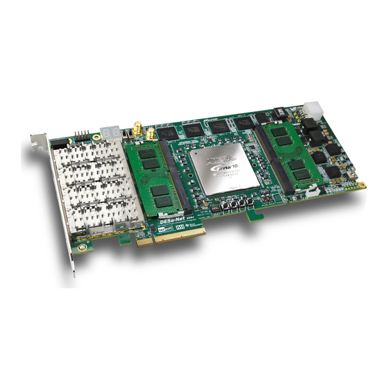
Board and installation guide. 1.1 General Description The Terasic DE5a-Net DDR4 Edition Arria 10 GX FPGA Development Kit provides the ideal hardware solution for designs that demand high capacity and bandwidth memory interfacing, ultra-low latency communication, and power efficiency. With a full-height,... -
Page 6: Key Features
Programmable clock generators Si5340A and Si5340B One SMA connector for external clock input One SMA connector for clock output Memory DDR4 SO-DIMM SDRAM QDRII+ SRAM FLASH DE5a-NET DDR4 www.terasic.com User Manual March 21, 2018... -
Page 7: Block Diagram
DE5a-Net board. To provide maximum flexibility for the users, all key components are connected with the Arria 10 GX FPGA device. Thus, users can configure the FPGA to implement any system design. DE5a-NET DDR4 www.terasic.com User Manual March 21, 2018... - Page 8 1,150K logic elements (LEs) 67-Mbits embedded memory 48 transceivers (12.5Gbps) 3,036 18-bit x 19-bit multipliers 1,518 Variable-precision DSP blocks 4 PCI Express hard IP blocks 768 user I/Os DE5a-NET DDR4 www.terasic.com User Manual March 21, 2018...
- Page 9 Up to 16GB DDR4 SO-DIMM SDRAM for each DDR4 socket 256MB FLASH General User I/O 8 user controllable LEDs 4 user push buttons 2 user slide switches 2 seven-segment displays On-Board Clock DE5a-NET DDR4 www.terasic.com User Manual March 21, 2018...
- Page 10 Edge connector for PC motherboard with x8 or x16 PCI Express slot Power Source PCI Express 6-pin DC 12V power PCI Express edge connector power Temperature Range FPGA: 0°C ~100°C DE5a-NET DDR4 www.terasic.com User Manual March 21, 2018...
-
Page 11: Operating Temperature - Important
It is therefore strongly recommended to use this board in an environment with sufficient airflow to dissipate the heat generated. It is also recommended to monitor the FPGA temperature continuously by adding Terasic IP introduced in chapter 5.1 in the project. -
Page 12: Chapter 2 Board Components
Users can refer to this figure for relative location of the connectors and key components. Figure 2-1 FPGA Board (Top) DE5a-NET DDR4 www.terasic.com User Manual March 21, 2018... -
Page 13: Configuration, Status And Setup
Launch Quartus Prime programmer and make sure the USB-Blaster II is detected. In Quartus Prime Programmer, add the configuration bit stream file (.sof), check the associated “Program/Configure” item, and click “Start” to start FPGA DE5a-NET DDR4 www.terasic.com User Manual March 21, 2018... - Page 14 The PCI Express Control DIP switch (SW5) is provided to enable or disable different configurations of the PCIe Connector. Table 2-2 lists the switch controls and description. Table 2-2 SW5 PCIe Control DIP Switch DE5a-NET DDR4 www.terasic.com User Manual March 21, 2018...
- Page 15 FPGA. Setting Position 4 of SW3 to “1” (down position) specifies the default factory image 2-4. Setting Position 4 of SW3 to “0” (up position) to be loaded, as shown in Figure DE5a-NET DDR4 www.terasic.com User Manual March 21, 2018...
-
Page 16: General User Input/Output
Figure 2-5 Position of DIP switch SW3 for Image Select – User Image Load 2.3 General User Input/Output This section describes the user I/O interface to the FPGA. User Defined Push-buttons DE5a-NET DDR4 www.terasic.com User Manual March 21, 2018... - Page 17 When a slide switch is in the DOWN position or the UPPER position, it provides a low logic level or a high logic level to the Arria 10 GX FPGA, respectively, as shown in Figure 2-6. DE5a-NET DDR4 www.terasic.com User Manual March 21, 2018...
- Page 18 A list of the pin names on the FPGA that are connected to the LEDs is given in Table 2-5. DE5a-NET DDR4 www.terasic.com User Manual March 21, 2018...
- Page 19 Each segment in a display is identified by an index listed from 0 to 6 with the positions given in Figure 2-8. In addition, the decimal point is identified as DP. Table 2-6 shows the mapping of the FPGA pin assignments to the 7-segment displays. DE5a-NET DDR4 www.terasic.com User Manual March 21, 2018...
- Page 20 PIN_AW8 segment signal OFF. HEX0 HEX0_D1 1.2-V PIN_AY8 HEX0 HEX0_D2 1.2-V PIN_AY9 HEX0 HEX0_D3 1.2-V PIN_BA9 HEX0 HEX0_D4 1.2-V PIN_BB9 HEX0 HEX0_D5 1.2-V PIN_BD10 HEX0 HEX0_D6 1.8-V PIN_V10 HEX0 HEX0_DP 1.8-V PIN_AG9 DE5a-NET DDR4 www.terasic.com User Manual March 21, 2018...
-
Page 21: Temperature Sensor And Fan Control
MAX6650, through an I2C interface, Users regulate and monitor the speed of fan depending on the measured system temperature. Figure2-10 shows the connection betweenthe Fan-Speed Regulator and Monitor and the Arria 10 GX FPGA. DE5a-NET DDR4 www.terasic.com User Manual March 21, 2018... - Page 22 1.2-V PIN_AY12 TEMP_OVERT_n SMBus alert (interrupt) 1.2-V PIN_AT14 TEMP_INT_n SMBus alert (interrupt) 1.2-V PIN_AU12 FAN_I2C_SCL 2-Wire Serial Clock 1.2-V PIN_AJ33 FAN_I2C_SDA 2-Wire Serial-Data 1.2-V PIN_AL32 Active-low AL FAN_ALERT_n 1.2-V PIN_AL31 ERT input DE5a-NET DDR4 www.terasic.com User Manual March 21, 2018...
-
Page 23: Power Monitor
Table 2-8 Pin Assignment of Power Monitor I2C bus Schematic Arria 10 GX Description I/O Standard Signal Name Pin Number POWER_MONITOR_I2C_SCL Power Monitor SCL 1.8V PIN_AT26 POWER_MONITOR_I2C_SDA Power Monitor SDA 1.8V PIN_AP25 POWER_MONITOR_ALERT Power Monitor ALERT 1.8V PIN_BD23 DE5a-NET DDR4 www.terasic.com User Manual March 21, 2018... -
Page 24: Clock Circuit
Table 2-9 lists the clock source, signal names, default frequency and their corresponding Arria 10 GX device pin numbers. Table 2-9 Clock Source, Signal Name, Default Frequency, Pin Assignments and Functions DE5a-NET DDR4 www.terasic.com User Manual March 21, 2018... - Page 25 B port QDRII+ reference QDRIIC_REFCLK_p 275 MHz LVDS PIN_G24 clock for C port QDRII+ reference QDRIID_REFCLK_p 275 MHz LVDS PIN_M34 clock for D port PCIe reference OB_PCIE_REFCLK_p 100 MHz LVDS PIN_AK40 clock DE5a-NET DDR4 www.terasic.com User Manual March 21, 2018...
-
Page 26: Flash Memory
This device is part of the shared flash and MAX (FM) bus, which connects to the flash memory and MAX V CPLD (5M2210) System Controller. Figure 2-13 shows the connections between the Flash, MAX and Arria 10 GX FPGA. DE5a-NET DDR4 www.terasic.com User Manual March 21, 2018... - Page 27 1.8-V PIN_J10 FLASH_A9 Address bus 1.8-V PIN_B17 FLASH_A10 Address bus 1.8-V PIN_J11 FLASH_A11 Address bus 1.8-V PIN_H8 FLASH_A12 Address bus 1.8-V PIN_A17 FLASH_A13 Address bus 1.8-V PIN_G8 FLASH_A14 Address bus 1.8-V PIN_G9 DE5a-NET DDR4 www.terasic.com User Manual March 21, 2018...
- Page 28 1.8-V PIN_K33 FLASH_D17 Data bus 1.8-V PIN_J39 FLASH_D18 Data bus 1.8-V PIN_AA32 FLASH_D19 Data bus 1.8-V PIN_J35 FLASH_D20 Data bus 1.8-V PIN_H36 FLASH_D21 Data bus 1.8-V PIN_AB32 FLASH_D22 Data bus 1.8-V PIN_J34 DE5a-NET DDR4 www.terasic.com User Manual March 21, 2018...
-
Page 29: Ddr4 So-Dimm
1200MHz memory clock for a maximum theoretical bandwidth up to153.6Gbps. Figure 2-14 shows the connections between the DDR4 SDRAM SO- DIMMs and Arria 10 GX FPGA. DE5a-NET DDR4 www.terasic.com User Manual March 21, 2018... - Page 30 DE5a-NET DDR4 www.terasic.com User Manual March 21, 2018...
- Page 31 Figure 2-14 Connection between the DDR4 and Arria 10 GX FPGA The pin assignments for DDR4 SDRAM SO-DIMM Bank-A and Bank-B are listed in Table 2-12 Table 2-13, in respectively. Table 2-12 DDR4-A Bank Pin Assignments, Schematic Signal Names, and Functions DE5a-NET DDR4 www.terasic.com User Manual March 21, 2018...
- Page 32 1.2-V POD PIN_AR39 DDR4A_DQ28 Data [28] 1.2-V POD PIN_AN38 DDR4A_DQ29 Data [29] 1.2-V POD PIN_AN37 DDR4A_DQ30 Data [30] 1.2-V POD PIN_AM38 DDR4A_DQ31 Data [31] 1.2-V POD PIN_AR37 DDR4A_DQ32 Data [32] 1.2-V POD PIN_AM30 DE5a-NET DDR4 www.terasic.com User Manual March 21, 2018...
- Page 33 DDR4A_DQ61 Data [61] 1.2-V POD PIN_AU27 DDR4A_DQ62 Data [62] 1.2-V POD PIN_AT29 DDR4A_DQ63 Data [63] 1.2-V POD PIN_AR27 DIFFERENTIAL 1.2-V DDR4A_DQS0 Data Strobe p[0] PIN_AK37 DIFFERENTIAL 1.2-V DDR4A_DQS_n0 Data Strobe n[0] PIN_AL37 DE5a-NET DDR4 www.terasic.com User Manual March 21, 2018...
- Page 34 Data Strobe n[7] PIN_AW30 Data Bus Inversion DDR4A_DBI_n0 1.2-V POD PIN_AK34 Data Bus Inversion 1.2-V POD DDR4A_DBI_n1 PIN_AP35 Data Bus Inversion 1.2-V POD DDR4A_DBI_n2 PIN_AT37 Data Bus Inversion 1.2-V POD DDR4A_DBI_n3 PIN_AP36 DE5a-NET DDR4 www.terasic.com User Manual March 21, 2018...
- Page 35 RAS_n DDR4A_BA0 Bank Select [0] SSTL-12 PIN_AR32 DDR4A_BA1 Bank Select [1] SSTL-12 PIN_AP33 Bank Group Select DDR4A_BG0 SSTL-12 PIN_AR33 Bank Group Select DDR4A_BG1 SSTL-12 PIN_AP33 DIFFERENTIAL 1.2-V DDR4A_CK0 Clock p0 PIN_BA34 SSTL DE5a-NET DDR4 www.terasic.com User Manual March 21, 2018...
- Page 36 DDR4A_REFCLK_p LVDS PIN_AV33 Reference Clock p DDR4 A port DDR4A_REFCLK_n LVDS PIN_AW33 Reference Clock n Table 2-13 DDR4-B Pin Assignments, Schematic Signal Names, and Functions Schematic Description I/O Standard Arria 10GX Pin DE5a-NET DDR4 www.terasic.com User Manual March 21, 2018...
- Page 37 1.2-V POD PIN_AP11 DDR4B_DQ29 Data [29] 1.2-V POD PIN_AN11 DDR4B_DQ30 Data [30] 1.2-V POD PIN_AR11 DDR4B_DQ31 Data [31] 1.2-V POD PIN_AR7 DDR4B_DQ32 Data [32] 1.2-V POD PIN_AU8 DDR4B_DQ33 Data [33] 1.2-V POD PIN_AU9 DE5a-NET DDR4 www.terasic.com User Manual March 21, 2018...
- Page 38 Data [62] 1.2-V POD PIN_AB13 DDR4B_DQ63 Data [63] 1.2-V POD PIN_AD13 DIFFERENTIAL 1.2-V DDR4B_DQS0 Data Strobe p[0] PIN_AV18 DIFFERENTIAL 1.2-V DDR4B_DQS_n0 Data Strobe n[0] PIN_AU18 DDR4B_DQS1 Data Strobe p[1] DIFFERENTIAL 1.2-V PIN_BA15 DE5a-NET DDR4 www.terasic.com User Manual March 21, 2018...
- Page 39 DDR4B_DBI_n0 1.2-V POD PIN_AT19 Data Bus Inversion 1.2-V POD DDR4B_DBI_n1 PIN_AY18 Data Bus Inversion 1.2-V POD DDR4B_DBI_n2 PIN_BC17 Data Bus Inversion 1.2-V POD DDR4B_DBI_n3 PIN_AT11 DDR4B_DBI_n4 Data Bus Inversion 1.2-V POD PIN_AN10 DE5a-NET DDR4 www.terasic.com User Manual March 21, 2018...
- Page 40 PIN_AU14 DDR4B_BA1 Bank Select [1] SSTL-12 PIN_AP13 Bank Group Select DDR4B_BG0 SSTL-12 PIN_AR13 Bank Group Select DDR4B_BG1 SSTL-12 PIN_BB14 DIFFERENTIAL 1.2-V DDR4B_CK0 Clock p0 PIN_BA10 SSTL DDR4B_CK_n0 Clock n0 DIFFERENTIAL 1.2-V PIN_BB10 DE5a-NET DDR4 www.terasic.com User Manual March 21, 2018...
- Page 41 DDR4B_SDA 1.2 V PIN_AP9 Clock Chip I2C Serial DDR4B_SCL 1.2 V PIN_AP16 Data Bus DDR4 A port DDR4B_REFCLK_p LVDS PIN_AP14 Reference Clock p DDR4 A port DDR4B_REFCLK_n LVDS PIN_AR14 Reference Clock n DE5a-NET DDR4 www.terasic.com User Manual March 21, 2018...
-
Page 42: Qdrii+ Sram
QDRIIA_A15 Address bus[15] 1.8-V HSTL Class I PIN_L7 QDRIIA_A16 Address bus[16] 1.8-V HSTL Class I PIN_K7 QDRIIA_A17 Address bus[17] 1.8-V HSTL Class I PIN_K8 QDRIIA_A18 Address bus[18] 1.8-V HSTL Class I PIN_J9 DE5a-NET DDR4 www.terasic.com User Manual March 21, 2018... - Page 43 1.8-V HSTL Class I PIN_H11 QDRIIA_Q11 Read Data bus[11] 1.8-V HSTL Class I PIN_J14 QDRIIA_Q12 Read Data bus[12] 1.8-V HSTL Class I PIN_K14 QDRIIA_Q13 Read Data bus[13] 1.8-V HSTL Class I PIN_K13 DE5a-NET DDR4 www.terasic.com User Manual March 21, 2018...
- Page 44 QDRIIB_A7 Address bus[7] 1.8-V HSTL Class I PIN_C15 QDRIIB_A8 Address bus[8] 1.8-V HSTL Class I PIN_F15 QDRIIB_A9 Address bus[9] 1.8-V HSTL Class I PIN_F16 QDRIIB_A10 Address bus[10] 1.8-V HSTL Class I PIN_H15 DE5a-NET DDR4 www.terasic.com User Manual March 21, 2018...
- Page 45 1.8-V HSTL Class I PIN_J23 QDRIIB_Q3 Read Data bus[3] 1.8-V HSTL Class I PIN_H23 QDRIIB_Q4 Read Data bus[4] 1.8-V HSTL Class I PIN_H21 QDRIIB_Q5 Read Data bus[5] 1.8-V HSTL Class I PIN_H22 DE5a-NET DDR4 www.terasic.com User Manual March 21, 2018...
- Page 46 Table 2-16 QDRII+ SRAM C Pin Assignments, Schematic Signal Names, and Functions Schematic Arria 10 GX Pin Description I/O Standard Signal Name Number QDRIIC_A0 Address bus[0] 1.8-V HSTL Class I PIN_D25 QDRIIC_A1 Address bus[1] 1.8-V HSTL Class I PIN_D26 DE5a-NET DDR4 www.terasic.com User Manual March 21, 2018...
- Page 47 1.8-V HSTL Class I PIN_AD34 QDRIIC_D12 Write data bus[12] 1.8-V HSTL Class I PIN_AE34 QDRIIC_D13 Write data bus[13] 1.8-V HSTL Class I PIN_AE33 QDRIIC_D14 Write data bus[14] 1.8-V HSTL Class I PIN_AE32 DE5a-NET DDR4 www.terasic.com User Manual March 21, 2018...
- Page 48 1.8-V HSTL Class I PIN_F26 Write Port Select QDRIIC_DOFF_n PLL Turn Off 1.8-V HSTL Class I PIN_D24 On-Die Termination QDRIIC_ODT 1.8-V HSTL Class I PIN_B25 Input QDRIIC_QVLD Valid Output Indicator 1.8-V HSTL Class I PIN_U34 DE5a-NET DDR4 www.terasic.com User Manual March 21, 2018...
- Page 49 1.8-V HSTL Class I PIN_F36 QDRIID_D4 Write data bus[4] 1.8-V HSTL Class I PIN_D33 QDRIID_D5 Write data bus[5] 1.8-V HSTL Class I PIN_F31 QDRIID_D6 Write data bus[6] 1.8-V HSTL Class I PIN_G30 DE5a-NET DDR4 www.terasic.com User Manual March 21, 2018...
- Page 50 1.8-V HSTL Class I PIN_F30 QDRIID_BWS_n1 Byte Write select[1] 1.8-V HSTL Class I PIN_E31 Differential 1.8-V QDRIID_K_p PIN_F32 Clock P HSTL Class I Differential 1.8-V QDRIID_K_n PIN_E32 Clock N HSTL Class I DE5a-NET DDR4 www.terasic.com User Manual March 21, 2018...
-
Page 51: Qspf+ Ports
QSFP+ and Arria 10 GX FPGA. Figure 2-15 Connection between the QSFP+ and Arria GX FPGA Table 2-18, Table 2-19, Table 2-20 Table 2-21 list the QSFP+ A, B, C and D pin DE5a-NET DDR4 www.terasic.com User Manual March 21, 2018... - Page 52 PIN_AG10 Table 2-19 QSFP+ B Pin Assignments, Schematic Signal Names, and Functions Schematic Arria 10 GX Description I/O Standard Signal Name Pin Number QSFPB_TX_P0 Transmitter data of channel 0 1.4-V PCML PIN_AP1 DE5a-NET DDR4 www.terasic.com User Manual March 21, 2018...
- Page 53 Transmitter data of channel 0 1.4-V PCML PIN_AB1 QSFPC_TX_N0 Transmitter data of channel 0 1.4-V PCML PIN_AB2 QSFPC_RX_P0 Receiver data of channel 0 1.4-V PCML PIN_AA3 QSFPC_RX_N0 Receiver data of channel 0 1.4-V PCML PIN_AA4 DE5a-NET DDR4 www.terasic.com User Manual March 21, 2018...
- Page 54 Receiver data of channel 1 1.4-V PCML PIN_G3 QSFPD_RX_N1 Receiver data of channel 1 1.4-V PCML PIN_G4 QSFPD_TX_P2 Transmitter data of channel 2 1.4-V PCML PIN_F1 QSFPD_TX_N2 Transmitter data of channel 2 1.4-V PCML PIN_F2 DE5a-NET DDR4 www.terasic.com User Manual March 21, 2018...
-
Page 55: Pci Express
The PCIE_REFCLK_p signal is a differential input that is driven from the PC motherboard on this board through the PCIe edge connector. A DIP switch (SW5) is connected to the PCI Express to allow different configurations to enable a x1, x4, or x8 PCIe. DE5a-NET DDR4 www.terasic.com User Manual March 21, 2018... - Page 56 PCIE_TX_n5 Add-in card transmit bus 1.4-V PCML PIN_AH43 PCIE_TX_p6 Add-in card transmit bus 1.4-V PCML PIN_AF44 PCIE_TX_n6 Add-in card transmit bus 1.4-V PCML PIN_AF43 PCIE_TX_p7 Add-in card transmit bus 1.4-V PCML PIN_AD44 DE5a-NET DDR4 www.terasic.com User Manual March 21, 2018...
- Page 57 Hot plug detect x1 PCIe slot PCIE_PRSNT2n_x1 enabled using SW5 dip switch Hot plug detect x4 PCIe slot PCIE_PRSNT2n_x4 enabled using SW5 dip switch Hot plug detect x8 PCIe slot PCIE_PRSNT2n_x8 enabled using SW5 dip switch DE5a-NET DDR4 www.terasic.com User Manual March 21, 2018...
-
Page 58: Expansion Header
2-12 RS-422 Expansion Header The 2x5 RS-422 expansion header is designed to perform communication between boards. Users can use Terasic defined RS422-RJ45 board to translate RS-422 signal, allowing a transmission speed of up to 26 Mbps. Figure 2-17 shows the RS-422 application diagram. - Page 59 DE5a-NET DDR4 www.terasic.com User Manual March 21, 2018...
-
Page 60: Chapter 3 System Builder
Board damaged for wrong pin/bank voltage assignment. Board malfunction caused by wrong device connections or missing pin counts for connected ends. Performance dropped because of improper pin assignments DE5a-NET DDR4 www.terasic.com User Manual March 21, 2018... - Page 61 DE5a-NET DDR4 www.terasic.com User Manual March 21, 2018...
-
Page 62: General Design Flow
The Quartus Prime setting file contains information such as FPGA device type, top-level pin assignment, and I/O standard for each user-defined I/O pin. Finally, Quartus Prime programmer must be used to download SOF file to the FPGA board using JTAG interface. DE5a-NET DDR4 www.terasic.com User Manual March 21, 2018... -
Page 63: Using System Builder
Figure 3-2 The System Builder window Enter Project Name The project name entered in the circled area as shown in Figure 3-3, will be assigned automatically as the name of the top-level design entry. DE5a-NET DDR4 www.terasic.com User Manual March 21, 2018... - Page 64 Quartus project or it would result in compilation error. Hence please do not select them if they are not needed in the design. To use the DDR4 controller, please refer to the DDR4 SDRAM demonstration in Chapter 6. DE5a-NET DDR4 www.terasic.com User Manual March 21, 2018...
- Page 65 Note: If users need to dynamically change the frequency, they would need to modify the generated control code themselves. DE5a-NET DDR4 www.terasic.com User Manual March 21, 2018...
- Page 66 The System Builder also provides functions to restore default setting, load a setting, and save board configuration file, as shown in Figure 3-6. Users can save the current board configuration information into a .cfg file and load it into the System Builder. DE5a-NET DDR4 www.terasic.com User Manual March 21, 2018...
- Page 67 Top Level Verilog File for Quartus Prime Si5340_controller (*) Si5340A and Si5340BExternal Oscillator Controller IP <Project name>.qpf Quartus Prime Project File <Project name>.qsf Quartus Prime Setting File <Project name>.sdc Synopsis Design Constraints File for Quartus Prime DE5a-NET DDR4 www.terasic.com User Manual March 21, 2018...
- Page 68 For Si5340A, its controller will be instantiated in the Quartus Prime top-level file, as listed below: For Si5340B, its controller will be instantiated in the Quartus Prime top-level file, as listed below: DE5a-NET DDR4 www.terasic.com User Manual March 21, 2018...
-
Page 69: Chapter 4 Flash Programming
Programmer Tool to program the common flash interface (CFI) flash memory device on the FPGA board. The Arria X GX FPGA development board ships with the CFI flash device preprogrammed with a default factory FPGA configuration for running the Parallel Flash Loader design example. DE5a-NET DDR4 www.terasic.com User Manual March 21, 2018... -
Page 70: Cfi Flash Memory Map
Please make sure the FPGA configuration data has been stored in the CFI flash. Set the FPGA configuration mode to FPPx32 mode by setting SW3 MSEL[0:2] as 000 as shown in Figure 4-1. DE5a-NET DDR4 www.terasic.com User Manual March 21, 2018... -
Page 71: Flash Programming With Users Design
FPGA on power up. For convenience, the translation and programming batch files are available on the following folder in the System CD. Demonstrations/Hello/flash_programming_batch There folder contains five files as shown in Table 4-2 DE5a-NET DDR4 www.terasic.com User Manual March 21, 2018... - Page 72 If your design includes a NIOS II processor and the NIOS II program is stored on external memory, users must to perform following items so the NIOS II program can be boot from flash successfully: DE5a-NET DDR4 www.terasic.com User Manual March 21, 2018...
-
Page 73: Restore Factory Settings
FPGA development board. Perform the following instructions: Make sure the Nios II EDS and USB-Blaster II driver are installed. Make sure the FPGA board and PC are connected with an UBS Cable. Power on the FPGA board. DE5a-NET DDR4 www.terasic.com User Manual March 21, 2018... - Page 74 Flasher Loader design in the FPGA. The Parallel Flash Loader design is included in the default code PFL and the source code is available in the folder Demonstrations/ PFL in System CD. DE5a-NET DDR4 www.terasic.com User Manual March 21, 2018...
-
Page 75: Chapter 5 Peripheral Reference Design
System CD. 5.1 Temperature Monitor: Board Protection This section introduces a Terasic Temperature Monitor IP which can be used to monitor board temperature and raise an alert when the FPGA temperature reaches the specified threshold. - Page 76 Set alter temperature in degree C. Alert_Temperature[9:0] input Typically 80 is recommended. Do NOT exceed 95. High active. When FPGA temperature Alert output exceeds the threshold specified by Alert_temperature, the alert pin will be DE5a-NET DDR4 www.terasic.com User Manual March 21, 2018...
- Page 77 If the FPGA temperature exceed 80s degree, the LEDs will stop blinking. For test, please modify the Alert_Temperature to a lower value to so the measured temperature value can exceed the temperature specified by .Alert_Temperature the in finally. DE5a-NET DDR4 www.terasic.com User Manual March 21, 2018...
-
Page 78: Configure Si5340A/B In Rtl
Si5340 corresponding output channels will become available and users can select desired frequencies. For example, when checking QSFP+ A box (See Figure 5-3), SI5340A QSFPA_REFCLK_P/N can provide seven frequencies from 100Mhz to 644.5312Mhz for users selecting. DE5a-NET DDR4 www.terasic.com User Manual March 21, 2018... - Page 79 Figure 5-4 Enable Si5340A and Si5340BB clock on System Builder Click "Generate" button, then, open the Quartus Project generated by System Builder, the control IPs for Si5340A and Si5340B can be found in the top level file. DE5a-NET DDR4 www.terasic.com User Manual March 21, 2018...
- Page 80 User Logic and compile it, and then, Si5340 can output desired frequencies. At the same time, System Builder will set Clock constrain according user’s preset frequency in a SDC file DE5a-NET DDR4 www.terasic.com User Manual March 21, 2018...
- Page 81 (0: Module Reset, 1: Normal) Start to Configure(positive edge iStart input trigger) Setting Si5340 Output Channel iPLL_OUTX_FREQ_SEL input Frequency Value Si5340 Configuration status oPLL_REG_CONFIG_DONE output ( 0: Configuration in Progress, 1: Configuration Complete) DE5a-NET DDR4 www.terasic.com User Manual March 21, 2018...
- Page 82 Power Down 3'b001 644.53125 3'b010 322.26 3'b011 312.25 3'b100 3'b101 156.25 3'b110 3'b111 Table 5-4 Si5340B Controller Reference Clock Frequency Setting iPLL_OUT_FRE DDR4 QDRII PCIE Q_SEL MODE Frequency(MHz) Frequency(MHz) Frequency(MHz) Setting 5'b00000 DE5a-NET DDR4 www.terasic.com User Manual March 21, 2018...
- Page 83 Silicon Labs. This tool can help users to set the Si5340’s output frequency of each channel through the GUI interface, and it will automatically calculate the Register parameters required for each frequency. The tool download link: http://www.silabs.com/products/clocksoscillators/pages/timing-software- development-tools.aspx DE5a-NET DDR4 www.terasic.com User Manual March 21, 2018...
- Page 84 Figure 5-6 ClockBuilder Pro Wizard After the installation, select Si5340, and configure the input frequency and output frequency as shown in Figure 5-7. Figure Define Output Clock DE5a-NET DDR4 www.terasic.com User Manual March 21, 2018...
- Page 85 Figure 5-8 Open Design Report on ClockBuilder Pro Wizard Open Si5340 control IP sub-module “si5340a_i2c_reg_controller.v “ as shown in Figure 5-9, refer Design Report parameter to modify sub-module corresponding register value (See Figure 5-10). DE5a-NET DDR4 www.terasic.com User Manual March 21, 2018...
- Page 86 1. No need to modify all Design Report parameters in si5340a_i2c_reg_controller.v/si5340b_i2c_reg_controller.v, users can ignore parameters which have nothing to do with the frequency setting 2. After the manually modifying, please remember to modify clock constrain setting in .SDC file DE5a-NET DDR4 www.terasic.com User Manual March 21, 2018...
-
Page 87: Nios Ii Control For Si5340/Temperature/Power
The I2C pins from chip are connected to Qsys System Interconnect Fabric through PIO controllers. The Nios II program toggles the PIO controller to implement the I2C protocol. The Nios II program is running in the on-chip memory. DE5a-NET DDR4 www.terasic.com User Manual March 21, 2018... - Page 88 With the menu, users can perform the test for the temperatures sensor, external PLL and power monitor. Note, pressing ‘ENTER’ should be followed with the choice number. Figure 5-12 Menu of Demo Program DE5a-NET DDR4 www.terasic.com User Manual March 21, 2018...
- Page 89 In the external PLL programming test, the program will program the PLL first, and subsequently will use TERASIC QSYS custom CLOCK_COUNTER IP to count the clock count in a specified period to check whether the output frequency is changed as configured.
- Page 90 For programmable PLL Si5340B test, please input key ‘3’ and press ‘Enter’ in the nios-terminal first, then select the desired output frequency of DDR4/PCIE/QDRII REFCLK, as shown in Figure 5-16. Figure 5-13 Temperature Demo DE5a-NET DDR4 www.terasic.com User Manual March 21, 2018...
- Page 91 Figure 5-14 power monitor Demo DE5a-NET DDR4 www.terasic.com User Manual March 21, 2018...
-
Page 92: Fan Speed Control
I2C_Config I2C_Bus_Controller set and monitor the RPM of the fansink, respectively. A pre-scaler is used as frequency divider for the clock frequency of I2C. Users need to calculate the DE5a-NET DDR4 www.terasic.com User Manual March 21, 2018... - Page 93 The status of BIT 4 ~ 7 can be ignored because BIT 4 is for MAX6651 only and BIT 5 ~ 7 are always low. Table 5-5 POR(DEFAULT)S NAME FUNCTION Alarm-Enable TATE DE5a-NET DDR4 www.terasic.com User Manual March 21, 2018...
- Page 94 Demonstration Setup Make sure Quartus Prime is installed on the host PC. Connect the DE5a-Net and the host PC via USB cable. Install the USB-Blaster II driver if necessary. DE5a-NET DDR4 www.terasic.com User Manual March 21, 2018...
- Page 95 Execute the demo batch file “test_ub2.bat” under the batch file folder \Fan\demo_batch. When SW[0] is set to 0, the RPM would slowly be adjusted to ~2000. When SW[0] is set to 1, the RPM would slowly be adjusted to ~5000. DE5a-NET DDR4 www.terasic.com User Manual March 21, 2018...
-
Page 96: Chapter 6 Memory Reference Design
The memory architecture features separate read and write ports operating twice per clock cycle to deliver a total of four data transfers per cycle. The resulting performance increase is particularly valuable in bandwidth-intensive and low- latency applications. DE5a-NET DDR4 www.terasic.com User Manual March 21, 2018... - Page 97 The four QDRII+ SRAM controllers are configured as a 72Mb controller. The QDRII+ SRAM IP generates a 550MHz clock as memory clock and a half-rate system clock, 275MHz, for the controllers. DE5a-NET DDR4 www.terasic.com User Manual March 21, 2018...
- Page 98 Quartus Prime 16.1.2 Standard Edition Demonstration Source Code Project directory: QDRII_x4_Test_550MHz Bit stream used: DE5A_NET_DDR4.sof Demonstration Batch File Demo Batch File Folder: QDRII_x4_Test_550MHz\demo_batch The demo batch files include the followings: DE5a-NET DDR4 www.terasic.com User Manual March 21, 2018...
-
Page 99: Ddr4 Sdram Test
This demonstration performs a memory test function on the two DDR4-SDRAM SO-DIMM on the DE5a-Net. The memory size of each DDR4 SDRAM SO-DIMM used in this test is 4 GB. Function Block Diagram DE5a-NET DDR4 www.terasic.com User Manual March 21, 2018... - Page 100 2. Setup correct parameters in the dialog of DDR4 controller. Design Tools Quartus Prime 16.1.2 Standard Edition Demonstration Source Code Project Directory: Demonstration\RTL_DDR4_4GB_x2 Bit Stream: DE5A_NET_DDR4_4GB.sof Demonstration Batch File DE5a-NET DDR4 www.terasic.com User Manual March 21, 2018...
- Page 101 Press BUTTON0 again to regenerate the test control signals for a repeat test. Table 6-2 LED Indicators NAME Description LED0 Reset LED1 DDR4 (A) test result LED2 DDR4 (B) test result LED3 50MHz clock source DE5a-NET DDR4 www.terasic.com User Manual March 21, 2018...
-
Page 102: Ddr4 Sdram Test By Nios Ii
II processor is used to perform memory test. The Nios II program is running in the On- Chip Memory. A PIO Controller is used to monitor buttons status which is used to trigger starting memory testing. DE5a-NET DDR4 www.terasic.com User Manual March 21, 2018... - Page 103 Prime 16.1.2 Standard Edition Nios II Software Build Tools for Eclipse 16.1 Demonstration Source Code Quartus Project directory: Nios_DDR4_X2 Nios II Eclipse: NIOS_DDR4_X2\software Nios II Project Compilation DE5a-NET DDR4 www.terasic.com User Manual March 21, 2018...
- Page 104 Press Button3~Button0 of the FPGA board to start SDRAM verify process. Press Button0 for continued test. The program will display progressing and result information, as shown in Figure 6-4. DE5a-NET DDR4 www.terasic.com User Manual March 21, 2018...
- Page 105 Figure 6-4 Progress and Result Information for the DDR4 Demonstration DE5a-NET DDR4 www.terasic.com User Manual March 21, 2018...
-
Page 106: Chapter 7 Memory Reference Design
FPGA System and PC System. The FPGA System is developed based on Arria 10 Hard IP for PCI Express with Avalon-MM DMA. The application software on the PC side is developed by Terasic based on Altera’s PCIe kernel mode driver. -
Page 107: Pc Pci Express Software Sdk
(DID) is 0xE003. If different VID and DID are used in the design, users need to modify the PCIe vendor ID (VID) and device ID (DID) in the driver INF file accordingly. Express Library implemented single named DE5a-NET DDR4 www.terasic.com User Manual March 21, 2018... -
Page 108: Pci Express Software Stack
Windows. The PCIe library module TERASIC_PCIE_AVMM.dll provides DMA and direct I/O access for user application program to communicate with FPGA. Users can develop their applications based on this DLL. The altera_pcie_win_driver.sys kernel driver is provided by Altera. DE5a-NET DDR4 www.terasic.com User Manual March 21, 2018... - Page 109 1. Install the DE5a-Net on the PCIe slot of the host PC 2. Make sure Altera Programmer and USB-Blaster II driver are installed 3. Execute test.bat in "CDROM\Demonstrations\PCIe_Fundamental\demo_batch" to configure the FPGA DE5a-NET DDR4 www.terasic.com User Manual March 21, 2018...
- Page 110 Figure 7-3 Screenshot of launching Update Driver Software… dialog 6. In the How do you want to search for driver software dialog, click Browse my computer for driver software item, as shown in Figure 7-4 DE5a-NET DDR4 www.terasic.com User Manual March 21, 2018...
- Page 111 Figure 7-5. Click the Next button. Figure 7-5 Browse for driver software on your computer 8. When the Windows Security dialog appears, as shown Figure 7-6, click the Install button. DE5a-NET DDR4 www.terasic.com User Manual March 21, 2018...
- Page 112 Figure 7-7 Click Close when the installation of Altera PCI API Driver is complete 10. Once the driver is successfully installed, users can see the Altera PCI API Driver under the device manager window, as shown in Figure7-8. DE5a-NET DDR4 www.terasic.com User Manual March 21, 2018...
- Page 113 Copy TERASIC_PCIE_AVMM.DLL to the folder where the project.exe is located. Dynamically load TERASIC_PCIE_AVMM.DLL in C/C++ program. To load the DLL, please refer to the PCIe fundamental example below. Call the SDK API to implement the desired application. DE5a-NET DDR4 www.terasic.com User Manual March 21, 2018...
-
Page 114: Pci Express Library Api
A value zero means failed to connect the target PCIe card. This handle value is used as a parameter for other functions, e.g. PCIE_Read32. Users need to call PCIE_Close to release handle once the handle is no more used. PCIE_Close Function: DE5a-NET DDR4 www.terasic.com User Manual March 21, 2018... - Page 115 A buffer to retrieve the 32-bit data. Return Value: Return true if read data is successful; otherwise false is returned. PCIE_Write32 Function: Write a 32-bit data to the FPGA Board. Prototype: bool PCIE_Write32( DE5a-NET DDR4 www.terasic.com User Manual March 21, 2018...
- Page 116 Specify the target BAR. PcieAddress: Specify the target address in FPGA. pByte: A buffer to retrieve the 8-bit data. Return Value: Return true if read data is successful; otherwise false is returned. DE5a-NET DDR4 www.terasic.com User Manual March 21, 2018...
- Page 117 PCIE_DmaRead Function: Read data from the memory-mapped memory of FPGA board in DMA. Maximal read size is (4GB-1) bytes. Prototype: bool PCIE_DmaRead( PCIE_HANDLE hPCIE, PCIE_LOCAL_ADDRESS LocalAddress, void *pBuffer, uint32_t dwBufSize Parameters: hPCIE: DE5a-NET DDR4 www.terasic.com User Manual March 21, 2018...
- Page 118 A pointer to a memory buffer to store the data which will be written to FPGA. dwDataSize: Specify the byte number of data which will be written to FPGA. Return Value: Return true if write data is successful; otherwise false is returned. PCIE_ConfigRead32 Function: DE5a-NET DDR4 www.terasic.com User Manual March 21, 2018...
-
Page 119: Pcie Reference Design - Fundamental
The demo file is located in the batch folder: CDROM\Demonstrations\PCIe_Fundamental\demo_batch The folder includes following files: FPGA Configuration File: DE5A_NET.sof Download Batch file: test.bat Windows Application Software folder : windows_app, includes DE5a-NET DDR4 www.terasic.com User Manual March 21, 2018... - Page 120 3. Install PCIe driver if necessary. The driver is located in the folder: CDROM\Demonstration\PCIe_SW_KIT\Windows\PCIe_Driver. 4. Restart Windows 5. Make sure the Windows has detected the FPGA Board by checking the Windows Control panel as shown in Figure 7-10. DE5a-NET DDR4 www.terasic.com User Manual March 21, 2018...
- Page 121 6. Goto windows_app folder, execute PCIE_FUNDMENTAL.exe. A menu will appear as shown in Figure 7-11. Figure 7-11 Screenshot of Program Menu 7. Type 0 followed by a ENTERY key to select Led Control item, then input 15 (hex 0x0f) DE5a-NET DDR4 www.terasic.com User Manual March 21, 2018...
- Page 122 Figure 7-13 Screenshot of Button Status Report 9. Type 2 followed by an ENTERY key to select DMA Testing item. The DMA test result will be report as shown in Figure 7-14. DE5a-NET DDR4 www.terasic.com User Manual March 21, 2018...
- Page 123 LED and monitor the Button Status, and the On-Chip memory is used for performing DMA testing. The PIO controllers and the On-Chip memory are connected to the PCI Express Hard IP controller through the Memory-Mapped Interface. DE5a-NET DDR4 www.terasic.com User Manual March 21, 2018...
- Page 124 Implement dynamically load for TERAISC_PCIE_AVMM.DLL PCIE.h TERASIC_PCIE_AVMM.h SDK library file, defines constant and data structure The main program PCIE_FUNDAMENTAL.cpp includes the header file "PCIE.h" and defines the controller address according to the FPGA design. DE5a-NET DDR4 www.terasic.com User Manual March 21, 2018...
- Page 125 The LED control is implemented by calling PCIE_Write32 API, as shown below: The button status query is implemented by calling the PCIE_Read32 API, as shown below: The memory-mapped memory read and write test is implemented by PCIE_DmaWrite and PCIE_DmaRead API, as shown below: DE5a-NET DDR4 www.terasic.com User Manual March 21, 2018...
- Page 126 DE5a-NET DDR4 www.terasic.com User Manual March 21, 2018...
-
Page 127: Pcie Reference Design - Ddr4
5. Restart Windows 6. Make sure the Windows has detected the FPGA Board by checking the Windows Control panel. 7. Goto windows_app folder, execute PCIE_DDR4.exe. A menu will appear as shown in Figure 7-16. DE5a-NET DDR4 www.terasic.com User Manual March 21, 2018... - Page 128 Figure 7-17 Screenshot of Link Info 9. Type 3 followed by an ENTERY key to select DMA On-Chip Memory Test item. The DMA write and read test result will be report as shown in Figure 7-18. DE5a-NET DDR4 www.terasic.com User Manual March 21, 2018...
- Page 129 Figure 7-19 Screenshot of DDR4-A SOSIMM Memory DAM Test Result 11. Type 5 followed by an ENTERY key to select DMA DDR4-B SODIMM Memory Test item. The DMA write and read test result will be report as shown in Figure 7-20. DE5a-NET DDR4 www.terasic.com User Manual March 21, 2018...
- Page 130 LED and monitor the Button Status, and the On-Chip memory is used for performing DMA testing. The PIO controllers and the On-Chip memory are connected to the PCI Express Hard IP controller through the Memory-Mapped Interface. DE5a-NET DDR4 www.terasic.com User Manual March 21, 2018...
- Page 131 Implement dynamically load for TERAISC_PCIE_AVMM.DLL PCIE.h TERASIC_PCIE_AVMM.h SDK library file, defines constant and data structure The main program PCIE_DDR4.cpp includes the header file "PCIE.h" and defines the controller address according to the FPGA design. DE5a-NET DDR4 www.terasic.com User Manual March 21, 2018...
- Page 132 The LED control is implemented by calling PCIE_Write32 API, as shown below: The button status query is implemented by calling the PCIE_Read32 API, as shown below: The memory-mapped memory read and write test is implemented by PCIE_DmaWrite DE5a-NET DDR4 www.terasic.com User Manual March 21, 2018...
- Page 133 PCIE_DmaRead API, as shown below: The PCIe link information is implemented by PCIE_ConfigRead32 API, as shown below: DE5a-NET DDR4 www.terasic.com User Manual March 21, 2018...
-
Page 134: Chapter 8 Pci Express Reference Design For Linux
FPGA System and PC System. The FPGA System is developed based on Arria 10 Hard IP for PCI Express with Avalon-MM DMA. The application software on the PC side is developed by Terasic based on Altera’s PCIe kernel mode driver. -
Page 135: User Manual March 21, 2018
PCIe vendor ID (VID) and device ID (DID) in the driver project and rebuild the driver. The ID is defined in the file PCIe_SW_KIT/Linux/PCIe_Driver/altera_pcie_cmd.h. The PCI Express Library is implemented as a single .so file named terasic_pcie_qsys.so. DE5a-NET DDR4 www.terasic.com User Manual March 21, 2018... -
Page 136: Pci Express Software Stack
Linux. The PCIe library module terasic_pcie_qys.so provides DMA and direct I/O access for user application program to communicate with FPGA. Users can develop their applications based on this .so library file. The altera_pcie.ko kernel driver is provided by Altera. DE5a-NET DDR4 www.terasic.com User Manual March 21, 2018... - Page 137 7. Type the following commands to compile and install the driver altera_pcie.ko, and make sure driver is loaded successfully and FPGA is detected by the driver as shown in Figure 8-3. make sudo sh load_driver DE5a-NET DDR4 www.terasic.com User Manual March 21, 2018...
- Page 138 PCIe fundamental example below. Call the library API to implement the desired application. Users can easily communicate with the FPGA through the PCIe bus through the terasic_pcie_qsys.so API. The details of API are described below: DE5a-NET DDR4 www.terasic.com User Manual March 21, 2018...
-
Page 139: Pci Express Library Api
Download Batch file: test.sh Linux Application Software folder : linux_app, includes PCIE_FUNDAMENTAL terasic_pcie_qsys.so Demonstration Setup 1. Install the FPGA board on your PC as shown in Figure8-4. DE5a-NET DDR4 www.terasic.com User Manual March 21, 2018... - Page 140 FPGA board is detected, developers can find the /dev/altera_pcieX(where X is 0~255) in Linux file system as shown below. 8. Goto linux_app folder, execute PCIE_FUNDMENTAL. A menu will appear as shown in Figure 8-5. DE5a-NET DDR4 www.terasic.com User Manual March 21, 2018...
- Page 141 8-6. If input 0 (hex 0x00), all led will be turn off. Figure 8-6 Screenshot of LED Control 10. Type 1 followed by an ENTERY key to select Button Status Read item. The button DE5a-NET DDR4 www.terasic.com User Manual March 21, 2018...
- Page 142 Figure 8-8. Figure 8-8 Screenshot of DMA Memory Test Result 12. Type 99 followed by an ENTERY key to exit this test program Development Tools Quartus Prime 16.1.2 Standard Edition DE5a-NET DDR4 www.terasic.com User Manual March 21, 2018...
- Page 143 Figure 8-9 Hardware block diagram of the PCIe reference design Linux Based Application Software Design The application software project is built by GNU Toolchain. The project includes the following major files: DE5a-NET DDR4 www.terasic.com User Manual March 21, 2018...
- Page 144 The FPGA is configured with the associated bit-stream file and the host is rebooted. The PCI express driver is loaded successfully. The LED control is implemented by calling PCIE_Write32 API, as shown below: DE5a-NET DDR4 www.terasic.com User Manual March 21, 2018...
-
Page 145: Pcie Reference Design - Ddr4
The demo file is located in the batch folder: CDROM/Demonstrations/PCIe_DDR4/demo_batch The folder includes following files: FPGA Configuration File: DE5A_NET.sof Download Batch file: test.sh Linux Application Software folder : linux_app, includes PCIE_DDR4 terasic_pcie_qsys.so Demonstration Setup DE5a-NET DDR4 www.terasic.com User Manual March 21, 2018... - Page 146 10. Type 2 followed by an ENTERY key to select Link Info item. The PCIe link information will be shown as in Figure 8-11. Gen3 link speed and x8 link width are expected. DE5a-NET DDR4 www.terasic.com User Manual March 21, 2018...
- Page 147 Figure 8-12 Screenshot of On-Chip Memory DMA Test Result 12. Type 4 followed by an ENTERY key to select DMA DDR4-A SODIMM Memory Test item. The DMA write and read test result will be report as shown in Figure 8-14. DE5a-NET DDR4 www.terasic.com User Manual March 21, 2018...
- Page 148 The DMA write and read test result will be report as shown in Figure 8-15. Figure 8-15 Screenshot of DDR4-B SOSIMM Memory DAM Test Result 14. Type 99 followed by an ENTERY key to exit this test program. DE5a-NET DDR4 www.terasic.com User Manual March 21, 2018...
- Page 149 DMA testing. The PIO controllers and the On-Chip memory are connected to the PCI Express Hard IP controller through the Memory-Mapped Interface. Figure 8-16 Hardware block diagram of the PCIe_DDR4 reference design Linux Based Application Software Design DE5a-NET DDR4 www.terasic.com User Manual March 21, 2018...
- Page 150 In this case, please make sure: The FPGA is configured with the associated bit-stream file and the host is rebooted. The PCI express driver is loaded successfully. DE5a-NET DDR4 www.terasic.com User Manual March 21, 2018...
- Page 151 The button status query is implemented by calling the PCIE_Read32 API, as shown below: The memory-mapped memory read and write test is implemented by PCIE_DmaWrite and PCIE_DmaRead API, as shown below: The PCIe link information is implemented by PCIE_ConfigRead32 API, as shown below: DE5a-NET DDR4 www.terasic.com User Manual March 21, 2018...
- Page 152 DE5a-NET DDR4 www.terasic.com User Manual March 21, 2018...
-
Page 153: Chapter 9 Transceiver Verification
To enable an external loopback of transceiver channels, one of the following two fixtures are required: QSFP+ Cable, as shown in Figure 9-1 QSFP+ Loopback fixture, as shown in Figure 9-2 DE5a-NET DDR4 www.terasic.com User Manual March 21, 2018... - Page 154 Figure 9-1 Optical QSFP+ Cable Figure 9-2 QSFP+ Loopback Fixture Figure 9-3 shows the FPGA board with two QSFP+ cable installed. Figure 9-4 shows the FPGA board with four QSFP+ loopback fixtures installed. DE5a-NET DDR4 www.terasic.com User Manual March 21, 2018...
- Page 155 Figure 9-3 Two QSFP+ Cables Installed Figure 9-4 Four QSFP+ Loopback Fixtures Installed DE5a-NET DDR4 www.terasic.com User Manual March 21, 2018...
-
Page 156: Testing
To terminate the test, press one of the BUTTON0~3 buttons on the FPGA board. The loopback test will terminate as shown in Figure 9-6. Figure 9-5 QSFP+ Transceiver Loopback Test in Progress DE5a-NET DDR4 www.terasic.com User Manual March 21, 2018... - Page 157 Figure 9-6 QSFP Transceiver Loopback Done DE5a-NET DDR4 www.terasic.com User Manual March 21, 2018...
-
Page 158: Ethernet Example
The Quartus project information is shown in the table below. Item Description Project Location CDROM/Demonstrations/LL40GbE FPGA Bit Stream CDROM/Demonstrations/LL40GbE/output_files/DE5A_NET.sof Test Scrip File CDROM/Demonstrations/LL40GbE/hwtest/main.tcl main2.tcl is used to enable transceiver serial loopback for internal DE5a-NET DDR4 www.terasic.com User Manual March 21, 2018... - Page 159 “Start” to start FPGA programming. 5. Launch System Console by selecting the menu item “ToolsSystem Debugging ToolsSystem Console” in Quartus. 6. In the System Console window, input the following commands to start the loopback DE5a-NET DDR4 www.terasic.com User Manual March 21, 2018...
- Page 160 Figure 9-9. %cd hwtest %source main.tcl %run_test 7. The loopback test report will be displayed in the Tcl Console, as shown in Figure 9- Figure 9-8 Setup QSFP loopback fixture DE5a-NET DDR4 www.terasic.com User Manual March 21, 2018...
- Page 161 Figure 9-9 Launch the System Console for 40GbE Demo Figure 9-10 40GbE loopback test report DE5a-NET DDR4 www.terasic.com User Manual March 21, 2018...
-
Page 162: 10Gbase-R Ethernet Example
QSFP+ ports on the FPGA main board. A QSFP+ loopback fixture is required to perform this demonstration. Figure 9-11 shows the block diagram of this demonstration. Figure 9-11 Block diagram of 10GBASE-R demo Project Information The Quartus project information is shown in the table below. DE5a-NET DDR4 www.terasic.com User Manual March 21, 2018... - Page 163 4. In Quartus Prime Programmer, configuration stream file (./output_files/DE5A_NET.sof). Check the associated “Program/Configure” item and click “Start” to start FPGA programming. 5. Launch System Console by selecting the menu item “ToolsSystem Debugging DE5a-NET DDR4 www.terasic.com User Manual March 21, 2018...
- Page 164 8. In the System Console windows, input the following command to display the values of the statistics counters, as shown in Figure 9-14. %source show_stats.tcl Figure 9-12 Launch the System Console and Start 10GBAE-R Demo DE5a-NET DDR4 www.terasic.com User Manual March 21, 2018...
- Page 165 Figure 9-13 Report for monitor_conf.tcl Figure 9-14 Report for show_stats.tcl DE5a-NET DDR4 www.terasic.com User Manual March 21, 2018...
- Page 166 DE5a-NET DDR4 www.terasic.com User Manual March 21, 2018...
-
Page 167: Additional Information
Here are the addresses where you can get help if you encounter problems: Terasic Technologies 9F., No.176, Sec.2, Gongdao 5th Rd, East Dist, HsinChu City, Taiwan, 30070 Email: support@terasic.com Web: www.terasic.com DE5a-Net DDR4 Edition Web: de5a-net-ddr4.terasic.com Revision History Date Version Changes 2017.05... - Page 168 Mouser Electronics Authorized Distributor Click to View Pricing, Inventory, Delivery & Lifecycle Information: Terasic P0489...
Need help?
Do you have a question about the DE5a-Net DDR4 Edition and is the answer not in the manual?
Questions and answers