Terasic DE5a-Net User Manual
Fpga development kit
Hide thumbs
Also See for DE5a-Net:
- User manual (168 pages) ,
- User manual (48 pages) ,
- User manual (30 pages)
Table of Contents
Advertisement
Quick Links
Advertisement
Table of Contents

Related Manuals for Terasic DE5a-Net


Summary of Contents for Terasic DE5a-Net
- Page 1 DE5a-Net www.terasic.com User Manual March 22, 2018...
-
Page 2: Table Of Contents
2.11 PCI Express .................... 55 2-12 RS-422 Expansion Header ..............58 Chapter 3 System Builder ..........60 3.1 Introduction ....................60 3.2 General Design Flow ................. 61 3.3 Using System Builder ................62 DE5a-Net www.terasic.com User Manual March 22, 2018... - Page 3 7.2 PC PCI Express Software SDK ............... 112 7.3 PCI Express Software Stack ..............113 7.4 PCI Express Library API ................119 7.5 PCIe Reference Design - Fundamental ........... 125 7.6 PCIe Reference Design - DDR3 .............. 132 DE5a-Net www.terasic.com User Manual March 22, 2018...
- Page 4 8.6 PCIe Reference Design - DDR3 .............. 153 Chapter 9 Transceiver Verification ......161 9.1 Function of the Transceiver Test Code ............ 161 9.2 Loopback Fixture ..................161 9.3 Testing ..................... 164 Additional Information ..........166 Getting Help ....................166 DE5a-Net www.terasic.com User Manual March 22, 2018...
-
Page 5: Chapter 1 Overview
The Arria® 10 GX FPGA features integrated transceivers that transfer at a maximum of 12.5 Gbps, allowing the DE5a-Net to be fully compliant with version 3.0 of the PCI Express standard, as well as allowing an ultra low-latency, straight connections to four external 40G QSFP+ modules. -
Page 6: Key Features
1.2 Key Features The following hardware is implemented on the DE5a-Net board: FPGA Altera Arria® 10 GX FPGA (10AX115N2F45E1SG) FPGA Configuration On-Board USB Blaster II or JTAG header for FPGA programming Fast passive parallel (FPPx32) configuration via MAX II CPLD and flash memory ... -
Page 7: Block Diagram
1.3 Block Diagram Figure 1-1 shows the block diagram of the DE5a-Net board. To provide maximum flexibility for the users, all key components are connected with the Arria 10 GX FPGA device. Thus, users can configure the FPGA to implement any system design. - Page 8 Figure 1-1 Block diagram of the DE5a-Net board Below is more detailed information regarding the blocks in Figure 1-1. Arria 10 GX FPGA 10AX115N2F45E1SG 1,150K logic elements (LEs) 67-Mbits embedded memory 48 transceivers (12.5Gbps) ...
- Page 9 Up to 8GB DDR3 SO-DIMM SDRAM for each DDR3 socket 256MB FLASH General user I/O 8 user controllable LEDs 4 user push buttons 2 user slide switches 2 seven-segment displays DE5a-Net www.terasic.com User Manual March 22, 2018...
- Page 10 Edge connector for PC motherboard with x8 or x16 PCI Express slot Power Source PCI Express 6-pin DC 12V power PCI Express edge connector power Temperature Range FPGA: 0°C ~100°C DE5a-Net www.terasic.com User Manual March 22, 2018...
-
Page 11: Operating Temperature - Important
Please read the following instructions carefully to prevent damage to your DE5a-NET board. The operating temperature range of Arria 10 GX device on DE5a-NET is 0°C ~100°C. When the FPGA temperature stays over 100°C for a long time, the FPGA could be damaged. -
Page 12: Chapter 2 Board Components
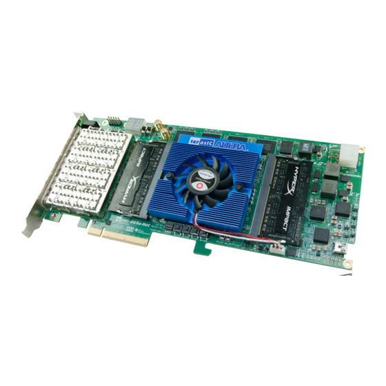
2.1 Board Overview Figure 2-1 is the top and bottom view of the DE5a-Net development board. It depicts the layout of the board and indicates the location of the connectors and key components. Users can refer to this figure for relative location of the connectors and key components. -
Page 13: Configuration, Status And Setup
USB-Blaster II driver is installed on PC. Launch Quartus II programmer and make sure the USB-Blaster II is detected. In Quartus II Programmer, add the configuration bit stream file (.sof), check DE5a-Net www.terasic.com User Manual March 22, 2018... - Page 14 Setup PCI Express Control DIP switch The PCI Express Control DIP switch (SW5) is provided to enable or disable different configurations of the PCIe Connector. Table 2-2lists the switch controls and description. DE5a-Net www.terasic.com User Manual March 22, 2018...
- Page 15 The position 1~3 of DIP switch SW3 are used to specify the configuration mode of the FPGA. As currently only one mode is supported, please set all positions as shown in Figure 2-3. Figure 2-3 Position of DIP switch SW3 for Configure Mode DE5a-Net www.terasic.com User Manual March 22, 2018...
- Page 16 2-4. Setting Position 4 of SW3 to “0” (up position) specifies the DE5a-Net to load a user-defined image, as shown inFigure 2-5. Figure 2-4 Position of DIP switch SW3 for Image Select – Factory Image Load Figure 2-5 Position of DIP switch SW3 for Image Select –...
-
Page 17: General User Input/Output
When a slide switch is in the DOWN position or the UPPER position, it provides a low logic level or a high logic level to the Arria 10 GX FPGA, respectively, as shown Figure 2-6. DE5a-Net www.terasic.com User Manual March 22, 2018... - Page 18 User-Defined LEDs The FPGA board consists of 8 user-controllable LEDs to allow status and debugging signals to be driven to the LEDs from the designs loaded into the Arria 10 GX device. DE5a-Net www.terasic.com User Manual March 22, 2018...
- Page 19 Each segment in a display is identified by an index listed from 0 to 6 with the positions given in Figure 2-8. In addition, the decimal point is identified as DP. Table 2-6 shows the mapping of the FPGA pin assignments to the 7-segment displays. DE5a-Net www.terasic.com User Manual March 22, 2018...
- Page 20 HEX1 HEX1_D2 1.5-V PIN_AM32 the 7-segment signal ON. Driving logic 1 on the I/O port turns the 7- HEX1 HEX1_D3 1.5-V PIN_AN32 segment signal OFF. HEX1 HEX1_D4 1.5-V PIN_AN31 HEX1 HEX1_D5 1.5-V PIN_AP31 DE5a-Net www.terasic.com User Manual March 22, 2018...
-
Page 21: Temperature Sensor And Fan Control
GX FPGA. In addition, the 7-bit POR slave address for this sensor is set to ‘0011000b’.Figure 2-9 shows theconnectionbetweenthetemperature sensor and the Arria 10 GX FPGA. Figure 2-9 Connections between the temperature sensor and the Arria 10 GX FPGA DE5a-Net www.terasic.com User Manual March 22, 2018... - Page 22 Arria 10 GX Pin Description I/O Standard Signal Name Number Positive pin of temperature TEMPDIODEp PIN_N21 diode in Arria 10 Negative pin of temperature TEMPDIODEn PIN_P21 diode in Arria 10 TEMP_I2C_SCL SMBus clock 1.5-V PIN_AU12 DE5a-Net www.terasic.com User Manual March 22, 2018...
-
Page 23: Power Monitor
1.5-V PIN_AL32 ERT input 2.5 Power Monitor The DE5a-Net has implemented a power monitor chip to monitor the board input power voltage and current. Figure 2-11 shows the connection between the power monitor chip and the Arria 10 GX FPGA. The power monitor chip monitors both shunt voltage drops and board input power voltage allows user to monitor the total board power consumption. -
Page 24: Clock Circuit
Arria 10 GX FPGA. Figure 2-12 Clock circuit of the FPGA Board A clock buffer is used to duplicate the 50 MHz oscillator, so there are five 50MHz clocks DE5a-Net www.terasic.com User Manual March 22, 2018... - Page 25 Defined 644.53125 40G QSFP+ A QSFPA_REFCLK_p LVDS PIN_AH5 port 644.53125 40G QSFP+ B QSFPB_REFCLK_p LVDS PIN_AD5 port 644.53125 40G QSFP+ C QSFPC_REFCLK_p LVDS PIN_Y5 port 644.53125 40G QSFP+ D QSFPD_REFCLK_p LVDS PIN_T5 port DE5a-Net www.terasic.com User Manual March 22, 2018...
- Page 26 Si5340A Si5340A_I2C_SDA 1.8-V PIN_AN8 Si5340A reset Si5340A_RST 1.8-V PIN_AN6 signal Si5340A Si5340A interrupt Si5340A_INTR 1.8-V PIN_AM6 (U15) signal Si5340A output Si5340A_OE_n 1.8-V PIN_AJ10 enable signal Si5340B Si5340B_I2C_SCL 1.8-V PIN_G37 I2C bus, connected DE5a-Net www.terasic.com User Manual March 22, 2018...
-
Page 27: Flash Memory
MAX V CPLD (5M2210) System Controller. Figure 2-13 shows the connections between the Flash, MAX and Arria 10 GX FPGA. Figure 2-13 Connection between the Flash, Max and Arria 10 GX FPGA DE5a-Net www.terasic.com User Manual March 22, 2018... - Page 28 Address bus 1.8-V PIN_A15 FLASH_A21 Address bus 1.8-V PIN_A14 FLASH_A22 Address bus 1.8-V PIN_H6 FLASH_A23 Address bus 1.8-V PIN_T12 FLASH_A24 Address bus 1.8-V PIN_U12 FLASH_A25 Address bus 1.8-V PIN_F7 FLASH_A26 Address bus 1.8-V PIN_B14 DE5a-Net www.terasic.com User Manual March 22, 2018...
- Page 29 Data bus 1.8-V PIN_K34 FLASH_D27 Data bus 1.8-V PIN_H38 FLASH_D28 Data bus 1.8-V PIN_H37 FLASH_D29 Data bus 1.8-V PIN_Y31 FLASH_D30 Data bus 1.8-V PIN_H35 FLASH_D31 Data bus 1.8-V PIN_J33 FLASH_CLK Clock 1.8-V PIN_T9 DE5a-Net www.terasic.com User Manual March 22, 2018...
-
Page 30: Ddr3 So-Dimm
933MHz memory clock for a maximum theoretical bandwidth up to 95.4Gbps. Figure 2-14 shows the connections between the DDR3 SDRAM SO- DIMMs and Arria 10 GX FPGA. DE5a-Net www.terasic.com User Manual March 22, 2018... - Page 31 Figure 2-14 Connection between the DDR3 and Arria 10 GX FPGA The pin assignments for DDR3 SDRAM SO-DIMM Bank-A and Bank-B are listed inTable 2-12andTable 2-13, in respectively. Table 2-12 DDR3-A Bank Pin Assignments, Schematic Signal Names, and Functions DE5a-Net www.terasic.com User Manual March 22, 2018...
- Page 32 Data [24] SSTL-15 PIN_AR36 DDR3A_DQ25 Data [25] SSTL-15 PIN_AN36 DDR3A_DQ26 Data [26] SSTL-15 PIN_AN38 DDR3A_DQ27 Data [27] SSTL-15 PIN_AN37 DDR3A_DQ28 Data [28] SSTL-15 PIN_AM38 DDR3A_DQ29 Data [29] SSTL-15 PIN_AM39 DDR3A_DQ30 Data [30] SSTL-15 PIN_AR37 DE5a-Net www.terasic.com User Manual March 22, 2018...
- Page 33 Data [57] SSTL-15 PIN_AU27 DDR3A_DQ58 Data [58] SSTL-15 PIN_AT30 DDR3A_DQ59 Data [59] SSTL-15 PIN_AR28 DDR3A_DQ60 Data [60] SSTL-15 PIN_AU29 DDR3A_DQ61 Data [61] SSTL-15 PIN_AV28 DDR3A_DQ62 Data [62] SSTL-15 PIN_AT29 DDR3A_DQ63 Data [63] SSTL-15 PIN_AR27 DE5a-Net www.terasic.com User Manual March 22, 2018...
- Page 34 Data Strobe n[6] PIN_BA27 SSTL Differential 1.5-V DDR3A_DQS7 Data Strobe p[7] PIN_AV30 SSTL Differential 1.5-V DDR3A_DQS_n7 Data Strobe n[7] PIN_AW30 SSTL DDR3A_DM0 Data Mask [0] SSTL-15 PIN_AK34 DDR3A_DM1 Data Mask [1] SSTL-15 PIN_AP35 DE5a-Net www.terasic.com User Manual March 22, 2018...
- Page 35 PIN_AP33 DDR3A_BA2 Bank Address [2] SSTL-15 Class I PIN_AR33 Differential 1.5-V DDR3A_CK0 Clock p0 PIN_BA34 SSTL Class I Differential 1.5-V DDR3A_CK_n0 Clock n0 PIN_BB35 SSTL Class I DDR3A_CK1 Clock p1 Differential 1.5-V PIN_BA35 DE5a-Net www.terasic.com User Manual March 22, 2018...
- Page 36 Data [2] SSTL-15 PIN_AP19 DDR3B_DQ3 Data [3] SSTL-15 PIN_AM19 DDR3B_DQ4 Data [4] SSTL-15 PIN_AM20 DDR3B_DQ5 Data [5] SSTL-15 PIN_AR18 DDR3B_DQ6 Data [6] SSTL-15 PIN_AM18 DDR3B_DQ7 Data [7] SSTL-15 PIN_AM17 DDR3B_DQ8 Data [8] SSTL-15 PIN_AY17 DE5a-Net www.terasic.com User Manual March 22, 2018...
- Page 37 Data [35] SSTL-15 PIN_AT6 DDR3B_DQ36 Data [36] SSTL-15 PIN_AU7 DDR3B_DQ37 Data [37] SSTL-15 PIN_AT7 DDR3B_DQ38 Data [38] SSTL-15 PIN_AT9 DDR3B_DQ39 Data [39] SSTL-15 PIN_AP10 DDR3B_DQ40 Data [40] SSTL-15 PIN_AK12 DDR3B_DQ41 Data [41] SSTL-15 PIN_AK13 DE5a-Net www.terasic.com User Manual March 22, 2018...
- Page 38 PIN_AT10 DDR3B_DQS_n3 Data Strobe n[3] Differential 1.5-V SSTL PIN_AU10 DDR3B_DQS4 Data Strobe p[4] Differential 1.5-V SSTL PIN_AV7 DDR3B_DQS_n4 Data Strobe n[4] Differential 1.5-V SSTL PIN_AV6 DDR3B_DQS5 Data Strobe p[5] Differential 1.5-V SSTL PIN_AG12 DE5a-Net www.terasic.com User Manual March 22, 2018...
- Page 39 SSTL-15 Class I PIN_AN13 DDR3B_A15 Address [15] SSTL-15 Class I PIN_AL14 Row Address DDR3B_RAS_n SSTL-15 Class I PIN_AM14 Strobe Column Address DDR3B_CAS_n SSTL-15 Class I PIN_AT14 Strobe DDR3B_BA0 Bank Address [0] SSTL-15 Class I PIN_AU14 DE5a-Net www.terasic.com User Manual March 22, 2018...
-
Page 40: Qdrii+ Sram
Each of QDRII+ has a x18 interface, providing addressing to a device of up to a 8MB (not including parity bits). The QDRII+ has separate read and write data ports with DDR signaling at up to 550 MHz. DE5a-Net www.terasic.com User Manual... - Page 41 Address bus[20] 1.8-V HSTL Class I PIN_K6 QDRIIA_A21 Address bus[21] 1.8-V HSTL Class I PIN_J6 QDRIIA_D0 Write data bus[0] 1.8-V HSTL Class I PIN_E8 QDRIIA_D1 Write data bus[1] 1.8-V HSTL Class I PIN_E9 DE5a-Net www.terasic.com User Manual March 22, 2018...
- Page 42 Read Data bus[13] 1.8-V HSTL Class I PIN_K13 QDRIIA_Q14 Read Data bus[14] 1.8-V HSTL Class I PIN_L14 QDRIIA_Q15 Read Data bus[15] 1.8-V HSTL Class I PIN_N13 QDRIIA_Q16 Read Data bus[16] 1.8-V HSTL Class I PIN_P13 DE5a-Net www.terasic.com User Manual March 22, 2018...
- Page 43 PIN_C15 QDRIIB_A8 Address bus[8] 1.8-V HSTL Class I PIN_F15 QDRIIB_A9 Address bus[9] 1.8-V HSTL Class I PIN_F16 QDRIIB_A10 Address bus[10] 1.8-V HSTL Class I PIN_H15 QDRIIB_A11 Address bus[11] 1.8-V HSTL Class I PIN_G15 DE5a-Net www.terasic.com User Manual March 22, 2018...
- Page 44 Read Data bus[1] 1.8-V HSTL Class I PIN_K23 QDRIIB_Q2 Read Data bus[2] 1.8-V HSTL Class I PIN_J23 QDRIIB_Q3 Read Data bus[3] 1.8-V HSTL Class I PIN_H23 QDRIIB_Q4 Read Data bus[4] 1.8-V HSTL Class I PIN_H21 DE5a-Net www.terasic.com User Manual March 22, 2018...
- Page 45 1.8-V HSTL Class I PIN_M17 Input Valid Output QDRIIB_QVLD 1.8-V HSTL Class I PIN_K22 Indicator Table 2-2 QDRII+ SRAM C Pin Assignments, Schematic Signal Names, and Functions Schematic Description I/O Standard Arria 10 GX Pin DE5a-Net www.terasic.com User Manual March 22, 2018...
- Page 46 Write data bus[6] 1.8-V HSTL Class I PIN_W34 QDRIIC_D7 Write data bus[7] 1.8-V HSTL Class I PIN_AC35 QDRIIC_D8 Write data bus[8] 1.8-V HSTL Class I PIN_AA35 QDRIIC_D9 Write data bus[9] 1.8-V HSTL Class I PIN_AF36 DE5a-Net www.terasic.com User Manual March 22, 2018...
- Page 47 QDRIIC_K_p PIN_AF34 Clock P Class I Differential 1.8-V HSTL QDRIIC_K_n PIN_AF35 Class I Clock N QDRIIC_CQ_p 1.8-V HSTL Class I PIN_AD36 Echo clock P QDRIIC_CQ_n 1.8-V HSTL Class I PIN_AC36 Echo clock N DE5a-Net www.terasic.com User Manual March 22, 2018...
- Page 48 PIN_L37 QDRIID_A16 Address bus[16] 1.8-V HSTL Class I PIN_K36 QDRIID_A17 Address bus[17] 1.8-V HSTL Class I PIN_N33 QDRIID_A18 Address bus[18] 1.8-V HSTL Class I PIN_M33 QDRIID_A19 Address bus[19] 1.8-V HSTL Class I PIN_L39 DE5a-Net www.terasic.com User Manual March 22, 2018...
- Page 49 Read Data bus[9] 1.8-V HSTL Class I PIN_G34 QDRIID_Q10 Read Data bus[10] 1.8-V HSTL Class I PIN_G33 QDRIID_Q11 Read Data bus[11] 1.8-V HSTL Class I PIN_L31 QDRIID_Q12 Read Data bus[12] 1.8-V HSTL Class I PIN_J31 DE5a-Net www.terasic.com User Manual March 22, 2018...
-
Page 50: Qspf+ Ports
Arria 10 GX FPGA device and transform them to optical signals. The board includes cage assemblies for the QSFP+ connectors. Figure 2-15 shows the connections between the QSFP+ and Arria 10 GX FPGA. DE5a-Net www.terasic.com User Manual March 22, 2018... - Page 51 PIN_AY6 Receiver data of channel 1 QSFPA_TX_P2 Transmitter data of channel 2 1.4-V PCML PIN_BB1 QSFPA_TX_N2 Transmitter data of channel 2 1.4-V PCML PIN_BB2 QSFPA_RX_P2 1.4-V PCML PIN_BA3 Receiver data of channel 2 DE5a-Net www.terasic.com User Manual March 22, 2018...
- Page 52 PIN_AH1 Transmitter data of channel 3 QSFPB_TX_N3 1.4-V PCML PIN_AH2 Transmitter data of channel 3 QSFPB_RX_P3 1.4-V PCML PIN_AG3 Receiver data of channel 3 QSFPB_RX_N3 1.4-V PCML PIN_AG4 Receiver data of channel 3 DE5a-Net www.terasic.com User Manual March 22, 2018...
- Page 53 Transmitter data of channel 3 QSFPC_TX_N3 1.4-V PCML PIN_T2 Transmitter data of channel 3 QSFPC_RX_P3 1.4-V PCML PIN_R3 Receiver data of channel 3 QSFPC_RX_N3 1.4-V PCML PIN_R4 Receiver data of channel 3 QSFPC_MOD_SEL_n Module Select 1.8V PIN_AL9 DE5a-Net www.terasic.com User Manual March 22, 2018...
- Page 54 Receiver data of channel 3 QSFPD_MOD_SEL_n Module Select 1.8V PIN_AA11 QSFPD_RST_n 1.8V PIN_Y11 Module Reset QSFPD_SCL 1.8V PIN_W9 2-wire serial interface clock QSFPD_SDA 1.8V PIN_W10 2-wire serial interface data QSFPD_LP_MODE Low Power Mode 1.8V PIN_AA12 DE5a-Net www.terasic.com User Manual March 22, 2018...
-
Page 55: Pci Express
PCI Express to allow different configurations to enable a x1, x4, or x8 PCIe. Table 2-22 summarizes the PCI Express pin assignments of the signal names relative to the Arria 10 GX FPGA. DE5a-Net www.terasic.com User Manual March 22, 2018... - Page 56 PIN_AK43 PCIE_TX_p5 Add-in card transmit bus 1.4-V PCML PIN_AH44 PCIE_TX_n5 Add-in card transmit bus 1.4-V PCML PIN_AH43 PCIE_TX_p6 Add-in card transmit bus 1.4-V PCML PIN_AF44 PCIE_TX_n6 Add-in card transmit bus 1.4-V PCML PIN_AF43 DE5a-Net www.terasic.com User Manual March 22, 2018...
- Page 57 Hot plug detect x1 PCIe slot PCIE_PRSNT2n_x1 enabled using SW5 dip switch Hot plug detect x4 PCIe slot PCIE_PRSNT2n_x4 enabled using SW5 dip switch Hot plug detect x8 PCIe slot PCIE_PRSNT2n_x8 enabled using SW5 dip switch DE5a-Net www.terasic.com User Manual March 22, 2018...
-
Page 58: Expansion Header
2-12 RS-422 Expansion Header The 2x5 RS-422 expansion header is designed to perform communication between boards. Users can use Terasic defined RS422-RJ45 board to translate RS-422 signal, allowing a transmission speed of up to 26 Mbps. Figure 2-17 shows the RS-422 application diagram. - Page 59 A high input forces the receiver output into a high impedancestate. DE5a-Net www.terasic.com User Manual March 22, 2018...
-
Page 60: Chapter 3 System Builder
The common mistakes that users encounter are the following: Board damaged for wrong pin/bank voltage assignment. Board malfunction caused by wrong device connections or missing pin counts DE5a-Net www.terasic.com User Manual March 22, 2018... -
Page 61: General Design Flow
The Quartus II setting file contains information such as FPGA device type, top-level pin assignment, and I/O standard for each user-defined I/O pin. Finally, Quartus II programmer must be used to download SOF file to the FPGA board using JTAG interface. DE5a-Net www.terasic.com User Manual March 22, 2018... -
Page 62: Using System Builder
The System Builder is located under the directory: "Tools\SystemBuilder" in the System CD. Users can copy the entire folder to the host computer without installing the utility. Please execute the SystemBuilder.exe on the host computer, as shown in Figure 3-2. DE5a-Net www.terasic.com User Manual March 22, 2018... - Page 63 Figure 3-2The System Builder window Enter Project Name The project name entered in the circled area as shown in Figure 3-3, will be assigned automatically as the name of the top-level design entry. DE5a-Net www.terasic.com User Manual March 22, 2018...
- Page 64 Quartus project or it would result in compilation error. Hence please do not select them if they are not needed in the design. To use the DDR3 controller, please refer to the DDR3 SDRAM demonstration in Chapter 6. DE5a-Net www.terasic.com User Manual...
- Page 65 Note: If users need to dynamically change the frequency, they would need to modify the generated control code themselves. DE5a-Net www.terasic.com User Manual March 22, 2018...
- Page 66 The System Builder also provides functions to restore default setting, load a setting, and save board configuration file, as shown in Figure 3-6. Users can save the current board configuration information into a .cfg file and load it into the System Builder. DE5a-Net www.terasic.com User Manual March 22, 2018...
- Page 67 Table 3-1 Files generated by the System Builder Filename Description <Project name>.v Top Level Verilog File for Quartus II Si5340_controller (*) Si5340A and Si5340BExternal Oscillator Controller IP <Project name>.qpf Quartus II Project File <Project name>.qsf Quartus II Setting File DE5a-Net www.terasic.com User Manual March 22, 2018...
- Page 68 SRAM Object File (.sof). For Si5340A, its controller will be instantiated in the Quartus II top-level file, as listed below: For Si5340B, its controller will be instantiated in the Quartus II top-level file, as listed below: DE5a-Net www.terasic.com User Manual March 22, 2018...
- Page 69 If the dynamic configuration for the oscillatoris required, users need to modify the code according to users’ desired behavior. DE5a-Net www.terasic.com User Manual March 22, 2018...
-
Page 70: Chapter 4 Flash Programming
User software and data 165,632 0x05E40000 – 0x0FFFFFFF For user application, user hardware must be stored with start address 0x02B40000, and the user’s software is suggested to be stored with start address 0x05E40000. The NIOS DE5a-Net www.terasic.com User Manual March 22, 2018... -
Page 71: Fpga Configure Operation
Power on the FPGA board or press MAX_RST button if board is already powered When configuration is completed, the green Configure Done LED will light. If there is error, the red Configure Error LED will light. Figure 4-1SW3 MSEL[0:2]=000 DE5a-Net www.terasic.com User Manual March 22, 2018... -
Page 72: Flash Programming With Users Design
Hardware design file for Hello Demo HELLO_NIOS.elf Software design file for Hello Demo To apply the batch file to users’.sof and .elf file, users can change the.sof and .elf filename in the flash_program.sh file as shown inFigure 4-3. DE5a-Net www.terasic.com User Manual March 22, 2018... - Page 73 Please ensure that the base address of the controller is 0x00, as shown in Figure 4-5. 2. In NIOS II processor options, select FLASH as reset vector memory and specify 0x05E40000 as reset vector, as shown in Figure 4-6. DE5a-Net www.terasic.com User Manual March 22, 2018...
-
Page 74: Restore Factory Settings
Make sure the Nios II EDS and USB-Blaster II driver are installed. Make sure the FPGA board and PC are connected with an UBS Cable. Power on the FPGA board. Copy the “Demonstrations/PFL/flash_programming_batch” folder under the CD to your PC’s local drive. DE5a-Net www.terasic.com User Manual March 22, 2018... - Page 75 Parallel Flasher Loader design in the FPGA. The Parallel Flash Loader design is included in the default code PFL and the source code is available in the folder Demonstrations/ PFL in System CD. DE5a-Net www.terasic.com User Manual March 22, 2018...
-
Page 76: Chapter 5 Peripheral Reference Design
The source codes and tool of these examples are all available on the System CD. 5.1 Temperature Monitor: Board Protection This section introduces a Terasic Temperature Monitor IP which can be used to monitor board temperature and raise an alert when the FPGA temperature reaches the specified threshold. Figure 5- 1 shows the block diagram for this demonstration. - Page 77 Provide 50 MHz clock signal to the IP TEMP_I2C_SCL output I2C SCL pin for Temperature Sensor TEMP_I2C_SDA In/out I2C SDA pin for Temperature Sensor Set alter temperature in degree C. Alert_Temperature[9:0] input Typically 80 is recommended. Do NOT exceed 95. DE5a-Net www.terasic.com User Manual March 22, 2018...
- Page 78 If the FPGA temperature exceed 80s degree, the LEDs will stop blinking. For test, please modify the Alert_Temperature to a lower value to so the measured temperature value can exceed the temperature specified by Alert_Temperature the in finally. DE5a-Net www.terasic.com User Manual March 22, 2018...
-
Page 79: Configure Si5340A/B In Rtl
5.2 Configure Si5340A/B in RTL There are two Silicon Labs Si5340 clock generators on DE5a-net FPGA board can provide adjustable frequency reference clock (See Figure 5- 2) for QSFP, QDRII , DDR3 and PCIe interfaces, etc. Each Si5340 clock generator can output four groups differential frequencies from 100Hz ~ 712.5Mhz though I2C interface configuration. - Page 80 4, if all the receiving Si5340 reference clock interface boxes are checked, then, every frequency channel of the two Si5340 chips is controllable by users. Figure 5- 3 Enable Si5340A clock on System Builder DE5a-Net www.terasic.com User Manual March 22, 2018...
- Page 81 Figure 5- 4 Enable Si5340A and Si5340BB clock on System Builder Click "Generate" button, then, open the Quartus Project generated by System Builder, the control IPs for Si5340A and Si5340B can be found in the top level file. DE5a-Net www.terasic.com User Manual...
- Page 82 SI5340B_RST_n = CPU_RESET_n; If the output frequency doesn’t need to be modified, users can just add their own User Logic and compile it, and then, Si5340 can output desired frequencies. At the same time, DE5a-Net www.terasic.com User Manual March 22, 2018...
- Page 83 Table 5- 2 Si5340 Controller Instruction Ports Port Direction Description iCLK input System Clock (50Mhz) Synchronous Reset (0: Module iRST_n input Reset, 1: Normal) Start to Configure(positive edge iStart input trigger) iPLL_OUTX_FREQ_SEL input Setting Si5340 Output Channel DE5a-Net www.terasic.com User Manual March 22, 2018...
- Page 84 125Mhz to 156.25Mhz. Table 5- 3 Si5340A Controller Frequency Setting iPLL_OUTX_FREQ_SEL Si5340A Channel Clock Frequency(MHz) MODE Setting 3'b000 Power Down 3'b001 644.53125 3'b010 322.26 3'b011 312.25 3'b100 3'b101 156.25 3'b110 3'b111 DE5a-Net www.terasic.com User Manual March 22, 2018...
- Page 85 Figure 5- 6), which is provided by Silicon Labs. This tool can help users to set the Si5340’s output frequency of each channel through the GUI interface, and it will automatically calculate the DE5a-Net www.terasic.com User Manual March 22, 2018...
- Page 86 Register parameters required for each frequency. The tool download link: http://www.silabs.com/products/clocksoscillators/pages/timing-software- development-tools.aspx Figure 5- 6 ClockBuilder Pro Wizard DE5a-Net www.terasic.com User Manual March 22, 2018...
- Page 87 Figure 5- 7 Define Output Clock Frequencies on ClockBuilder Pro Wizard After the setting is completed, ClockBuider Pro Wizard generates a Design Report(text), which contains users setting frequency corresponding register value (See Figure 5- DE5a-Net www.terasic.com User Manual March 22, 2018...
- Page 88 Open Si5340 control IP sub-module “si5340a_i2c_reg_controller.v “ as shown in Figure 5- 9, refer Design Report parameter to modify sub-module corresponding register value (See Figure 5- 10). Figure 5- 9 Sub-Module file "si5340a_i2c_reg_controller.v" DE5a-Net www.terasic.com User Manual March 22, 2018...
- Page 89 1. No need to modify all Design Report parameters in si5340a_i2c_reg_controller.v/si5340b_i2c_reg_controller.v, users can ignore parameters which have nothing to do with the frequency setting 2. After the manually modifying, please remember to modify clock constrain setting in .SDC file DE5a-Net www.terasic.com User Manual March 22, 2018...
-
Page 90: Nios Ii Control For Si5340/Temperature/Power
C code. The I2C pins from chip are connected to Qsys System Interconnect Fabric through PIO controllers. The Nios II program toggles the PIO controller to implement the I2C protocol. The Nios II program is running in the on-chip memory. DE5a-Net www.terasic.com User Manual March 22, 2018... - Page 91 With the menu, users can perform the test for the temperatures sensor, external PLL and power monitor. Note, pressing ‘ENTER’ should be followed with the choice number. Figure 5- 12 Menu of Demo Program DE5a-Net www.terasic.com User Manual March 22, 2018...
- Page 92 There is a shunt resistor R149 (RSHUNT =0.003 Ω) for INA231AIYFFT in the circuit, when power on the DE5a-NET board, there will be a voltage drop (named Shut Voltage) on R149. Based on sense resistors, the program of power monitor can calculate the associated voltage, current and power consumption from the IN231 through the I2C interface.
- Page 93 For programmable PLL Si5340B test, please input key ‘3’ and press ‘Enter’ in the nios-terminal first, then select the desired output frequency of DDR3/PCIE/QDRII REFCLK, as shown in Figure 5- Figure 5- 13 Temperature Demo DE5a-Net www.terasic.com User Manual March 22, 2018...
- Page 94 Figure 5- 14 power monitor Demo DE5a-Net www.terasic.com User Manual March 22, 2018...
- Page 95 Figure 5- 15 Si5340A Demo DE5a-Net www.terasic.com User Manual March 22, 2018...
-
Page 96: Fan Speed Control
The following section will save lots of time for the development of user application. System Block Diagram Figure 5- 17 shows the system block diagram of this demo. It is necessary to configure DE5a-Net www.terasic.com User Manual March 22, 2018... - Page 97 The status of BIT 4 ~ 7 can be ignored because BIT 4 is for MAX6651 only and BIT 5 ~ 7 are always low. DE5a-Net www.terasic.com User Manual...
- Page 98 Project Directory: Demonstration\Fan Bit Stream: DE5a_NET_golden_top.sof Demonstration Batch File Demo Batch File Folder: \Fan\demo_batch The demo batch file includes following files: Batch File: test_ub2.bat FPGA Configure File: DE5a_NET_folden_top.sof Demonstration Setup DE5a-Net www.terasic.com User Manual March 22, 2018...
- Page 99 Make sure Quartus II is installed on the host PC. Connect the DE5a-Net and the host PC via USB cable. Install the USB-Blaster II driver if necessary. Power on the FPGA Board. Execute the demo batch file “test_ub2.bat” under the batch file folder \Fan\demo_batch.
-
Page 100: Chapter 6 Memory Reference Design
DD3 SDRAM Test: Random test of the two banks of DDR3 SDRAM. DDR3 SDRAM Test by Nios II: Full test of one bank of DDR3 SDRAM with Nios II Note. 64-Bit Quartus15.0 or later is strongly recommended for compiling these projects. DE5a-Net www.terasic.com User Manual March 22, 2018... -
Page 101: Qdrii+ Sram Test
This demonstration utilizes four QDRII+ SRAMs on the FPGA board. It describes how to use Altera’s “Arria 10 External Memory Interfaces” (Arria 10 EMIF) IP to implement a memory test function. Function Block Diagram DE5a-Net www.terasic.com User Manual March 22, 2018... - Page 102 Figure 6-1Function Block Diagram of the QDRII+ SRAM x4 Demonstration The QDRIIA/B/C/D_REFCLK is generated from Si5340B which configured 275MHz for QDRII+ 550MHz by Clock Config module. QDRIIA/B/C/D_REFCLK has no default frequency output so that they must be configured first. DE5a-Net www.terasic.com User Manual March 22, 2018...
- Page 103 Quartus II 15.1 Demonstration Source Code Project directory: QDRIIx4_Test Bit stream used: QDRIIx4_Test.sof Demonstration Batch File Demo Batch File Folder: QDRIIx4_Test\demo_batch The demo batch files include the followings: DE5a-Net www.terasic.com User Manual March 22, 2018...
-
Page 104: Ddr3 Sdram Test
QDRII+ SRAM(D) test result 6.2 DDR3 SDRAM Test This demonstration performs a memory test function on the two DDR3-SDRAM SO- DIMM on the DE5a-Net. The memory size of each DDR3 SDRAM SO-DIMM used in this test is 4 GB. Function Block Diagram DE5a-Net www.terasic.com... - Page 105 Altera DDR3 SDRAM Controller with UniPHY To use Altera DDR3 controller, please perform the three major steps below: 1. Create correct pin assignments for DDR3. 2. Setup correct parameters in the dialog of DDR3 controller. DE5a-Net www.terasic.com User Manual March 22, 2018...
- Page 106 FPGA Configuration File: DE5A_NET_4GB.sof Demonstration Setup Make sure Quartus II is installed on the host PC. Connect DE5a-Net board to the host PC via USB cable. Install the USB-Blaster II driver if necessary. Power on the DE5a-Net board. ...
-
Page 107: Ddr3 Sdram Test By Nios Ii
System Block Diagram Figure 6-3 shows the system block diagram of this demonstration. The QSYS system requires one 50 MHz and two 200MHz clock source. The two 200 MHz clock source is DE5a-Net www.terasic.com User Manual March 22, 2018... - Page 108 SDRAM. Finally, it reads data from SDRAM for data verification. The program will show progress in JTAG- Terminal when writing/reading data to/from the SDRAM. When verification process is completed, the result is displayed in the JTAG-Terminal. DE5a-Net www.terasic.com User Manual March 22, 2018...
- Page 109 The demo batch file includes following files: Batch File for USB-Blaseter II: test.bat, test.sh FPGA Configure File: DE5A_NET.sof Nios II Program: TEST_MEM.elf Demonstration Setup Please follow below procedures to setup the demonstartons. DE5a-Net www.terasic.com User Manual March 22, 2018...
- Page 110 Press Button3~Button0 of the FPGA board to start SDRAM verify process. Press Button0 for continued test. The program will display progressing and result information, as shown in Figure 6-4. Figure 6-4 Display Progress and Result Information for the DDR3 Demonstration DE5a-Net www.terasic.com User Manual March 22, 2018...
-
Page 111: Chapter 7 Pci Express Reference Design For Windows
It consists of two primary components: FPGA System and PC System. The FPGA System is developed based on Arria 10 Hard IP for PCI Express with Avalon-MM DMA. The application software on the PC side is developed by Terasic based on Altera’s PCIe kernel mode driver. -
Page 112: Pc Pci Express Software Sdk
PCI Express Examples The kernel mode driver assumes the PCIe vendor ID (VID) is 0x1172 and the device ID (DID) is 0xE003. If different VID and DID are used in the design, users need to modify DE5a-Net www.terasic.com User Manual... -
Page 113: Pci Express Software Stack
Windows. The PCIe library module TERASIC_PCIE_AVMM.dll provides DMA and direct I/O access for user application program to communicate with FPGA. Users can develop their applications based on this DLL. The altera_pcie_win_driver.sys kernel driver is provided by Altera. DE5a-Net www.terasic.com User Manual March 22, 2018... - Page 114 The folder includes the following four files: Altera_pcie_win_driver.cat Altera_pcie_win_driver.inf Altera_pcie_win_driver.sys WdfCoinstaller01011.dll To install the PCI Express driver, please execute the steps below: 1. Install the DE5a-Net on the PCIe slot of the host PC DE5a-Net www.terasic.com User Manual March 22, 2018...
- Page 115 Figure 7-3 Screenshot of launching Update Driver Software… dialog 6. In the How do you want to search for driver software dialog, click Browse my computer for driver software item, as shown in Figure 7-4 DE5a-Net www.terasic.com User Manual March 22, 2018...
- Page 116 7. In the Browse for driver software on your computer dialog, click the Browse button to specify the folder where altera_pcie_din_driver.inf is located, as shown Figure 7-5. Click the Next button. Figure 7-5 Browse for driver software on your computer DE5a-Net www.terasic.com User Manual March 22, 2018...
- Page 117 9. When the driver is installed successfully, the successfully dialog will appears, as shown in Figure 7-7. Click the Close button. Figure 7-7 Click Close when the installation of Altera PCI API Driver is complete DE5a-Net www.terasic.com User Manual March 22, 2018...
- Page 118 CDROM\demonstration\PCIe_SW_KIT\Windows\PCIe_Library. It includes the following files: TERASIC_PCIE_AVMM.h TERASIC_PCIE_AVMM.DLL (64-bit DLL) Below lists the procedures to use the SDK files in users’ C/C++ project: Create a 64-bit C/C++ project. Include TERASIC_PCIE_AVMM.h in the C/C++ project. DE5a-Net www.terasic.com User Manual March 22, 2018...
-
Page 119: Pci Express Library Api
Specify the matched card index, a zero based index, based on the matched vendor ID and device ID. Return Value: Return a handle to presents specified PCIe card. A positive value is return if the PCIe DE5a-Net www.terasic.com User Manual March 22, 2018... - Page 120 Prototype: bool PCIE_Read32( PCIE_HANDLE hPCIE, PCIE_BAR PcieBar, PCIE_ADDRESS PcieAddress, uint32_t *pdwData); Parameters: hPCIE: A PCIe handle return by PCIE_Open function. PcieBar: Specify the target BAR. PcieAddress: Specify the target address in FPGA. pdwData: DE5a-Net www.terasic.com User Manual March 22, 2018...
- Page 121 Return Value: Return true if write data is successful; otherwise false is returned. PCIE_Read8 Function: Read an 8-bit data from the FPGA board. Prototype: bool PCIE_Read8( PCIE_HANDLE hPCIE, PCIE_BAR PcieBar, PCIE_ADDRESS PcieAddress, DE5a-Net www.terasic.com User Manual March 22, 2018...
- Page 122 Specify the target BAR. PcieAddress: Specify the target address in FPGA. Byte: Specify an 8-bit data which will be written to FPGA board. Return Value: Return true if write data is successful; otherwise false is returned. DE5a-Net www.terasic.com User Manual March 22, 2018...
- Page 123 Return true if read data is successful; otherwise false is returned. PCIE_DmaWrite Function: Write data to the memory-mapped memory of FPGA board in DMA. Prototype: bool PCIE_DmaWrite( PCIE_HANDLE hPCIE, PCIE_LOCAL_ADDRESS LocalAddress, void *pData, DE5a-Net www.terasic.com User Manual March 22, 2018...
- Page 124 Offset: Specify the target byte of offset in PCIe configuration table. pdwData: A 4-bytes buffer to retrieve the 32-bit data. Return Value: Return true if read data is successful; otherwise false is returned. DE5a-Net www.terasic.com User Manual March 22, 2018...
-
Page 125: Pcie Reference Design - Fundamental
Download Batch file: test.bat Windows Application Software folder : windows_app, includes PCIE_FUNDAMENTAL.exe TERASIC_PCIE_AVMM.dll Demonstration Setup 1. Install the FPGA board on your PC as shown in Figure 7-9. DE5a-Net www.terasic.com User Manual March 22, 2018... - Page 126 3. Install PCIe driver if necessary. The driver is located in the folder: CDROM\Demonstration\PCIe_SW_KIT\Windows\PCIe_Driver. 4. Restart Windows 5. Make sure the Windows has detected the FPGA Board by checking the Windows Control panel as shown in Figure 7-10. DE5a-Net www.terasic.com User Manual March 22, 2018...
- Page 127 Figure 7-10 Screenshot for PCIe Driver 6. Goto windows_app folder, execute PCIE_FUNDMENTAL.exe. A menu will appear as shown in Figure 7-11. Figure 7-11 Screenshot of Program Menu DE5a-Net www.terasic.com User Manual March 22, 2018...
- Page 128 Figure 7-13. Figure 7-13 Screenshot of Button Status Report 9. Type 2 followed by an ENTERY key to select DMA Testing item. The DMA test result DE5a-Net www.terasic.com User Manual March 22, 2018...
- Page 129 FPGA Application Design Figure 7-15 shows the system block diagram in the FPGA system. In the Qsys, Altera PIO controller is used to control the LED and monitor the Button Status, and the On- DE5a-Net www.terasic.com User Manual March 22, 2018...
- Page 130 Implement dynamically load for TERAISC_PCIE_AVMM.DLL PCIE.h TERASIC_PCIE_AVMM.h SDK library file, defines constant and data structure The main program PCIE_FUNDAMENTAL.cpp includes the header file "PCIE.h" and defines the controller address according to the FPGA design. DE5a-Net www.terasic.com User Manual March 22, 2018...
- Page 131 The LED control is implemented by calling PCIE_Write32 API, as shown below: The button status query is implemented by calling the PCIE_Read32 API, as shown below: The memory-mapped memory read and write test is implemented by PCIE_DmaWrite DE5a-Net www.terasic.com User Manual March 22, 2018...
-
Page 132: Pcie Reference Design - Ddr3
2. Install the FPGA board on your PC. 3. Configure FPGA with DE5A_NET.sof by executing the test.bat. 4. Install PCIe driver if necessary. 5. Restart Windows 6. Make sure the Windows has detected the FPGA Board by checking the Windows DE5a-Net www.terasic.com User Manual March 22, 2018... - Page 133 Control panel. 7. Goto windows_app folder, execute PCIE_DDR3.exe. A menu will appear as shown Figure 7-16. Figure 7-16 Screenshot of Program Menu DE5a-Net www.terasic.com User Manual March 22, 2018...
- Page 134 9. Type 3 followed by an ENTERY key to select DMA On-Chip Memory Test item. The DMA write and read test result will be report as shown in Figure 7-18. Figure 7-18 Screenshot of On-Chip Memory DMA Test Result DE5a-Net www.terasic.com User Manual March 22, 2018...
- Page 135 Figure 7-19 Screenshot of DDR3-A SOSIMM Memory DAM Test Result 11. Type 5 followed by an ENTERY key to select DMA DDR3-B SODIMM Memory Test item. The DMA write and read test result will be report as shown in Figure 7-20. DE5a-Net www.terasic.com User Manual March 22, 2018...
- Page 136 Figure 7-20 Screenshot of DDR3-B SOSIMM Memory DAM Test Result 12. Type 99 followed by an ENTERY key to exit this test program. DE5a-Net www.terasic.com User Manual March 22, 2018...
- Page 137 Chip memory is used for performing DMA testing. The PIO controllers and the On-Chip memory are connected to the PCI Express Hard IP controller through the Memory- Mapped Interface. Figure 7-21 Hardware block diagram of the PCIe_DDR3 reference design DE5a-Net www.terasic.com User Manual March 22, 2018...
- Page 138 PCIE_Open are defined in TERASIC_PCIE_AVMM.h. If developer change the Vendor ID and Device ID and PCI Express IP, they also need to change the ID value define in TERASIC_PCIE_AVMM.h. If the return value of PCIE_Open is zero, it means DE5a-Net www.terasic.com User Manual...
- Page 139 The button status query is implemented by calling the PCIE_Read32 API, as shown below: The memory-mapped memory read and write test is implemented by PCIE_DmaWrite and PCIE_DmaRead API, as shown below: The PCIe link information is implemented by PCIE_ConfigRead32 API, as shown below: DE5a-Net www.terasic.com User Manual March 22, 2018...
- Page 140 DE5a-Net www.terasic.com User Manual March 22, 2018...
-
Page 141: Chapter 8 Pci Express Reference Design For Linux
It consists of two primary components: FPGA System and PC System. The FPGA System is developed based on Arria 10 Hard IP for PCI Express with Avalon-MM DMA. The application software on the PC side is developed by Terasic based on Altera’s PCIe kernel mode driver. -
Page 142: Pc Pci Express Software Sdk
The kernel mode driver assumes the PCIe vendor ID (VID) is 0x1172 and the device ID (DID) is 0xE003. If different VID and DID are used in the design, users need to modify the PCIe vendor ID (VID) and device ID (DID) in the driver project and rebuild the driver. DE5a-Net www.terasic.com User Manual... -
Page 143: Pci Express Software Stack
Linux. The PCIe library module terasic_pcie_qys.so provides DMA and direct I/O access for user application program to communicate with FPGA. Users can develop their applications based on this .so library file. The altera_pcie.ko kernel driver is provided by Altera. DE5a-Net www.terasic.com User Manual March 22, 2018... - Page 144 The folder includes the following files: altera_pcie.c altera_pcie.h altera_pcie_cmd.h Makefile load_driver unload config_file To compile and install the PCI Express driver, please execute the steps below: DE5a-Net www.terasic.com User Manual March 22, 2018...
- Page 145 1. Install the DE5a-Net on the PCIe slot of the host PC 2. Make sure Altera Programmer and USB-Blaster II driver are installed 3. Open a terminal and use "cd" command to goto the folder "CDROM/Demonstrations/PCIe_Fundamental/demo_batch". 4. Set QUARTUS_ROOTDIR variable pointing to the Quartus installation path. Set QUARTUS_ROOTDIR variable by tying the following commands in terminal.
-
Page 146: Pci Express Library Api
DMA. In the design, basic I/O is used to control the BUTTON and LED on the FPGA board. High-speed data transfer is performed by DMA. Demonstration Files Location The demo file is located in the batch folder: DE5a-Net www.terasic.com User Manual March 22, 2018... - Page 147 2. Open a terminal and use "cd" command to goto "CDROM/Demonstrations/PCIe_Fundamental/demo_batch". 3. Set QUARTUS_ROOTDIR variable pointing to the Quartus installation path. Set QUARTUS_ROOTDIR variable by tying the following commands in terminal. Replace /home/centos/altera/15.1/quartus to your quartus installation path. DE5a-Net www.terasic.com User Manual March 22, 2018...
- Page 148 9. Type 0 followed by a ENTERY key to select Led Control item, then input 15 (hex 0x0f) will make all led on as shown in Figure 8-6. If input 0 (hex 0x00), all led will be turn off. DE5a-Net www.terasic.com User Manual March 22, 2018...
- Page 149 Figure 8-6 Screenshot of LED Control 10. Type 1 followed by an ENTERY key to select Button Status Read item. The button status will be report as shown in Figure 8-7. Figure 8-7 Screenshot of Button Status Report DE5a-Net www.terasic.com User Manual March 22, 2018...
- Page 150 PIO controller is used to control the LED and monitor the Button Status, and the On- Chip memory is used for performing DMA testing. The PIO controllers and the On-Chip memory are connected to the PCI Express Hard IP controller through the Memory- DE5a-Net www.terasic.com User Manual...
- Page 151 Implement dynamically load for terasic_pcie_qsys.so library file PCIE.h TERASIC_PCIE_AVMM.h SDK library file, defines constant and data structure The main program PCIE_FUNDAMENTAL.cpp includes the header file "PCIE.h" and defines the controller address according to the FPGA design. DE5a-Net www.terasic.com User Manual March 22, 2018...
- Page 152 The LED control is implemented by calling PCIE_Write32 API, as shown below: The button status query is implemented by calling the PCIE_Read32 API, as shown below: The memory-mapped memory read and write test is implemented by PCIE_DmaWrite DE5a-Net www.terasic.com User Manual March 22, 2018...
-
Page 153: Pcie Reference Design - Ddr3
1. Install both DDR3 2133 4GB SODIMM on the FPGA board. 2. Install the FPGA board on your PC. 3. Open a terminal and use "cd" command to goto "CDROM/Demonstrations/PCIe_DDR3/demo_batch". 4. Set QUARTUS_ROOTDIR variable pointing to the Quartus installation path. Set DE5a-Net www.terasic.com User Manual March 22, 2018... - Page 154 10. Type 2 followed by an ENTERY key to select Link Info item. The PCIe link information will be shown as in Figure 8-11. Gen3 link speed and x8 link width are expected. DE5a-Net www.terasic.com User Manual March 22, 2018...
- Page 155 11. Type 3 followed by an ENTERY key to select DMA On-Chip Memory Test item. The DMA write and read test result will be report as shown in Figure 8-12. Figure 8-12 Screenshot of On-Chip Memory DMA Test Result DE5a-Net www.terasic.com User Manual March 22, 2018...
- Page 156 The DMA write and read test result will be report as shown in Figure 8-15. Figure 8-15 Screenshot of DDR3-B SOSIMM Memory DAM Test Result 14. Type 99 followed by an ENTERY key to exit this test program. DE5a-Net www.terasic.com User Manual March 22, 2018...
- Page 157 Chip memory is used for performing DMA testing. The PIO controllers and the On-Chip memory are connected to the PCI Express Hard IP controller through the Memory- Mapped Interface. Figure 8-16 Hardware block diagram of the PCIe_DDR3 reference design DE5a-Net www.terasic.com User Manual March 22, 2018...
- Page 158 PCIE_Open are defined in TERASIC_PCIE_AVMM.h. If developer change the Vendor ID and Device ID and PCI Express IP, they also need to change the ID value define in TERASIC_PCIE_AVMM.h. If the return value of PCIE_Open is zero, it means the driver DE5a-Net www.terasic.com User Manual...
- Page 159 The button status query is implemented by calling the PCIE_Read32 API, as shown below: The memory-mapped memory read and write test is implemented by PCIE_DmaWrite and PCIE_DmaRead API, as shown below: The PCIe link information is implemented by PCIE_ConfigRead32 API, as shown below: DE5a-Net www.terasic.com User Manual March 22, 2018...
- Page 160 DE5a-Net www.terasic.com User Manual March 22, 2018...
-
Page 161: Chapter 9 Transceiver Verification
Transceiver Verification his chapter describes how to verify the FPGA transceivers for the QSFP+ by using the test code provided in the DE5a-Net system CD. 9.1 Function of the Transceiver Test Code The transceiver test code is used to verify the transceiver channels for the QSPF+ ports through an external loopback method. - Page 162 Figure 9-1 Optical QSFP+ Cable Figure 9-2 QSFP+ Loopback Fixture Figure 9-3 shows the FPGA board with two QSFP+ cable installed. Figure 9-4 shows the FPGA board with four QSFP+ loopback fixtures installed. DE5a-Net www.terasic.com User Manual March 22, 2018...
- Page 163 Figure 9-3 Two QSFP+ Cables Installed Figure 9-4 Four QSFP+ Loopback Fixtures Installed DE5a-Net www.terasic.com User Manual March 22, 2018...
-
Page 164: Testing
The test result is shown in the Nios-Terminal, as shown in Figure 9-5. To terminate the test, press one of the BUTTON0~3 buttons on the FPGA board. The loopback test will terminate as shown in Figure 9-6. DE5a-Net www.terasic.com User Manual March 22, 2018... - Page 165 Figure 9-5 QSFP+ Transceiver Loopback Test in Progress Figure 9-6 QSFP+ Transceiver Loopback Done DE5a-Net www.terasic.com User Manual March 22, 2018...
-
Page 166: Additional Information
Here are the addresses where you can get help if you encounter problems: Terasic Technologies 9F., No.176, Sec.2, Gongdao 5th Rd, East Dist, HsinChu City, Taiwan, 30070 Email: support@terasic.com Web: www.terasic.com DE5a-Net Web: DE5a-Net.terasic.com Revision History Date Version Changes 2016.01 First publication 2016.10.24...
Need help?
Do you have a question about the DE5a-Net and is the answer not in the manual?
Questions and answers