Terasic DE0-Nano-SoC User Manual
Hide thumbs
Also See for DE0-Nano-SoC:
- User manual (50 pages) ,
- Getting started manual (26 pages) ,
- Design manual (100 pages)
Table of Contents
Advertisement
Advertisement
Table of Contents

Related Manuals for Terasic DE0-Nano-SoC


Summary of Contents for Terasic DE0-Nano-SoC
- Page 1 DE0-Nano-SoC www.terasic.com User Manual August 31, 2017...
-
Page 2: Table Of Contents
Chapter 3 Using the DE0-Nano-SoC Board ..........12 3.1 Settings of FPGA Configuration Mode ..................12 3.2 Configuration of Cyclone V SoC FPGA on DE0-Nano-SoC ........... 14 3.3 Board Status Elements ......................19 3.4 Board Reset Elements ......................20 3.5 Clock Circuitry ......................... 21 3.6 Peripherals Connected to the FPGA .................. - Page 3 Chapter 4 DE0-Nano-SoC System Builder ........... 42 4.1 Introduction ..........................42 4.2 Design Flow ..........................42 4.3 Using DE0-Nano-SoC System Builder ..................43 Chapter 5 Examples For FPGA ..............49 5.1 DE0-Nano-SoC Factory Configuration ..................49 5.2 ADC Reading ........................... 50 Chapter 6 Examples for HPS SoC ..............
- Page 4 9.1 What's different between the DE0-Nano-SoC kit and the Atlas-SoC kit?........ 78 Chapter 10 Appendix B ..................79 10.1 Revision History ........................79 10.2 Copyright Statement ....................... 79 DE0-Nano-SoC www.terasic.com User Manual August 31, 2017...
-
Page 5: De0-Nano-Soc Development Kit
In addition, DE0-Nano-SoC Kit is also called Atlas-SoC Kit in Altera's Rockboard.org Linux community (http://www.rocketboards.org/atlas-soc). The hardware of DE0-Nano-SoC Kit and Atlas-SoC Kit are exactly the same, however, this community provides different development resource from DE0-Nano-SoC Kit. The details of kit contents can be found in the Appendix chapter. DE0-Nano-SoC www.terasic.com... -
Page 6: Package Contents
5V/2A DC power adapter 4GB microSD Card (Installed) The DE0-Nano-SoC System CD contains all the documents and supporting materials associated with DE0-Nano-SoC, including the user manual, system builder, reference designs, and device datasheets. Users can download this system CD from the link: http://cd-de0-nano-soc.terasic.com. -
Page 7: Getting Help
Here are the addresses where you can get help if you encounter any problems: Altera Corporation 101 Innovation Drive San Jose, California, 95134 USA Email: university@altera.com Terasic Technologies 9F., No.176, Sec.2, Gongdao 5th Rd, East Dist, Hsinchu City, 30070. Taiwan Email: support@terasic.com Tel.: +886-3-575-0880 Website: de0-nano-soc.terasic.com... -
Page 8: Introduction Of The De0-Nano-Soc Board
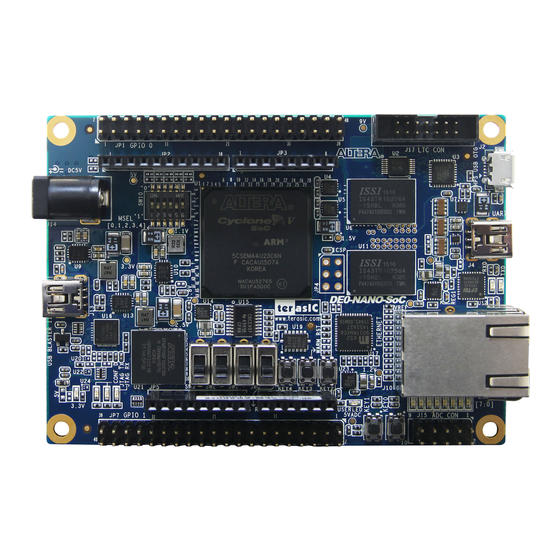
Figure 2-1 Figure 2-2 shows a photograph of the board. It depicts the layout of the board and indicates the location of the connectors and key components. Figure 2-1 DE0-Nano-SoC development board (top view) DE0-Nano-SoC www.terasic.com User Manual August 31, 2017... - Page 9 Figure 2-2 DE0-Nano-SoC development board (bottom view) The DE0-Nano-SoC board has many features that allow users to implement a wide range of designed circuits, from simple circuits to various multimedia projects. The following hardware is provided on the board: FPGA ...
-
Page 10: Block Diagram Of The De0-Nano-Soc Board
All the connections are established through the Cyclone V SoC FPGA device to provide maximum flexibility for users. Users can configure the FPGA to implement any system design. DE0-Nano-SoC www.terasic.com User Manual August 31, 2017... - Page 11 Figure 2-3 Block diagram of DE0-Nano-SoC Detailed information about Figure 2-3 are listed below. Cyclone V SoC 5CSEMA4U23C6N Device Dual-core ARM Cortex-A9 (HPS) 40K programmable logic elements 2,460 Kbits embedded memory 5 fractional PLLs 2 hard memory controllers ...
- Page 12 3 user Keys (FPGA x2, HPS x1) 4 user switches (FPGA x4) 9 user LEDs (FPGA x8, HPS x 1) 2 HPS reset buttons (HPS_RESET_n and HPS_WARM_RST_n) G-Sensor on HPS 5V DC input DE0-Nano-SoC www.terasic.com User Manual August 31, 2017...
-
Page 13: Chapter 3 Using The De0-Nano-Soc Board
This chapter provides an instruction to use the board and describes the peripherals. When the DE0-Nano-SoC board is powered on, the FPGA can be configured from EPCS or HPS. The MSEL[4:0] pins are used to select the configuration scheme. It is implemented as a 6-pin DIP... - Page 14 If developers using the "Linux Console with frame buffer" or "Linux LXDE Desktop" SD Card image, the MSEL[4:0] needs to be set to “00000” before the board is powered on. Table 3-2 MSEL Pin Settings for FPGA Configure of DE0-Nano-SoC SW10.1 SW10.2 SW10.3...
-
Page 15: Configuration Of Cyclone V Soc Fpga On De0-Nano-Soc
The information is retained within EPCS even if the DE0-Nano-SoC board is turned off. When the board is powered on, the configuration data in the EPCS device is automatically loaded into the Cyclone V SoC FPGA. - Page 16 Open the Quartus II programmer and click “Auto Detect”, as circled in Figure 3-3 Figure 3-3 Detect FPGA device in JTAG mode Select detected device associated with the board, as circled in Figure 3-4. Figure 3-4 Select 5CSEMA4 device DE0-Nano-SoC www.terasic.com User Manual August 31, 2017...
- Page 17 Figure 3-5 FPGA and HPS detected in Quartus programmer Right click on the FPGA device and open the .sof file to be programmed, as highlighted in Figure 3-6. Figure 3-6 Open the .sof file to be programmed into the FPGA device DE0-Nano-SoC www.terasic.com User Manual August 31, 2017...
- Page 18 Figure 3-7 Select the .sof file to be programmed into the FPGA device Click “Program/Configure” check box and then click “Start” button to download the .sof file into the FPGA device, as shown in Figure 3-8. Figure 3-8 Program .sof file into the FPGA device DE0-Nano-SoC www.terasic.com User Manual August 31, 2017...
- Page 19 Configure the FPGA in AS Mode The DE0-Nano-SoC board uses a serial configuration device (EPCS) to store configuration data for the Cyclone V SoC FPGA. This configuration data is automatically loaded from the serial configuration device chip into the FPGA when the board is powered up.
-
Page 20: Board Status Elements
In addition to the 9 LEDs that FPGA/HPS device can control, there are 6 indicators which can indicate the board status (See Figure 3-10), please refer the details in Table 3-3 Figure 3-10 LED Indicators on DE0-Nano-SoC Table 3-3 LED Indicators Board Reference LED Name Description LED9 3.3-V Power... -
Page 21: Board Reset Elements
There are two HPS reset buttons on DE0-Nano-SoC, HPS (cold) reset and HPS warm reset, as shown in Figure 3-11. Table 3-4 describes the purpose of these two HPS reset buttons. Figure 3-12 is the reset tree for DE0-Nano-SoC. Figure 3-11 HPS cold reset and warm reset buttons on DE0-Nano-SoC... -
Page 22: Clock Circuitry
Figure 3-12 HPS reset tree on DE0-Nano-SoC board Figure 3-13 shows the default frequency of all external clocks to the Cyclone V SoC FPGA. A clock generator is used to distribute clock signals with low jitter. The two 50MHz clock signals connected to the FPGA are used as clock sources for user logic. -
Page 23: Peripherals Connected To The Fpga
Figure 3-13 Block diagram of the clock distribution on DE0-Nano-SoC Table 3-5 Pin Assignment of Clock Inputs Signal Name FPGA Pin No. Description I/O Standard FPGA_CLK1_50 PIN_V11 50 MHz clock input 3.3V FPGA_CLK2_50 PIN_Y13 50 MHz clock input 3.3V FPGA_CLK3_50 PIN_E11 50 MHz clock input (share with FPGA_CLK1_50) 3.3V... -
Page 24: User Push-Buttons, Switches And Leds
Figure 3-14 Connections between the push-buttons and the Cyclone V SoC FPGA Pushbutton depressed Pushbutton released Before Debouncing Schmitt Trigger Debounced Figure 3-15 Switch debouncing There are four slide switches connected to the FPGA, as shown in Figure 3-16. These switches are DE0-Nano-SoC www.terasic.com User Manual August 31, 2017... - Page 25 LED on or off, respectively. Figure 3-17 shows the connections between LEDs and Cyclone V SoC FPGA. Table 3-6, Table 3-7 Table 3-8 list the pin assignment of user push-buttons, switches, and LEDs. DE0-Nano-SoC www.terasic.com User Manual August 31, 2017...
- Page 26 LED [1] 3.3V LED[2] PIN_V16 LED [2] 3.3V LED[3] PIN_V15 LED [3] 3.3V LED[4] PIN_AF26 LED [4] 3.3V LED[5] PIN_AE26 LED [5] 3.3V LED[6] PIN_Y16 LED [6] 3.3V LED[7] PIN_AA23 LED [7] 3.3V DE0-Nano-SoC www.terasic.com User Manual August 31, 2017...
-
Page 27: 2X20 Gpio Expansion Headers
PIN_AH19 GPIO_1[28] GPIO_1[29] PIN_AH21 PIN_AD11 GPIO_0[30] GPIO_0[31] PIN_AF10 PIN_AG21 GPIO_1[30] GPIO_1[31] PIN_AH18 PIN_AD12 GPIO_0[32] GPIO_0[33] PIN_AE11 PIN_AD23 GPIO_1[32] GPIO_1[33] PIN_AE23 PIN_AF11 GPIO_0[34] GPIO_0[35] PIN_AE12 PIN_AA18 GPIO_1[34] GPIO_1[35] PIN_AC22 Figure 3-18 GPIO Pin Arrangement DE0-Nano-SoC www.terasic.com User Manual August 31, 2017... - Page 28 GPIO Connection 0[30] 3.3V GPIO_0[31] PIN_AF10 GPIO Connection 0[31] 3.3V GPIO_0[32] PIN_AD12 GPIO Connection 0[32] 3.3V GPIO_0[33] PIN_AE11 GPIO Connection 0[33] 3.3V GPIO_0[34] PIN_AF11 GPIO Connection 0[34] 3.3V GPIO_0[35] PIN_AE12 GPIO Connection 0[35] 3.3V DE0-Nano-SoC www.terasic.com User Manual August 31, 2017...
- Page 29 GPIO Connection 1[30] 3.3V GPIO_1[31] PIN_AH18 GPIO Connection 1[31] 3.3V GPIO_1[32] PIN_AD23 GPIO Connection 1[32] 3.3V GPIO_1[33] PIN_AE23 GPIO Connection 1[33] 3.3V GPIO_1[34] PIN_AA18 GPIO Connection 1[34] 3.3V GPIO_1[35] PIN_AC22 GPIO Connection 1[35] 3.3V DE0-Nano-SoC www.terasic.com User Manual August 31, 2017...
-
Page 30: Arduino Uno R3 Expansion Header
The 16 GPIO pins are provided to the Arduino Header for digital I/O. Table 3-11 lists the all the pin assignments of the Arduino Uno connector (digital), signal names relative to the Cyclone V SoC FPGA. DE0-Nano-SoC www.terasic.com User Manual August 31, 2017... - Page 31 Besides 16 pins for digital GPIO, there are also 6 analog inputs on the Arduino Uno R3 Expansion Header (ADC_IN0 ~ ADC_IN5). Consequently, we use ADC LTC2308 from Linear Technology on the board for possible future analog-to-digital applications. We will introduce in the next section. DE0-Nano-SoC www.terasic.com User Manual...
-
Page 32: A/D Converter And Analog Input
FPGA, 2x5 header, Arduino Analog input, and the A/D converter. More information about the A/D converter chip is available in its datasheet. It can be found on manufacturer’s website or in the directory \Datasheet\ADC of DE0-Nano-SoC system CD. DE0-Nano-SoC www.terasic.com... - Page 33 FPGA Pin No. Description I/O Standard ADC_CONVST PIN_U9 Conversion Start 3.3V ADC_SCK PIN_V10 Serial Data Clock 3.3V ADC_SDI PIN_AC4 Serial Data Input (FPGA to ADC) 3.3V ADC_SDO PIN_AD4 Serial Data Out (ADC to FPGA) 3.3V DE0-Nano-SoC www.terasic.com User Manual August 31, 2017...
-
Page 34: Peripherals Connected To Hard Processor System (Hps)
The pin assignment associated to Gigabit Ethernet interface is listed in Table 3-14. More information about the KSZ9031RN PHY chip and its datasheet, as well as the application notes, which are available on the manufacturer’s website. DE0-Nano-SoC www.terasic.com User Manual August 31, 2017... - Page 35 Ethernet PHY (KSZ9031RN). The LED control signals are connected to the LEDs on the RJ45 connector. The state and definition of LEDG and LEDY are listed in Table 3-15. For instance, the connection from board to Gigabit Ethernet is established once the LEDG lights on. DE0-Nano-SoC www.terasic.com User Manual August 31, 2017...
-
Page 36: Uart
FT232R chip to the host with an USB Mini-B connector. More information website, about chip available manufacturer’s directory \Datasheets\UART_TO_USB of DE0-Nano-SoC system CD. Figure 3-23 shows the connections between the HPS, FT232R chip, and the USB Mini-B connector. Table 3-16 lists the pin assignment of UART interface connected to the HPS. -
Page 37: Ddr3 Memory
HPS DDR3 Chip Select SSTL-15 Class I HPS_DDR3_DM[0] PIN_G28 HPS DDR3 Data Mask[0] SSTL-15 Class I HPS_DDR3_DM[1] PIN_P28 HPS DDR3 Data Mask[1] SSTL-15 Class I HPS_DDR3_DM[2] PIN_W28 HPS DDR3 Data Mask[2] SSTL-15 Class I DE0-Nano-SoC www.terasic.com User Manual August 31, 2017... - Page 38 HPS DDR3 Data Strobe p[3] Differential 1.5-V SSTL Class I HPS_DDR3_ODT PIN_D28 HPS DDR3 On-die Termination SSTL-15 Class I HPS_DDR3_RAS_n PIN_A25 DDR3 Row Address Strobe SSTL-15 Class I HPS_DDR3_RESET_n PIN_V28 HPS DDR3 Reset SSTL-15 Class I DE0-Nano-SoC www.terasic.com User Manual August 31, 2017...
-
Page 39: Micro Sd Card Socket
HPS SD Clock 3.3V HPS_SD_CMD PIN_D14 HPS SD Command Line 3.3V HPS_SD_DATA[0] PIN_C13 HPS SD Data[0] 3.3V HPS_SD_DATA[1] PIN_B6 HPS SD Data[1] 3.3V HPS_SD_DATA[2] PIN_B11 HPS SD Data[2] 3.3V HPS_SD_DATA[3] PIN_B9 HPS SD Data[3] 3.3V DE0-Nano-SoC www.terasic.com User Manual August 31, 2017... -
Page 40: Usb 2.0 Otg Phy
HPS USB_DATA[7] 3.3V HPS_USB_DIR PIN_E5 Direction of the Data Bus 3.3V HPS_USB_NXT PIN_D5 Throttle the Data 3.3V HPS_USB_RESET PIN_H12 HPS USB PHY Reset 3.3V HPS_USB_STP PIN_C5 Stop Data Stream on the Bus 3.3V DE0-Nano-SoC www.terasic.com User Manual August 31, 2017... -
Page 41: G-Sensor
I2C interface. The I2C address of G-sensor is 0xA6/0xA7. More information about this chip can be found in its datasheet, which is available on manufacturer’s website or in the directory \Datasheet\G-Sensor folder of DE0-Nano-SoC system CD. Figure 3-26 shows the connections between the HPS and G-sensor. - Page 42 3.3V HPS_I2C1_SDAT PIN_A21 HPS I2C1 Data 3.3V HPS_SPIM_CLK PIN_C19 SPI Clock 3.3V HPS_SPIM_MISO PIN_B19 SPI Master Input/Slave Output 3.3V HPS_SPIM_MOSI PIN_B16 SPI Master Output /Slave Input 3.3V HPS_SPIM_SS PIN_C16 SPI Slave Select 3.3V DE0-Nano-SoC www.terasic.com User Manual August 31, 2017...
-
Page 43: De0-Nano-Soc System Builder
This chapter describes how users can create a custom design project with the tool named DE0-Nano-SoC System Builder. The DE0-Nano-SoC System Builder is a Windows-based utility. It is designed to help users create a Quartus II project for DE0-Nano-SoC within minutes. The generated Quartus II project files include: ... -
Page 44: Using De0-Nano-Soc System Builder
Figure 4-1. The DE0-Nano-SoC System Builder will generate two major files, a top-level design file (.v) and a Quartus II setting file (.qsf) after users launch the DE0-Nano-SoC System Builder and create a new project according to their design requirements. - Page 45 Install and Launch the DE0-Nano-SoC System Builder The DE0-Nano-SoC System Builder is located in the directory: “Tools\SystemBuilder” of the DE0-Nano-SoC System CD. Users can copy the entire folder to a host computer without installing the utility. A window will pop up, as shown in...
- Page 46 Figure 4-4. Each component onboard is listed and users can enable or disable one or more components at will. If a component is enabled, the DE0-Nano-SoC System Builder will automatically generate its associated pin assignment, including the pin name, pin location, pin direction, and I/O standard.
- Page 47 Figure 4-4 System configuration group GPIO Expansion If users connect any Terasic GPIO-based daughter card to the GPIO connector(s) on DE0-Nano-SoC, the DE0-Nano-SoC System Builder can generate a project that include the corresponding module, as shown in Figure 4-5. It will also generate the associated pin assignment automatically, including pin name, pin location, pin direction, and I/O standard.
- Page 48 The “Prefix Name” is an optional feature that denote the pin name of the daughter card assigned in your design. Users may leave this field blank. Project Setting Management The DE0-Nano-SoC System Builder also provides the option to load a setting or save users’ current board configuration in .cfg file, as shown in Figure 4-6.
- Page 49 Figure 4-6 Project Settings Project Generation When users press the Generate button, the DE0-Nano-SoC System Builder will generate the corresponding Quartus II files and documents, as listed in Table 4-1: Table 4-1 Files generated by the DE0-Nano-SoC System Builder...
-
Page 50: Examples For Fpga
Project directory: DE0_NANO_SOC_Default Bitstream used: DE0_NANO_SOC_Default.sof or DE0_NANO_SOC_Default.jic Power on the DE0-Nano-SoC board with the USB cable connected to the USB-Blaster II port. If necessary (that is, if the default factory configuration is not currently stored in the EPCS device), download the bit stream to the board via JTAG interface. -
Page 51: Adc Reading
12-bit voltage measurement is displayed on the NIOS II console. Figure 5-2 shows the block diagram of this demonstration. If the input voltage is -2.0V ~ 2.0V, a pre-scale circuit can be used to adjust it to 0 ~ 4V. DE0-Nano-SoC www.terasic.com User Manual August 31, 2017... - Page 52 Nios II console. Figure 5-3 Pin distribution of the 2x5 Header for the ADC DE0-Nano-SoC www.terasic.com User Manual August 31, 2017...
- Page 53 System Requirements The following items are required for this demonstration. DE0-Nano-SoC board x1 Trimmer Potentiometer x1 Wire Strip x3 Demonstration File Locations Hardware project directory: DE0_NANO_SOC_ADC Bitstream used: DE0_NANO_SOC_ADC.sof Software project directory: DE0_NANO_SOC_ADC \software ...
-
Page 54: Examples For Hps Soc
These examples demonstrate major features of peripherals connected to HPS interface on DE0-Nano-SoC board such as users LED/KEY, I2C interfaced G-sensor. All the associated files can be found in the directory Demonstrations/SOC of the DE0-Nano-SoC System CD. Please refer to Chapter 5 "Running Linux on the DE0-Nano-SoC board"... - Page 55 A Makefile is required to compile a project. The Makefile used for this demo is: Compile Please launch Altera SoC EDS Command Shell to compile a project by executing C:\altera\14.0\embedded\Embedded_Command_Shell.bat The "cd" command can change the current directory to where the Hello World project is located. DE0-Nano-SoC www.terasic.com User Manual August 31, 2017...
-
Page 56: Users Led And Key
Execute command: ./my_first_hps Demonstration Setup Connect a USB cable to the USB-to-UART connector (J4) on the DE0-Nano-SoC board and the host PC. Copy the demo file "my_first_hps" into a microSD card under the "/home/root" folder in Linux. - Page 57 GPIO Interface. GPIO[28..0] is controlled by the GPIO0 controller and GPIO[57..29] is controlled by the GPIO1 controller. GPIO[70..58] and input-only GPI[13..0] are controlled by the GPIO2 controller. Figure 6-2 Block diagram of GPIO Interface GPIO Register Block DE0-Nano-SoC www.terasic.com User Manual August 31, 2017...
- Page 58 The registers of the GPIO1 controller are mapped to the base address 0xFF708000 with 4KB size, and the registers of the GPIO2 controller are mapped to the base address 0xFF70A000 with 4KB size, as shown in Figure 6-3. DE0-Nano-SoC www.terasic.com User Manual August 31, 2017...
- Page 59 alt_clrbits_word: set specified bit value to zero for a specified register The program must include the following header files to use the above API to access the registers of GPIO controller. #include <stdio.h> #include <unistd.h> #include <fcntl.h> DE0-Nano-SoC www.terasic.com User Manual August 31, 2017...
- Page 60 LED and KEY Control Figure 6-4 shows the HPS users LED and KEY pin assignment for the DE0-NANO-SoC board. The LED is connected to HPS_GPIO53 and the KEY is connected to HPS_GPIO54. They are controlled by the GPIO1 controller, which also controls HPS_GPIO29 ~ HPS_GPIO57.
- Page 61 Execute command: ./hps_gpio Demonstration Setup Connect a USB cable to the USB-to-UART connector (J4) on the DE0-Nano-SoC board and the host PC. Copy the executable file "hps_gpio" into the microSD card under the "/home/root" folder in Linux.
-
Page 62: I2C Interfaced G-Sensor
The G-sensor on the DE0-Nano-SoC board is connected to the I2C0 controller in HPS. The G-Sensor I2C 7-bit device address is 0x53. The system I2C bus driver is used to access the register files in the G-sensor. The G-sensor interrupt signal is connected to the PIO controller. - Page 63 The step 4 above can also be changed to the following to read multiple byte values. read(file, &szData8, sizeof(szData8)); // where szData is an array of bytes The step 4 above can be changed to the following to write multiple byte values. DE0-Nano-SoC www.terasic.com User Manual...
- Page 64 Execute command: ./gsensor [loop count] Demonstration Setup Connect a USB cable to the USB-to-UART connector (J4) on the DE0-Nano-SoC board and the host PC. Copy the executable file "gsensor" into the microSD card under the "/home/root" folder in Linux.
- Page 65 Launch PuTTY to establish connection to the UART port of DE0-Nano-SoC board. Type "root" to login Yocto Linux. Execute "./gsensor" in the UART terminal of PuTTY to start the G-sensor polling. The demo program will show the X, Y, and Z values in the PuTTY, as shown in Figure 6-8.
-
Page 66: Examples For Using Both Hps Soc And Fgpa
The HPS uses Lightweight HPS-to-FPGA AXI Bridge to communicate with FPGA. The hardware in FPGA part is built into Qsys. The data transferred through Lightweight HPS-to-FPGA Bridge is converted into Avalon-MM DE0-Nano-SoC www.terasic.com User Manual... - Page 67 IPs. For instance, the base address of the PIO slave IP in this system is 0x0001_0040, the direction control register offset is 0x01, and the data register offset is 0x00. The following statement is used to retrieve the base address of PIO slave IP. DE0-Nano-SoC www.terasic.com User Manual...
- Page 68 HPS_CONTROL_FPGA_LED.rbf " into the microSD card under the "/home/root" folder in Linux. Insert the booting microSD card into the DE0-Nano-SoC board. Please refer to the chapter 5 "Running Linux on the DE0-Nano-SoC board" on DE0-Nano-SoC _Getting_Started_Guide.pdf on how to build a booting microSD card image.
- Page 69 The message shown in Figure 7-3, will be displayed in the terminal. The LED[7:0] will be flashing. Figure 7-3 Running result in the terminal of PuTTY Press "CTRL + C" to terminate the program. DE0-Nano-SoC www.terasic.com User Manual August 31, 2017...
-
Page 70: Programming The Epcs Device
The FPGA should be set to AS x1 mode i.e. MSEL[4..0] = “10010” to use the Flash as a FPGA configuration device, as shown in Figure 8-1. Figure 8-1 DIP switch (SW10) setting of Active Serial (AS) mode DE0-Nano-SoC www.terasic.com User Manual August 31, 2017... -
Page 71: Convert .Sof File To .Jic File
6. Browse to the target directory from the File name field and specify the name of output file. 7. Click on the SOF data in the section of Input files to convert, as shown in Figure 8-3. DE0-Nano-SoC www.terasic.com User Manual August 31, 2017... - Page 72 9. Select the .sof to be converted to a .jic file from the Open File dialog. 10. Click Open. 11. Click on the Flash Loader and click Add Device, as shown in Figure 8-4. 12. Click OK and the Select Devices page will appear. DE0-Nano-SoC www.terasic.com User Manual August 31, 2017...
- Page 73 13. Select the targeted FPGA to be programed into the Flash Loader, as shown in Figure 8-5. 14. Click OK and the Convert Programming Files page will appear, as shown in Figure 8-6. 15. Click Generate. DE0-Nano-SoC www.terasic.com User Manual August 31, 2017...
- Page 74 Figure 8-5 “Select Devices” page Figure 8-6 “Convert Programming Files” page after selecting the device DE0-Nano-SoC www.terasic.com User Manual August 31, 2017...
-
Page 75: Write Jic File Into The Epcs Device
5. Program the EPCS device by clicking the corresponding Program/Configure box. A factory default SFL image will be loaded, as shown in Figure 8-8. 6. Click Start to program the EPCS device. Figure 8-7 Two devices are detected in the Quartus II Programmer DE0-Nano-SoC www.terasic.com User Manual August 31, 2017... -
Page 76: Erase The Epcs Device
Programming File page will appear. Select the correct .jic file. 5. Erase the EPCS device by clicking the corresponding Erase box. A factory default SFL image will be loaded, as shown in Figure 8-9. DE0-Nano-SoC www.terasic.com User Manual August 31, 2017... -
Page 77: Epcs Programming Via Nios-2-Flash-Programmer
Before programming the EPCS via nios-2-flash-programmer, users must add an EPCS patch file nios-flash-override.txt into the Nios II EDS folder. The patch file is available in the folder Demonstation\EPCS_Patch of DE0-Nano-SoC System CD. Please copy this file to the folder [QuartusInstalledFolder]\nios2eds\bin (e.g. C:\altera\14.0\nios2eds\bin) -
Page 78: Nios Ii Boot From Epcs Device In Quartus Ii V13.1 Or Later
There is a known problem in Quartus II software that the Quartus Programmer must be used to program the EPCS device on DE0-Nano-SoC board. Please refer to Altera’s website here with details step by step. DE0-Nano-SoC www.terasic.com User Manual August 31, 2017... -
Page 79: Chapter 9
Chapter 9 Appendix A The hardware is the same for the DE0-Nano-SoC kit and the Atlas-SoC kit. The only difference is the getting-started process for the two kits. Users can freely use the DE0-Nano-SoC kit resources on the Atlas-SoC kit and vice versa.For more details on the Atlas-SoC kit, please visit: http://www.rocketboards.org/atlas-soc... -
Page 80: Chapter 10 Appendix B
V1.3 Minor corrections: fixing Table 3-2. V1.4 Add GPIO pin Arrangement (Figure 3-18) V1.5 Minor corrections: fixing typos and broken links V1.6 Change EPCS Device Copyright © 2015 Terasic Inc. All rights reserved. DE0-Nano-SoC www.terasic.com User Manual August 31, 2017...
Need help?
Do you have a question about the DE0-Nano-SoC and is the answer not in the manual?
Questions and answers