Table of Contents
Advertisement
Quick Links
Advertisement
Chapters
Table of Contents

Related Manuals for L-Card ADC Series

Summary of Contents for L-Card ADC Series
- Page 1 A family of universal modules of the ADC, DAC Measuring voltage converters E-502-P-EU-D-I E-502-P-EU-D E-502-X-EU-X E-502-X-U-D E-502-X-U-X User manual Revision 1.1.0 October 2017 http://en.lcard.ru en@lcard.ru DAQ SYSTEMS DESIGN, MANUFACTURING & DISTRIBUTION...
- Page 2 L-Card LLC 117105, Moscow, Varshavskoye shosse, 5, block 4, bld. 2 tel.: +7 (495) 785-95-19 fax: +7 (495) 785-95-14 Internet contacts: http://en.lcard.ru/ E-Mail: Sales department: en@lcard.ru Customer care: en@lcard.ru E-502 Module © Copyright 2014-2017, L-Card LLC. All rights reserved.
- Page 3 Added industrial design versions. 10.2017 1.1.0 The characteristics according to the results of preparation of the family of L-CARD voltage measuring converters for certification as Means of Measurement are brought into correspondence. Added to item 3.3.8. Paragraph added When reading this document electronically, to facilitate navigation, use the electronic tree...
-
Page 4: Table Of Contents
Contents CHAPTER 1. GENERAL DESCRIPTION..............7 1.1. Order information....................... 8 1.1.1. Distribution kit ........................9 1.2. Appearance and main structural elements ..............10 CHAPTER 2. INSTALLATION AND CONFIGURATION........11 2.1. E-502 configuration "by default"................... 11 2.2. Internal construction elements and E-502 configuration........... 12 2.2.1. - Page 5 3.5. All functional differences of E-502 and L-502.............. 29 CHAPTER 4. CONNECTION OF SIGNALS............30 4.1. DGND, AGND circuits ..................... 30 4.2. GND, 0 V, GND_USB, CHASSIS circuits ..............30 4.3. Location of DGND, AGND, GND, 0 V, GND_USB, CHASSIS circuits on the board 4.4.
- Page 6 6.1.1. Connecting to the ADC entry point of single-phase voltage source ......54 6.1.2. Connection to ADC input with up to 16 differential voltage sources ......57 6.1.3. Connection to the ADC input for the case where the common wire of the signal sources has a offset potential Ucm of max.
-
Page 7: Chapter 1. General Description
L-Card presents a data collection system E-502 on the basis of USB and Ethernet interfaces. E-502 – is a system developed by LLC "L-Card". It is made on the basis of high quality production of the company, it provides its own technical support and maintenance. -
Page 8: Order Information
When choosing the modification of the E-502 module for the order, it should be noted that when you contact the L-Card sales department, the previously purchased E-502 module can not be modified to another modification or design version. Information on other modifications and design versions you can find in the L-Card sales department (en@lcard.ru). -
Page 9: Distribution Kit
1.1.1. Distribution kit Except for the E-502 module, the distribution kit includes the following accessories, depending on the version: Accessory Quantity Note E-502- E-502- E-502- P-EU-D-I, X-U-D X-U-X E-502- P-EU-D, E-502- X-EU-X DB-37F connector 1 pc. 1 pc. 1 pc. Cable receptacle DB-37M connector 1 pc. -
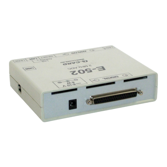
Page 10: Appearance And Main Structural Elements
1.2. Appearance and main structural elements Fig.1-2. Front view (front panel) Fig.1-3. Back view (back panel) -
Page 11: Chapter 2. Installation And Configuration
2-1) (See fig. 2-1) (See fig. 2-1) "L-Card" installs this configuration using jumpers on the board (fig. 2-1) – inside the pack. See 2.2.1 2.2.2. configuration explanation in subsection Note: How to programmatically resolve the Ethernet interface, explained in p. -
Page 12: Internal Construction Elements And E-502 Configuration
2.2. Internal construction elements and E-502 configuration. D I G I T A L +8…+30 V Технологический Technological Гальванический Galvanic разъём connector барьер barrier CPLD ADSP- JTAG BF523 Blackfin UART JTAG FPGA Cyclone Элементы ЦАП elements SDRAM LPC4337 A N A L O G Technological RESET LAN Техноло-... -
Page 13: Configuration Of The Dac Outputs Of The Connector Analog (Dac1/+15V/Agnd/Nc And Dac2/-15V/Dgnd/Nc)
2.2.1. Configuration of the DAC outputs of the connector Analog (DAC1/+15V/AGND/NC and DAC2/-15V/DGND/NC) fig. 1-1 If your modification E-502 ( ) has DAC, then "by default" the DAC within E-502 should fig. 4-3, p. 32 be connected to contacts 18 and 19 of the connector Analog ( If necessary, you can independently change the configuration of these outputs by rearranging fig. -
Page 14: Led2
E-502 failure or a sign of the heavy external electromagnetic environment in which the E-502 is located, which led to a malfunction. Contact the "L-Card" technical support if the E-502 gets into this state after turning on the power. -
Page 15: Serial Number. E-502 Version Number. Module Identification In A Multi-Module Configuration
2.6. E-502 application as a part of user programs LLC "L-Card" supports integration of its modules in the user systems. But when E-502 is included in any system, the system developer must mention in the documentation for his system the E-502 module of the "L-Card"... -
Page 16: Chapter 3. The Mechanism And Principle Of Operation Of E-502
3.1. Conventions 3.1.1. Convention on numbering In all products of the L-Card, the numbering of all physical objects (for example, channel numbers) in the description of the principle of action and design is always made from one! This agreement is completely unrelated to the encoding method in programming, where the numbers of these physical objects can be encoded from scratch or otherwise, in the context of the corresponding library function or programming language. -
Page 17: Operation Principle
JTAG (the convenience of the technology of independent access channel in the signal processor memory has been evaluated by users even in products E-440/ E14-440 by L-CARD!). Operation modes with E-502 via USB or Ethernet are alternative. E-502 uses 32 bit data words for a transmission via interfaces (in each word the data is counted with the index part). -
Page 18: Reference Frequency
3.3.1. Reference frequency – a signal reference frequency, from which the conversion processes are synchronized to the ADC, DAC, digital input and digital output. The E-502 uses a common reference frequency that synchronizes the start-up of the ADC, DAC, digital input and digital output to an accuracy of an integer division of this frequency. -
Page 19: Digital Input Channel
Interframe Межкадровая Interframe Межкадровая Кадр задержка Кадр Frame Frame delay задержка delay Номер Logical логического канала АЦП number Канал 1 Channel 1 Канал 2 Channel 2 Канал 3 Channel 3 Момент сэмплирования отсчётов данных АЦП Sampling timing of ADC data Fig. -
Page 20: E-502 Synchronization General Principle
3.3.5. E-502 synchronization general principle. fig. 3-2 shows a simplified block diagram explaining the general device of the synchronization system in E-502. E-502 synchronization system consists of two parts: primary and secondary synchronization circuits. 3.3.5.1. Primary synchronization. The primary synchronization circuit (I) according to the settings selects the corresponding external or internal source of the reference frequency, as well as the external or internal source of the start signal. -
Page 21: Fig. 3-2. Synchronization System Structure In E-502
You can find out about the availability of this functionality in the sales department of L-Card. The secondary synchronization circuit (II) is the ADC data selection circuit depending on the secondary synchronization conditions, operating exclusively against the background of the previously started clock signal from the output of the primary synchronization circuit (I), i.e. -
Page 22: Adjustment Of The Ratio Between The Time Of Setting The Signal And The Resolution For Each Adc Channel
• Automatic prohibition (stop) after entering the specified number of frames (from 1 to -1 frames) with the possibility of re-authorization (if the previously set resolution condition is repeated) without restarting the primary synchronization scheme 3.3.6. Adjustment of the ratio between the time of setting the signal and the resolution for each ADC channel. -
Page 23: Relative Switching Delays In Adc Channels
Межкадровая Interframe Межкадровая Interframe Кадр Frame задержка Кадр Frame задержка delay delay Номер ADC logical логического channel канала АЦП number Канал 1 Channel 1 Канал 2 Channel 2 Канал 3 Channel 3 Отброшенный отсчёт данных АЦП Discarded ADC data sample Момент... - Page 24 For ADC mode without averaging (n =1), the relative switching delay between adjacent ADC channels within one frame (in the order of polling the control table) is equal to t , and between the last channel of the previous frame and the first channel of the next one is t If the averaging mode is used (n >1), where n are selected equal for all ADC channels, the...
-
Page 25: Relative Delays Of The Adc, Dac And I/O Channels
3.3.8. Relative delays of the ADC, DAC and I/O channels. ST_SU CONV_OUT START_OUT ST_H X,Y, GND32 ADC_SU Выборка Выборка Sample Выборка Sample Sample Внутренний Internal 1-го отсчёта АЦП 3-го отсчёта АЦП 2-го отсчёта АЦП 1st ADC count 3rd ADC count 2nd ADC count преобразо- converter... - Page 26 Description Desig- Timing sample nation Minimum Typical Maximum Time of holding state "1" to 150 ns ST_H START_OUT after the front CONV_OUT (termination of data collection) The time to set the data at the DI input 5 ns DI_SU Data hold time at the DI input -1 ns DI_H 6 ns...
-
Page 27: Operation Principle And Function Circuit
3.4. Operation principle and function circuit LED1 Только для E-502- - -D Only for CONV_IN, START_IN Подсистема I/O sub-system Схема E-502 primary ввода-вывода первичной synchronization ЦАП DAC1, DAC2 CONV_OUT, START_OUT синхронизаци scheme и E-502 DI_SYN1, DI_SYN2 DO1...DO16 Цифровой Комму- Digital O/I Switch АЦП... - Page 28 E-502 will take place. Parallel operation from both interfaces is not supported. "L-Card" reserves the right to optionally equip the E-502 module with either the LPC4333 or LPC4337 processor without any distinctive product marking and without corresponding differences in product passports...
-
Page 29: All Functional Differences Of E-502 And L-502
3.5. All functional differences of E-502 and L-502. Functional difference L-502 E-502 Structure PCI Express card (installed External module in relation to the inside the PC) Interface with the PC PCI Express 1.0 USB 2.0 Ethernet (100BASE-TX) Intermodule Uses a different connector. Has a single Digital connector with synchronization interface digital I/O signals. -
Page 30: Chapter 4. Connection Of Signals
Chapter 4. Connection of signals. This section contains information on E-502 connectors, their contacts' purpose and main characteristics of E-502 inputs and outputs, related to the current connection. 4.1. DGND, AGND circuits AGND is a common wire circuit of isolated analog circuits: ADC inputs and DAC outputs. DGND is a common cable circuit of isolated digital circuits: digital inputs and outputs. -
Page 31: E-502 Connectors Description
Корпус Цифровые Connector Digital signals разъёма сигналы chassis (CHASSIS) (DGND) D I G I T A L Отв. 3,05 мм Port Ø3,05 mm GHASSIS Гальванический Galvanic barrier барьер CPLD ADSP- JTAG Blackfin UART BF523 (GND) (GND) JTAG ARM (GND) FPGA Cyclone Элементы... -
Page 32: Table 4-1: Connector Analog
AGND GND32 DAC1 / +15V / AGND / NC DI_SYN1 DAC2 / -15V / DGND / NC Fig. 4-3: Connector Analog Table 4-1: Connector Analog Signal name Commo Direction Description n point • Non-inverting channel voltage input 1 ... 16 for differential and X<1…16>... - Page 33 Signal name Commo Direction Description n point DAC1 AGND Output For modifications, E-502-░-░-D can be configured with a jumper as the output of the 1st channel of the DAC (voltage output in the / +15 V range -5 ... + 5 V). / AGND For any modifications, the E-502 can be configured with a jumper as + / NC...
-
Page 34: Connector Digital
4.4.2. Connector Digital. Connector Digital is a 37-pin 2-row plug of DRB-37F type on the E-502 front panel. The conductive connector contact piece (shield) is electrically connected to the GND signal ground circuit. On the shield of the cable part of the connector, the shield of the signal cable can be directly sealed. -
Page 35: Table 4-2: Connector Digital
Table 4-2: Connector Digital Commo Direc- State after Signal name Description n point tion connection DI<13…1> DGND Input Input 16-bit digital input, where DI1 is the low bit, DI16 is the high bit of the 16-bit word. The inputs DI14, DI15, DI16 are described below, they have alternative programmable functions for the synchronization inputs. - Page 36 Commo Direc- State after Signal name Description n point tion connection +3.3 V DGND Output Output Output +3.3 V supply external digital nodes. +3.3 V Short circuit of the +3.3 V circuit is undesirable, but permissible (causes heat protection of the internal stabilizer).
-
Page 37: Fig. 4-5: Synchronization Scheme Master - Slave
4.4.2.1. Connections with intermodule synchronization. fig. 4-5 fig. 4-7. Examples of connections with intermodule synchronization are shown on – Connections should be made with shortest twisted pairs for a number of E-502 modules located next to each other. The software of such a system should ensure the start of data collection of the master module after the slave starts and pre-programmed these modules to the appropriate synchronization modes. -
Page 38: Fig. 4-7: Example Of A Two-Circuit Synchronization Scheme
E-502 #4 (ведомый) (slave) Цепь 1 Цепь 2 Circuit 2 Circuit 1 E-502 #1 E-502 #3 (ведомый) E-502 #2 (slave) (ведущий) (ведомый для #1, (master) (slave for #1, master ведущий для #3, #4 ) for #3, #4) Fig. 4-7: Example of a two-circuit synchronization scheme 4.4.2.2. -
Page 39: Jtag Connectors Of Blackfin Processor
4.4.3. JTAG connectors of Blackfin processor. To debug your own Blackfin software on the E-502 board, you should use one of the JTAG- emulators from Analog Devices: ADZS-USB-ICE, ADZS-HPUSB-ICE or ADZS-ICE-100B with the USB-interface. They differ significantly with USB transfer rate and price. -
Page 40: The Maximum Allowable Conditions At The Inputs And Outputs Of Signal Lines
4.5. The maximum allowable conditions at the inputs and outputs of signal lines. Under the maximum permissible conditions are meant such currents and voltages that do not lead to failure or irreversible degradation of the characteristics of the E-502. At the same time, the maximum permissible conditions may not provide the performance characteristics of the product. -
Page 41: Adc Input Operation Voltage Range
4.6. ADC input operation voltage range Note that in the differential mode on the sub-bands ±10, ±5 V, the E-502 has unbalanced input and output ranges for the inputs X and Y with respect to the AGND analog ground circuit, and in the "common ground"... - Page 42 Отдалённая группа одноф азны х И Н Отдалённы е одноф азны е И Н и диф ф . реж им L-502 Remote single-phase VS group and "with Remote single-phase VS and diff. L-502 mode и реж им с “общ ей зем лёй” L-502 common ground"...
-
Page 43: Preconditions For Correct Connection And Correct Settings Of The Input Of The Adc E-502
4.7. Preconditions for correct connection and correct settings of the input of the ADC E-502. Simplified examples of connection of the ADC input are given in section , however, ... if you do not take into account the electrical properties of the signal sources, wires (cables) when using E-502 ADC connections, use the default E-502 program settings, then, most likely, you will get a bad result. -
Page 44: Calculation Of Total Load Power Of E-502 Output Circuits
sources and causes of these interferences (before switching to multi-channel mode and averaging mode, when it is more difficult to understand the sources of interference). 7. When using ("by default") in the multi-channel operation mode of the maximum switching frequency (2 MHz), the output impedance of the E-502 signal circuit must be from 0 to 50 Ω... - Page 45 where is the total load power taken from digital DO outputs in the "1" state (only for loads connected to the GND circuit); — power load removed from the DAC outputs; — power load, taken from the output of +15 V; —...
-
Page 46: Chapter 5. Specifications
Chapter 5. Specifications. The following specifications show the main parameters of the E-502 for its intended operating mode. For the maximum permissible voltages and currents at the contacts of the connectors, see section , on p. 5.1. ADC Parameter Value Number of channels 16 differential or 32 with "common ground"... -
Page 47: Limits Of The Permissible Relative Basic Error Of Measuring The Ac Voltage
±1 V 92 dB ±0.5 V 92 dB ±0.2 V 92 dB Resistance to overloads by input measuring signal of DC voltage ±15 V Limits of the permissible relative fundamental error of the ADC ±0.005 % conversion frequency AC voltage measurement range From 0.2 mV to 7 V 5.1.1 Limits of the permissible relative basic error of measuring the AC... -
Page 48: Adc Inter-Channel Passing
5.1.3. ADC inter-channel passing. Channel polling time, μs (with averaging factor equal to 1) or Signal source resistance channel setup time, μs (in the channel where the interchannel passage is measured) 16.0 Interchannel traversal, dB (the signal from the previous channel in the order of interrogation) 0-50 Ohm 1 kOhm... -
Page 49: Digital Inputs
± × − More than 15 to 50 incl. ± × − More than 50 to 100 incl. Note s – the final value of the range of AC voltage playback, X = 3.5 V. АС АС 2 X is the value of the voltage to be reproduced. 5.3. -
Page 50: Digital Outputs
5.4. Digital outputs. Parameter Value Number of digital outputs of general purpose Control of the third state of outputs Byte Data entry modes Synchronous, asynchronous Maximum speed in synchronous mode 1 KWords/s Maximum speed in asynchronous mode the actual speed depends on many factors of the software and hardware environment. -
Page 51: Characteristics Of Standard Interfaces
5.6. Characteristics of standard interfaces. Parameter, characteristics Value, description Interface with a computer Standards for interfaces with PC USB 2.0 100BASE-TX Bit depth of program data word 32 bits Data transmission speed • 5 Mwords/s via USB on input and output •... -
Page 52: Power Supply System And Galvanic Isolation
5.7. Power supply system and galvanic isolation. Parameter, characteristics Value, description Operating voltage range of the E-502 low- +8…+30 V voltage supply input Power consumption: • to 6 W From the external E-502 power source • From the USB input No more than 0.025 W Test voltage of galvanic isolation: •... -
Page 53: Construction Specification
5.8. Construction specification. Parameter Value Dimensions 140 x 112 x 39 mm (without cable connectors) Weight, max. 350 g (with a case, without cable connectors) 5.9. Environmental conditions. 5.9.1. Normal conditions Parameter Value Normal operating conditions: – environment temperature, °С 20±5 –... -
Page 54: Chapter 6. Connexion Samples
Chapter 6. Connexion samples. These connection examples should be considered inextricably with the recommendations for connection and settings of the E-502 (p. 4.7). The short form of information provided in this chapter does not cover all the features of the connection for your particular case. - Page 55 Forbidden to connect in this way!: X1 (X2-X16, Y1-Y16) X1 (X2-X16, Y1-Y16) X1 (X2 -X16) E-502 E-502 E-502 AGND GND32 Y1 (Y2 -Y16) X1 (X2 -X16) Y1 (Y2 -Y16) E-502 E-502 AGND AGND 6.1.1.3. Voltage divisor. 6.1.1.4. Voltage divisor. Mode "with common ground" "Differential"...
- Page 56 6.1.1.7. Closed entry. Mode "with common 6.1.1.8. Closed entry. Mode earth" "differential" С С X1 (X2 -X16) X1 (X2-X16, Y1-Y16) L-502 L-502 Y1 (Y2 -Y16) GND32 AGND AGND The connection is recommended for single-channel mode. R should be located close to E-502 input. 6.1.1.9.
-
Page 57: Connection To Adc Input With Up To 16 Differential Voltage Sources
6.1.2. Connection to ADC input with up to 16 differential voltage sources 6.1.2.1. General case X1 (X2-X16) Uвх E-502 Y1 (Y2 -Y16) AGND Only for E-502 voltage subbands: ± 2 V, ± 1 V, ± 0.5 V, ± 0.2 V. 6.1.2.2. -
Page 58: Connection To The Adc Input For The Case Where The Common Wire Of The Signal
6.1.2.4. Differential winding connection 6.1.2.5. Differential winding connection with midpoint with midpoint through the divider X1 (X2 -X16) X1 (X2 -X16) AGND AGND E-502 E-502 Y1 (Y2 -Y16) Y1 (Y2 -Y16) Locate R1 close to E-502 input. Locate R1 close to E-502 input. Only for E-502 voltage subbands: ±2 V, ±1 Only for E-502 voltage subbands: ±2 V, ±1 V, ±0.5 V, ±0.2 V... -
Page 59: Differential Connection Of The Transformer (Throttle) Winding With Midpoint And Offset Potential With Respect To Agnd
6.1.5. Differential connection of the transformer (throttle) winding with midpoint and offset potential with respect to AGND Limitations: X1 (X2 -X16) |Ucm| ≤ 1 V Only for E-502 voltage subbands: ±2 V, ±1 V, ±0.5 V, ±0.2 V E-502 Y1 (Y2 -Y16) Uсм... - Page 60 6.1.7.3. Differential mode, offset potential 6.1.7.4. Differential mode, isolated due to current source in regard to AGND current source X1 (X2 -X16) X1 (Y2 -Y16) AGND E-502 E-502 Y1 (X2-X16) Y1 (Y2 -Y16) Uсм AGND R = R1 + R2 Only for E-502 voltage subbands: ±2 V, ±1 V, ±0.5 V, ±0.2 V Fixed ADC ±...
-
Page 61: The Coordinated Connection Of Remote Sources Of Current Or Voltage Through A Long Line With A Wave Impedance Zw
6.1.8. The coordinated connection of remote sources of current or voltage through a long line with a wave impedance Zw (If the signal source has an output impedance, unequal to Zw, then these cases correspond to one-way matching of the long line on the side of the signal receiver) 6.1.8.1. -
Page 62: The Coordinated Connection Of A Remote Voltage Source Through A Pair Of Long Line With A Wave Resistance Zw With Matching On The Signal Source Side
6.1.9. The coordinated connection of a remote voltage source through a pair of long line with a wave resistance Zw with matching on the signal source side Источник Voltage напряжения source =Zв/2 ВН X1 (Y2 -Y16) R=Zв R=Zв/2 Y1 (Y2-Y16) E-502 AGND –... -
Page 63: Connecting The Dac Outputs
6.2. Connecting the DAC outputs. To carryout the DAC function in E-502-░-░-D, the outputs DAC1 and DAC2 should be 2.2.1 preconfigured with jumper, see p. 6.2.1. Mode "with common ground" 2- 6.2.2. Single-channel differential channel output ±5 V output ±10 V DAC1 DAC1 DAC2... -
Page 64: Connecting The Digital Inputs And Outputs
6.3. Connecting the digital inputs and outputs. 6.3.1. Connecting the LED or the optron input. Option 1 The LED is lit when the DO output is at the "logical DO (1-16) unit". E-502 DGND 6.3.2. Connecting the LED or the optron input. Option 2 The LED is lit when the DO output is at the "logical +3.3V zero". -
Page 65: Chapter 7. Design Data
Chapter 7. Design data 7.1. Circuit plate draft. 4 ports of Ø3.2 Note: diameter of 4 ports taking into account metallization: 3.05 mm... -
Page 66: Front Panel Draft
7.2. Front panel draft. 2 ports of Ø5.5 7.3. Back panel draft. - Page 67 List of tables. Table 4-1: Connector Analog ......................... 32 Table 4-2: Connector Digital ........................35 Table 4-3 Maximum permissible E-502 input/output conditions ............40 Table 4-4 Maximum permissible through currents by common wires circuits: ......... 40...
- Page 68 List of figures Fig. 1-1. The notation system of the E-502 module ................8 Fig.1-2. Front view (front panel)......................10 Fig.1-3. Back view (back panel) ......................10 Fig. 2-1. Internal configuration ......................12 Fig. 3-1. Illustration of the personnel principle for acquiring ADC data ..........19 Fig.
Need help?
Do you have a question about the ADC Series and is the answer not in the manual?
Questions and answers