
Related Manuals for ADLINK Technology USB-1901


Summary of Contents for ADLINK Technology USB-1901
- Page 1 USB-1900 Series 16-bit 250kS/s USB 2.0-based High-performance DAQ Module USB-1901/1902/1903 User’s Manual 2.00 Manual Rev.: Revision Date: August 31, 2011 Part No: 50-1Z084-2000 Advance Technologies; Automate the World.
-
Page 2: Revision History
Revision History Revision Release Date Description of Change(s) 2.00 Aug 31, 2011 Initial release... -
Page 3: Preface
USB-1900 Series Preface Copyright 2011 ADLINK Technology Inc. This document contains proprietary information protected by copy- right. All rights are reserved. No part of this manual may be repro- duced by any mechanical, electronic, or other means in any form without prior written permission of the manufacturer. - Page 4 Using this Manual Audience and Scope The USB-1900 Series User’s Manual is intended for hardware technicians and systems operators with knowledge of installing, configuring and operating industrial grade single board computers. Manual Organization This manual is organized as follows: Preface: Presents important copyright notifications, disclaimers, trademarks, and associated information on the proper understand- ing and usage of this document and its associated product(s).
- Page 5 USB-1900 Series Conventions Take note of the following conventions used throughout this manual to make sure that users perform certain tasks and instructions properly. Additional information, aids, and tips that help users perform tasks. NOTE: NOTE: Information to prevent minor physical injury, component dam- age, data loss, and/or program corruption when trying to com- plete a task.
- Page 6 This page intentionally left blank.
-
Page 7: Table Of Contents
USB-1900 Series Table of Contents Revision History..............ii Preface ..................iii List of Figures ................ xi List of Tables................ xiii 1 Introduction ................ 1 Overview................1 Features................1 Applications ................. 2 Specifications............... 3 1.4.1 General Specifications..........3 1.4.2 Analog Input ............... 4 1.4.3 Analog Output............. - Page 8 3 Installing the USB-1900 Series Module......31 Connecting the USB-1900 Series Module ......31 Device ID ................32 Hardware Configuration ............. 33 4 Operation ................35 Signal Function ..............35 A/D Conversion..............36 4.2.1 Analog Input Circuitry ..........37 4.2.2 AI Data Format ............
- Page 9 Mode 8: Continuous Gated Pulse Generation..62 4.8.9 Mode 9: Edge Separation Measurement....62 4.8.10 Mode 10: PWM Output ..........63 5 Calibration................. 65 Loading Calibration Constants........... 65 Auto-Calibration (USB-1901/1902 only) ......65 Saving Calibration Constants ..........66 Important Safety Instructions ..........67 Getting Service..............69...
- Page 10 This page intentionally left blank.
-
Page 11: List Of Figures
USB-1900 Series List of Figures Figure 2-1: USB-1902 Module Rear View........11 Figure 2-2: USB-1902 Module Side View ........12 Figure 2-3: USB-1902 Module Front View ........13 Figure 2-4: Module, Stand, Connector, and USB Cable ..... 14 Figure 2-5: Module, Stand, &... - Page 12 Figure 4-17: Infinite Iteration Waveform Generation ..... 55 Figure 4-18: Mode 1-Simple Gated-Event Calculation....58 Figure 4-19: Mode 2-Single Period Measurement ......59 Figure 4-20: Mode 3-Single Pulse-Width Measurement ....60 Figure 4-21: Mode 4-Single-Gated Pulse........60 Figure 4-22: Mode 5-Single-Triggered Pulse ........ 61 Figure 4-23: Mode 6-Re-Triggered Single Pulse ......
- Page 13 USB-1900 Series List of Tables Table 2-1: USB-1901/1902 pin assignment in single-end AI mode............21 Table 2-2: USB-1901/1902 pin assignment in pseudo-differential AI mode........... 22 Table 2-3: USB-1903 pin assignment ..........23 Table 2-4: CN1/CN2 I/O Signal Description........24 Table 4-1: Bipolar Analog Input Range and Output Digital Code ... 37 Table 4-2: Bipolar Output Code ............
- Page 14 This page intentionally left blank.
-
Page 15: Introduction
Introduction 1.1 Overview The USB-1900 Series of 16-bit 250 kS/s USB 2.0-based high-per- formance DAQ modules includes models USB-1901/1902, featur- ing four different voltage input ranges, and USB-1903, with additional built-in precision current-to-voltage resistors capable of direct measurement of current signal from 0 to 20 mA. -
Page 16: Applications
1.3 Applications Automotive testing Waveform generation Laboratory research Biotech measurement I/O control Introduction... -
Page 17: Specifications
USB-1900 Series 1.4 Specifications 1.4.1 General Specifications I/O Specifications Number of channels 8-CH programmable function digital input (DI) 4-CH programmable function digital output (DO) Compatibility TTL (single-end) (supports 3.3V and 5 V DI but 3.3V DO) Input voltage Logic low: VIL = 0.8 V max; IIL = 0.2 mA max.Logic high: VIH = 2.0 V min.;... -
Page 18: Analog Input
1.4.2 Analog Input Analog Input (AI) USB-1901/1902 USB-1903 General Voltage 16 single-end (SE) or 8 Number of input pseudo-differential input channels: Current (programmable) 8 differential Input A/D converter AD7610 or equivalent 250K samples/s (single channel) Maximum sampling rate 250K/N-channel samples/s (scanning) - Page 19 USB-1900 Series Analog Input (AI) USB-1901/1902 USB-1903 Electrical Offset error (gain=1) ±0.1 mV (typical) ±0.01 mA (typical) ±0.05% of FSR Gain error (gain=1) ±0.05% of FSR (typical) (typical) –3dB small signal 600 kHz bandwidth System noise 0.3 LSB CMRR 93 dB...
- Page 20 1. -3dB small signal bandwidth: (Typical, 25°C, single-ended) Input Range Bandwidth (-3dB) ± 10 V 600 kHz ± 2 V 630 kHz ± 1 V 660 kHz ± 200 mV 350 kHz 2. System Noise, SFDR, SINAD, THD, SNR (Typical, 25°C, sin- gle-ended) Input System Noise...
-
Page 21: Analog Output
USB-1900 Series 1.4.3 Analog Output Analog Output (AO) Number of channels D/A converter DAC8871 or equivalent Maximum update rage 1M samples Resolution 16 bits FIFO size 10k samples, 2-CH sharing Data transfers (bulk trans.) Programmed I/O, Continuous Output range ± 10V Output coupling Output impedance 0.01 (maximum) -
Page 22: Unpacking Checklist
1.5 Unpacking Checklist Before unpacking, check the shipping carton for any damage. If the shipping carton and/or contents are damaged, inform your dealer immediately. Retain the shipping carton and packing materials for inspection. Obtain authorization from your dealer before returning any product to ADLINK. Ensure that the fol- lowing items are included in the package. -
Page 23: Utilities For Windows
USB-1900 Series 1.7.2 DAQPilot DAQPilot is a SDK with a graphics-driven interface for various application development environments. DAQPilot represents ADLINK's commitment to full support of its comprehensive line of data acquisition products and is designed for the novice to the most experienced programmer. - Page 24 This page intentionally left blank. Introduction...
-
Page 25: Hardware Information
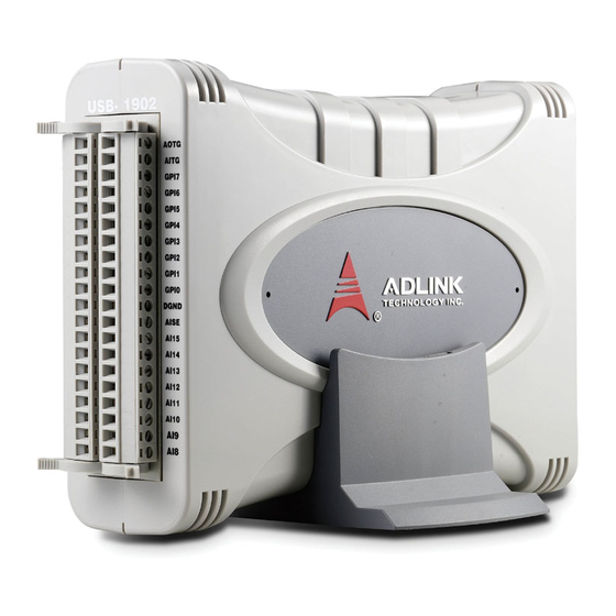
USB-1900 Series Hardware Information This chapter provides information regarding dimensions, connec- tion, accessories, and pin assignments for the USB-1900 Series. 2.1 Overview and Dimensions All dimensions shown are in millimeters (mm) While model USB-1902 is illustrated as an example, all dimensions and external features NOTE: NOTE: shown (excepting pin connections) are common... -
Page 26: Figure 2-2: Usb-1902 Module Side View
Figure 2-2: USB-1902 Module Side View Hardware Information... -
Page 27: Figure 2-3: Usb-1902 Module Front View
USB-1900 Series 41.3 Figure 2-3: USB-1902 Module Front View Hardware Information... -
Page 28: Module Stand
2.1.2 Module Stand The multi-function USB-1900 Series stand is compatible with desk, rail, or wall mounting. To fix the module in the stand, slide the module body into the stand until a click is heard. To remove the module from the stand, twist the bottom of the stand in a back-and forth motion and separate from the module. -
Page 29: Figure 2-6: Module In Stand Front View
USB-1900 Series Figure 2-6: Module in Stand Front View Hardware Information... -
Page 30: Figure 2-7: Module Stand Top View
20.4 20.4 Figure 2-7: Module Stand Top View Hardware Information... -
Page 31: Figure 2-8: Module Stand Side Cutaway View
USB-1900 Series Figure 2-8: Module Stand Side Cutaway View Figure 2-9: Module Stand Front View Hardware Information... -
Page 32: Rail Mounting
2.1.3 Rail Mounting The multi-function stand can be mounted on the DIN rail using the rail-mount kit as shown. Figure 2-10: Rail Mount Kit Figure 2-11: Module Pre-Rail Mounting Hardware Information... -
Page 33: Figure 2-12: Module Rail-Mounted
USB-1900 Series Figure 2-12: Module Rail-Mounted Hardware Information... -
Page 34: Wall Mounting
2.1.4 Wall Mounting The multi-function stand can be fixed to a wall using four flush head screws as shown. The four screw holes should be approximately 3.4 mm in diameter. 20.4 13.0 Figure 2-13: Wall Mount Holes Figure 2-14: Module with Wall Mount Apparatus Hardware Information... -
Page 35: Connector Pin Assignment
AITG GPI7 GPO3 GPI6 GPO2 GPI5 GPO1 GPI4 GPO0 GPI3 DGND GPI2 AGND GPI1 *AO1 GPI0 *AO0 DGND AGND AISE AI15 AI14 AI13 AI12 AI11 AI10 *NC for USB-1901 Table 2-1: USB-1901/1902 pin assignment in single-end AI mode Hardware Information... -
Page 36: Table 2-2: Usb-1901/1902 Pin Assignment In Pseudo-Differential Ai Mode
DGND GPI2 AGND GPI1 *AO1 GPI0 *AO0 DGND AGND AISE AIL3 AIL7 AIH3 AIH7 AIL2 AIL6 AIH2 AIH6 AIL1 AIL5 AIH1 AIH5 AIL0 AIL4 AIH0 AIH4 *NC for USB-1901 Table 2-2: USB-1901/1902 pin assignment in pseudo-differential AI mode Hardware Information... -
Page 37: Table 2-3: Usb-1903 Pin Assignment
USB-1900 Series Function Function ECLK AOTG AITG GPI7 GPO3 GPI6 GPO2 GPI5 GPO1 GPI4 GPO0 GPI3 DGND GPI2 AGND GPI1 GPI0 DGND AGND AISE CI3- CI7- CI3+ CI7+ CI2- CI6- CI2+ CI6+ CI1- CI5- CI1+ CI5+ CI0- CI4- CI0+ CI4+ Table 2-3: USB-1903 pin assignment Hardware Information... -
Page 38: Connector Signal Description
Table 2-4: CN1/CN2 I/O Signal Description 2.3 Analog Input Signal Connection The USB-1901 and 1902 provide up to 16 single-end or 8 pseudo-differential analog input channels. You can set the Chan- nel to acquire the desired input signal type combination. The ana- log signal can be converted to a digital value by the A/D converter. - Page 39 USB-1900 Series To avoid ground loops and obtain more accurate measurement from the A/D conversion, it is important to understand the type of signal source and how to choose the analog input modes from among Referenced single-end (RSE), Non-Referenced single-end (NRSE), and Pseudo-Differential Input (PDIFF).
-
Page 40: Figure 2-15: Floating Source W/ Rse Input Connections
This mode is suitable for connections with floating signal sources. When two or more floating sources are connected, these sources will be referenced to the same common ground. NOTE: NOTE: Input Multiplexer Instrumentation Amplifier Floating To A/D Signal Converter Source AIGND n = 0, ...,63 Figure 2-15: Floating source w/ RSE input connections... -
Page 41: Figure 2-16: Grnd-Referenced Sources W/ Nrse Inputs
USB-1900 Series Instrumentation Input Multiplexer x = 0, ..., 7 Amplifier Ground Referenced AIxH Signal To A/D Source Converter AIxL Common- AIGND mode noise & Ground potential Figure 2-16: GRND-Referenced Sources w/ NRSE Inputs Pseudo-Differential Input Mode Pseudo-differential input mode provides positive signal and negative signal inputs that respond to signal voltage difference between them, with the negative signal at a constant potential, as shown. -
Page 42: Figure 2-18: Floating Source W/ P-D Input
Connection of a floating signal source to the USB-1900 Series module in pseudo-differential input mode is further shown. For floating signal sources, the negative side of the signal should be connected to the AIGND, with less noise coupled into the signal connections than in single-end mode. -
Page 43: Figure 2-19: Current Input
USB-1900 Series The negative end of the differential pair is connected to the sys- tem ground after current-to-voltage conversion. 249.5 Figure 2-19: Current Input USB-1903 includes a differential amplifier in the front-end circuit providing support for common mode voltage of current source up to ±24 V. - Page 44 This page intentionally left blank. Hardware Information...
-
Page 45: Installing The Usb-1900 Series Module
USB-1900 Series Installing the USB-1900 Series Module The appropriate driver must be installed before you can con- nect the USB DAQ to your computer system. Refer to Section 1.7: Driver Support for Windows for driver support WARNING: information. 3.1 Connecting the USB-1900 Series Module 1. -
Page 46: Device Id
If the USB-1900 Series module cannot be detected, the power provided by the USB port may be insufficient. The USB-1900 Series module is exclusively powered by the USB port and requires 400 mA @ 5 V. 3.2 Device ID A rotary control on the rear of the module (as shown) controls device ID setting and can be set from 1 to 8. -
Page 47: Hardware Configuration
USB-1900 Series 3.3 Hardware Configuration remaining hardware configurations software programmable, including sampling/update rate, input/output channel, input range, and others. Please see the UD-DASK Function Reference manual for details. Installing the USB-1900 Series Module... - Page 48 This page intentionally left blank. Installing the USB-1900 Series Module...
-
Page 49: Operation
USB-1900 Series Operation Operation of the USB-1900 Series is described here to assist in configuration and programming of the module. Functions described include A/D conversion, D/A conversion, programmable function I/O, and others 4.1 Signal Function the USB-1900 Series provides 16 single-end channels or 8 pseudo-differential channels of 16-bit A/D input, and two single-end channels of 16-bit D/A output. -
Page 50: A/D Conversion
EEPROM EEPROM 24MHz XTAL Control signal DATA Cypress ADC Front end CY7C68013A 16AI 16 Bit ADC AD7610 8051 Core 12/24/48MHz FPGA DAC Circuit 16 Bit DAC DIO circuit Digital I/O, General Timer/Counter, 8DI 4DO DI DO Circuit General Timer/ Pulse Generation General Counter Timer/... -
Page 51: Analog Input Circuitry
USB-1900 Series 4.2.1 Analog Input Circuitry Analog AI[0..15] Input 16Bit ADC DATA 250ks/s AISENSE AI GND Calibration VOLTAGE FPGA Figure 4-2: Analog Input 4.2.2 AI Data Format The acquired 16-bit A/D data is 2’s complement coded data for- mat. Valid input ranges and ideal transfer characteristics are shown. -
Page 52: Software Conversion With Polling Data Transfer Acquisition Mode (Software Polling)
For current input (USB-1903), the current signal will be con- verted to voltage by a precision resistor, and the input gain fixed to 1(input range = ±10V), with transfer formula: WARNING: I (mA) = V (mV) / 24.89353693 4.2.3 Software Conversion with Polling Data Transfer Acquisition Mode (Software Polling) Generally the most convenient way to acquire a single A/D data sample, the A/D converter starts a conversion when the dedicated... -
Page 53: Figure 4-3: Analog Input Scan Timing
USB-1900 Series Continuous Scanning with Internal Hardware Timer This mode is recommended if a fixed and precise A/D sampling rate is required. You can accurately program the period between conversions of individual channels. At least four coun- ters must be specified, as follows. SI_counter (32-bit) Specify the Scan Interval = SI_counter / timebase SI2_counter (32-bit) - Page 54 Timebase Clock Source In scan acquisition mode, all A/D conversions start with the out- put of counters using the timebase as the clock source. Through the software, you can specify the timebase as the internal clock source (onboard 80 MHz). Three trigger sources are available to start the scan acquisi- tion.
-
Page 55: Analog Input Triggering
USB-1900 Series Example: 1. Set: SI2_counter = 320 SI_counter = 1280 PSC_counter = 3 NumChan_counter = 4 timebase = Internal clock source Channel entries in the Channel Gain Queue: ch1, ch2, ch0, 2. Then: Acquisition sequence of channels: 1, 2, 0, 2, 1, 2, 0, 2, 1, 2,0, 2 Sampling Interval = 320/80M s = four us Scan Interval = 1280/80M s = 16 us... -
Page 56: External Analog Triggering
4.3.2 External Analog Triggering The analog multiplexer can select one input channel as the analog trigger source. That is, one of 16 input channels in single-end mode (or 8 input channels in pseudo-differential mode) can be selected as the analog trigger source. An external analog trigger occurs when the analog trigger signal crosses above (above high) or below (below low) the pre-defined voltage level. -
Page 57: External Digital Triggering
USB-1900 Series Figure 4-5: Above-High Analog Triggering 4.3.3 External Digital Triggering An external digital trigger occurs when a rising or falling edge is detected on the digital signal connected to the AITG (analog input trigger) pin. Trigger polarity can be programmed using ADLINK software drivers. -
Page 58: Post-Trigger Acquisition Mode (No Retriggering)
4.4.1 Post-Trigger Acquisition Mode (no retriggering) Post-trigger acquisition is indicated in applications where data is to be collected after a trigger event. The number of scans for each channel after triggering is specified in the PSC_counter as shown. total acquired data length NumChan_counter... -
Page 59: Figure 4-8: Delayed Trigger
USB-1900 Series USB-1900 Series starts to acquire data. The total acquired data length = NumChan_counter * PSC_counter. When the Delay_counter clock source is set to timebase, the maximum delay time = 2 /80M s = 18.626ms WARNING: (NumChan _Counter=4, PSC_Counter=3) Trigger Scan_start AD_conversion... -
Page 60: Gated Trigger
nals occurring before the first two scans are completed will be ignored). When the re-trigger signal occurs, two more scans are performed. The process repeats until the specified number of re-trigger signals are detected. The total acquired data length = NumChan_counter * PSC_counter * Retrig_no. -
Page 61: D/A Conversion
USB-1900 Series Total acquired data length = NumChan_counter * PSC_counter. (NumChain _Counter=4, PSC_Counter=2) ACQ_EN Trigger Scan _start AD_conversion Acquisition_in_progress Acquisition Paused Acquired & Stored Data Operation Start (6 scans) Figure 4-10: Gated Trigger 4.5 D/A Conversion For complex applications, the USB-1900 Series offers software polling to update the output, and continuous mode to generate waveforms. -
Page 62: Bipolar Output Modes
4.5.1 Bipolar Output Modes The USB-1900 Series supports a maximum ±10 V voltage output. The relationship of straight binary coding between the digital codes and output voltages is as shown. Digital Code Analog Output 0x7FFF +9.999695 V (+10 V - 1 LSB) 0x0001 +0.000305 V (1 LSB) 0x0000... -
Page 63: Figure 4-11: Waveform Generation For Two Channel Update
USB-1900 Series 512 Samples Data FIFO 16 Bit Hex Data Format …… FFFF 0000 FFFE 0001 FFFD 0002 FF00 00FF Destination …… Channel Figure 4-11: Waveform Generation for Two Channel Update Data format in FIFO is shown. FFFF FFFE FFFD …………... -
Page 64: Table 4-3: Waveform Generation Timer Definition
Waveform Generation with Internal Hardware Timer Six counters interact with the waveform, generating different DAWR timings to produce various waveforms, as shown. Counter Width Description Note Update interval, defining the update Update interval = UI_counter 32-bit interval between each UI_counter / timebase* data output. -
Page 65: Waveform Trigger Sources
USB-1900 Series The maximum D/A update rate is 1 MHz, and the minimum UI_counter setting is 80. WARNING: 4 Update Count and 3 iteration count UC_Counter = 4 Trigger DAWR WF_in_Prog Delay until DLY2_Counter Delay until DLY2_Counter Delay until DLY1_Counter Reaches 0 Reaches 0 Reaches 0... -
Page 66: Waveform Generation Trigger Modes
External Digital Triggering An external digital trigger occurs when a rising edge or falling edge is detected on the digital signal connected to the AOTG (Analog output trigger) pin, as shown. Users can program the trigger polarity through ADLINK software. The signal level of the external digital trigger signals should be TTL-compatible, and the minimum pulse 20 ns. -
Page 67: Figure 4-15: Delayed-Trigger Waveform Generation
USB-1900 Series Delayed-Trigger Waveform Generation Delayed-Triggering is indicated when waveform generation is to be delayed after the trigger signal. The delay time is deter- mined by DLY1_counter, as shown. The counter calculates down on the rising edges of DLY1_counter clock source after the start trigger signal. -
Page 68: Figure 4-16: Post-Trigger Or Delayed-Trigger With Retriggering
After two trigger signals, as specified in Trig_Counter, no more trigger signals will be accepted unless a trigger reset command is executed. For more information on the Iterative Waveform Generation in this example, please see the next section. 3 update counts and 2 iterations UC_count = 3, IC_count = 2, Trig_count = 3, DLY1_count disabled, DLY2_count disabled Ignored... -
Page 69: Figure 4-17: Infinite Iteration Waveform Generation
USB-1900 Series An onboard data FIFO buffers the waveform patterns for wave- form generation. If the size of a single waveform is less than that of the FIFO, after initially loading the data from the host computer’s memory, the data in FIFO can be reused when a single waveform generation is completed and will not subse- quently occupy USB bandwidth. -
Page 70: Programmable Function I/O
In conjunction with different trigger modes and counter setups, you can manipulate a single waveform to generate different and more complex waveforms. DLY2_Counter in Iterative Waveform Generation To expand the flexibility of iterative waveform generation, the DLY2_counter separates consecutive waveform generations. The DLY2_counter starts counting down immediately following a single waveform generation. -
Page 71: General Purpose Timer/Counter
USB-1900 Series 4.6.2 General Purpose Timer/Counter The USB-1900 Series is equipped with two general purpose timer/ counter sets featuring: Count up/down controllable by hardware or software Programmable counter clock source (internal clock up to 80 MHz, external clock up to 10 MHz) Programmable gate selection (hardware or software con- trol) Programmable input and output signal polarities (high active... -
Page 72: General Purpose Timer/Counter Modes
or down (high: count up; low: count down), while the GPTC_GATE input is a control signal acting as a counter enable or counter trig- ger signal in different applications. The GPTC_OUT then gener- ates a pulse signal based on the timer/counter mode set. All input/output signal polarities can be programmed by software application. -
Page 73: Mode 2: Single Period Measurement
USB-1900 Series 4.8.2 Mode 2: Single Period Measurement The counter calculates the period of the signal on GPTC_GATE in terms of GPTC_CLK. The initial count can be loaded from the soft- ware application. After software start, the counter calculates the number of active edges on GPTC_CLK between two active edges of GPTC_GATE. -
Page 74: Mode 4: Single-Gated Pulse Generation
Software start Gate Count value Figure 4-20: Mode 3-Single Pulse-Width Measurement 4.8.4 Mode 4: Single-Gated Pulse Generation This mode generates a single pulse with programmable delay and programmable pulse-width following software start. The two pro- grammable parameters can be specified in terms of periods of the GPTC_CLK input by the software application. -
Page 75: Mode 6: Re-Triggered Single Pulse Generation
USB-1900 Series periods of the GPTC_CLK input. When the first GPTC_GATE edge triggers the single pulse, GPTC_GATE has no effect until software start is executed again. Generation of a single pulse with a pulse delay of two and a pulse-width of four is shown. Software start Gate Count value... -
Page 76: Mode 7: Single-Triggered Continuous Pulse Generation
4.8.7 Mode 7: Single-Triggered Continuous Pulse Generation This mode is similar to Mode 5 except that the counter generates contin- uous periodic pulses with programmable pulse interval and pulse-width following the first active edge of GPTC_GATE. When the first GPTC_GATE edge triggers the counter, GPTC_GATE has no effect until software start is executed again. -
Page 77: Mode 10: Pwm Output
USB-1900 Series clock frequency. The maximum counting width is 32-bit. Decrease of the counter value in Edge Separation Measurement mode is shown. S o f t w a r e s t a r t G a t e A U X C L K C o u n t v a l u e Figure 4-26: Mode 9-Edge Separation Measurement... - Page 78 This page intentionally left blank. Operation...
-
Page 79: Calibration
USB-1900 Series module in your existing testing environment, as follows. 5.2 Auto-Calibration (USB-1901/1902 only) USB-1902 auto-calibration utility measures and corrects almost all calibration errors with no external signal connections, reference voltage, or measurement devices. -
Page 80: Saving Calibration Constants
The USB-1903, requiring an external precision current source to calibrate the current-to-voltage conversion resistor and the differential buffer in its front-end circuit, does not support auto- NOTE: NOTE: calibration. Please return the module for calibration service if necessary. 5.3 Saving Calibration Constants Factory-calibrated constants are permanently stored in a bank of the onboard EEPROM and cannot be modified. -
Page 81: Important Safety Instructions
USB-1900 Series Important Safety Instructions For user safety, please read and follow all instructions, WARNINGS, CAUTIONS, and NOTES marked in this manual and on the associated equipment before handling/operating the equipment. Read these safety instructions carefully. Keep this user’s manual for future reference. Read the specifications section of this manual for detailed information on the operating environment of this equipment. - Page 82 Never attempt to fix the equipment. Equipment should only be serviced by qualified personnel. A Lithium-type battery may be provided for uninterrupted, backup or emergency power. Risk of explosion if battery is replaced with an incorrect type; please dispose of used batteries appropriately. WARNING: Equipment must be serviced by authorized technicians when:...
-
Page 83: Getting Service
Address: 5215 Hellyer Avenue, #110, San Jose, CA 95138, USA Tel: +1-408-360-0200 Toll Free: +1-800-966-5200 (USA only) Fax: +1-408-360-0222 Email: info@adlinktech.com ADLINK Technology (China) Co., Ltd. Address: (201203) 300 Fang Chun Rd., Zhangjiang Hi-Tech Park, Pudong New Area, Shanghai, 201203 China Tel: +86-21-5132-8988 Fax:... - Page 84 Address: 84 Genting Lane #07-02A, Cityneon Design Centre, Singapore 349584 Tel: +65-6844-2261 Fax: +65-6844-2263 Email: singapore@adlinktech.com ADLINK Technology Singapore Pte. Ltd. (Indian Liaison Office) Address: No. 1357, "Anupama", Sri Aurobindo Marg, 9th Cross, JP Nagar Phase I, Bangalore - 560078, India Tel: +91-80-65605817 Fax: +91-80-22443548 Email:...
Need help?
Do you have a question about the USB-1901 and is the answer not in the manual?
Questions and answers