Table of Contents
Advertisement
Quick Links
Advertisement
Table of Contents

Related Manuals for ADLINK Technology SMARC LEC-PX30


Summary of Contents for ADLINK Technology SMARC LEC-PX30
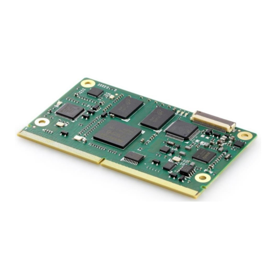
- Page 1 LEC-PX30 User’s Guide 22/01/2020 Rev. 0.7 Corrected engineering version...
- Page 3 Product names mentioned herein are used for identification purposes only and may be trademarks and/or registered trademarks of their respective companies. © Copyright 2020 ADLINK Technology Incorporated This document contains proprietary information protected by copyright. All rights are reserved. No part of this manual may be reproduced by any mechanical, electronic, or other means in any form without prior written permission of the manufacturer.
- Page 4 Caution: This information indicates the possibility of minor physical injury, component damage, data loss, and/or program corruption. Warning: This information warns of possible serious physical injury, component damage, data loss, and/or program corruption. Page 2 copyright © 2020 ADLINK Technology Inc.
- Page 5 LEC-PX30 User’s Guide SGET SMARC Rev 2.1 Revision History Revision Description Date Author Engineering version 22/8/2019 Corrected engineering version, mechanical and SMARC to controller table 6/9/2019 Page 3 copyright © 2020 ADLINK Technology Inc.
-
Page 6: Table Of Contents
SDIO ....................................................................31 4.3.10 ......................................................................... 31 4.3.11 SPI ....................................................................32 4.3.12 GPIO....................................................................33 4.3.13 UART ....................................................................34 4.3.14 CAN bus ..................................................................35 4.3.15 Miscellaneous ................................................................35 4.3.16 Power and System Management ........................................................36 Page 4 copyright © 2020 ADLINK Technology Inc. - Page 7 Yocto ....................................................................51 5.1.3 Ubuntu ................................................................... 51 6. Mechanical and Thermal ........................................................52 Module dimensions ................................................................52 Thermal Solutions ................................................................. 53 6.2.1 Heatspreader : HTS ..............................................................53 6.2.2 Heatsink : THS ................................................................54 Page 5 copyright © 2020 ADLINK Technology Inc.
- Page 8 ADLINK Technology Inc. LEC-PX30 User’s Guide List of Figures Figure 1 – Module function diagram ...................................................... 14 Figure 2 – Module top/botom side pin numbering ................................................. 15 Figure 3 – Heatspreader HTS-sPX30 ....................................................... 53 Page 6 copyright © 2020 ADLINK Technology Inc.
-
Page 9: Introduction
Carrier Boards that implement other features such as audio CODECs, touch controllers, wireless devices, etc. The modular approach allows scalability, fast time to market and upgradability while still maintaining low costs, low power and small physical size. SMARC module and carrier specifications are available online at: https://www.sget.org/standards/smarc.html Page 7 copyright © 2020 ADLINK Technology Inc. -
Page 10: Specifications
Storage for up to 16 keys, certificates or data ECDH: FIPS SP800-56A Elliptic Curve Diffie-Hellman NIST standard P256 elliptic curve support SHA-256 & HMAC hash including off-chip context save/restore AES-128: encrypt/decrypt, galois field multiply for GCM” Page 8 copyright © 2020 ADLINK Technology Inc. -
Page 11: Video
LVDS single channel 24-bit at max. 1280x800@60fps (multiplexed with MIPI DSI signal) Camera MIPI CSI RX Interface - Compatible with the MIPI Alliance Interface specification v1.0 - Up to 4 data lanes, 1.0Gbps maximum data rate per lane, supporting MIPI-HS, MIPI-LP mode Page 9 copyright © 2020 ADLINK Technology Inc. -
Page 12: Audio
Supports 10/100-Mbps data transfer rates, both full-duplex and half-duplex 2.5 Extension busses 4x USB 2.0, 1x USB OTG UART Two UART interfaces SER0 and SER2 (TX/X/CTS/RTS), 64-byte FIFO and support for 5-bit, 6-bit, 7-bit, 8-bit data transmit or receive Page 10 copyright © 2020 ADLINK Technology Inc. - Page 13 - Support for 7-bit and 10-bit address mode - Software programmable clock frequency of 100 kbit/s in Standard-mode, 400 kbit/s in the Fast-mode or 1 Mbit/s in Fast-mode Plus GPIO 12x GPIO with interrupt, one GPIO with PWM Page 11 copyright © 2020 ADLINK Technology Inc.
-
Page 14: System Storage
30-pin multipurpose flat cable connector for use with optional DB-30 debug module Provides JTAG, BMC access; UART, power test points; diagnostic LEDs, Power, Reset, Boot configuration 2.9 Power Supply Voltage 4.75 V – 5.25 V Rise Time Page 12 copyright © 2020 ADLINK Technology Inc. -
Page 15: Mechanical And Environmental
5-90% RH operating, non-condensing 5-95% RH storage (and operating with conformal coating) Shock and Vibration IEC 60068-2-64 and IEC-60068-2-27, MIL-STD-202 F, Method 213B, Table 213-I, Condition A and Method 214A, Table 214-I, Condition D Page 13 copyright © 2020 ADLINK Technology Inc. -
Page 16: Block Diagram
UART1 eMCC CAN0 CAN + FD 8/16/32/64GB SPI1 SPI0 I2S0 I2S1 PMIC I2C_PM I2C_GP Crypto Auth. ATECC608A Board Watchdog / Boot Select, Power Control Management Controller Figure 1 – Module function diagram Page 14 copyright © 2020 ADLINK Technology Inc. -
Page 17: Pinout And Signal Descriptions
The below table is a comprehensible list of all signal pins on the MXM 3 connector in the standard specification SMARC 2.1. Those signals not supported on LEC-PX30 are strikethrough STRIKETHROUGH TOP Side BOTTOM Side P156 S156 Figure 2 – Module top/botom side pin numbering Page 15 copyright © 2020 ADLINK Technology Inc. - Page 18 USB0_EN_OC# USB3_SSTX- GBE0_CTREF PCIE_D_TX+ / SERDES_1_TX+ USB0_VBUS_DET GBE0_MDI0- PCIE_D_TX- / SERDES_1_TX- USB0_OTG_ID USB3_SSRX+ GBE0_MDI0+ GBE1_LINK_ACT# USB1+ USB3_SSRX- SPI0_CS1# PCIE_D_RX+ / SERDES_1_RX+ USB1- PCIE_D_RX- / SERDES_1_RX- USB1_EN_OC# USB3+ SDIO_WP USB3- SDIO_CMD USB4+ USB2+ Page 16 copyright © 2020 ADLINK Technology Inc.
- Page 19 P136 SER2_TX S137 LVDS0_3+ / eDP0_TX3+ / DSI0_D3+ P101 HDMI_CK+ / DP1_LANE3+ S102 DP0_LANE3+ P137 SER2_RX S138 LVDS0_3- / eDP0_TX3- / DSI0_D3- P102 HDMI_CK- / DP1_LANE3- S103 DP0_LANE3- P138 SER2_RTS# S139 I2C_LCD_CK Page 17 copyright © 2020 ADLINK Technology Inc.
- Page 20 Note: STRIKETHROUGH strike-through entries are not supported functions on this product Note: Both LVDS0 and DSI0 (default) are supported, either function can be enabled at boot time in the DTS (Device Tree) Page 18 copyright © 2020 ADLINK Technology Inc.
-
Page 21: Signal Terminology Descriptions
1.8V Power Domain: Active while CARRIER_PWRON is high and CARRIER_SBY# is NOT active (i.e. both signals are high) 3.3Vsb 3.3V Power Domain: Active while CARRIER_PWRON is high (regardless of CARRIER_SBY#) 1.8Vsb 1.8V Power Domain: Active while CARRIER_PWRON is high (regardless of CARRIER_SBY#) Page 19 copyright © 2020 ADLINK Technology Inc. -
Page 22: Signal Description By Function
(either or) this will be described in the NOTES of the signal description tables by type. Note: DSI0 mode or LVDS0 can be selected at boot time through DVT (device tree), DSI0 is default Page 20 copyright © 2020 ADLINK Technology Inc. - Page 23 DDC data line used for flat panel I/O OD 1.8V Runtime PU 2k2 detection and control CMOS I2C_LCD_CK S139 DDC clock line used for flat panel O OD 1.8V Runtime PU 2k2 detection and control CMOS Page 21 copyright © 2020 ADLINK Technology Inc.
- Page 24 DDC data line used for flat panel I/O OD 1.8V Runtime PU 2k2 detection and control CMOS I2C_LCD_CK S139 DDC clock line used for flat panel O OD 1.8V Runtime PU 2k2 detection and control CMOS Page 22 copyright © 2020 ADLINK Technology Inc.
-
Page 25: Second & Third Display Interface
Note: HDMI support with a resolution of up to 1920x1080 can be implemented through a DSI to HDMI on the IPi-SMARC carrier, a reference design based on Analog Devices’ ADV7533 MIPI/DSI Receiver with HDMI Transmitter is available on request Page 23 copyright © 2020 ADLINK Technology Inc. -
Page 26: Mipi Cameras
DVT CAM1_RST# / P111 Camera 0 reset, active low output O CMOS 1.8V Runtime CAM1_PWR# is default, GPIO3 can be enabled GPIO3 through DVT CAM_MCK Master clock output O CMOS 1.8V Runtime Page 24 copyright © 2020 ADLINK Technology Inc. -
Page 27: Audio
HDA_CK CMOS Module Input if CPU acts in Slave Mode AUDIO_MCK Master clock output to I2S 1.8V Runtime codec(s) CMOS Note: I2S1 signalling has been removed during update to SMARC 2.0 specification Page 25 copyright © 2020 ADLINK Technology Inc. -
Page 28: Usb
USB over-current sense for port 2 I/O OD 3.3Vsb / Runtime PU 10k Pulled low by Module OD driver to disable USB0 power. CMOS 3.3V Pulled low by Carrier OD driver to indicate over-current situation. Page 26 copyright © 2020 ADLINK Technology Inc. - Page 29 Pulled low by Module OD driver to disable USB0 power. CMOS 3.3V Pulled low by Carrier OD driver to indicate over-current situation. Note: USB 3 & 4 ports will only be active in final design Page 27 copyright © 2020 ADLINK Technology Inc.
-
Page 30: Pcie And Serdes Pin Sharing
ADLINK Technology Inc. LEC-PX30 User’s Guide 4.3.6 PCIe and SerDes pin sharing 4.3.6.1 PCIe Ports This design does not support PCIe ports 4.3.7 SATA This design does not support SATA ports Page 28 copyright © 2020 ADLINK Technology Inc. -
Page 31: Lan
Twisted pair signals for external GBE1_MDI0- Interface Differential Pairs 0, 1. The MDI can operate in transformer. GBE1_MDI1+ 100, and 10Mbit/sec modes. GBE1_MDI1- GBE1_MDI2+ GBE1_MDI2- MDI[0]+/- TX+/- TX+/- GBE1_MDI3+ MDI[1]+/- RX+/- RX+/- GBE1_MDI3- Page 29 copyright © 2020 ADLINK Technology Inc. - Page 32 Center-Tap reference voltage for Carrier board Ethernet Analog 0 to 3.3V Runtime magnetic `(if required by the Module GBE PHY)` GBE1_SDP IEEE 1588 Trigger Signal. For hardware implementation 3.3V Runtime of PTP (precision time protocol) CMOS Page 30 copyright © 2020 ADLINK Technology Inc.
-
Page 33: Sdio
SDIO Power Enable. This signal is used to 3.3V Runtime should be driven low in STB Mode by the enable the power being supplied to a SD/MMC card CMOS module device. 4.3.10 Page 31 copyright © 2020 ADLINK Technology Inc. -
Page 34: Spi
Note: SPI0 is free to use on the carrier but support only one device through CS0 SPI1 supports a CAN bus controller on the module through CS0, that leaves CS1 free for a device on the carrier Page 32 copyright © 2020 ADLINK Technology Inc. -
Page 35: Gpio
Runtime PU 470K on the advised as INT signal to I2C GPIO expander on carrier. CMOS Module GPIO13 S123 General purpose I/O pin 13 1.8V Runtime PU 470K on the CMOS Module Page 33 copyright © 2020 ADLINK Technology Inc. -
Page 36: Uart
"Clear to Send" handshake line for port 2 1.8V Runtime CMOS SER3_TX P140 Asynchronous serial data output port 3 1.8V Runtime CMOS SER3_RX P141 Asynchronous serial data input port 3 1.8V Runtime CMOS Page 34 copyright © 2020 ADLINK Technology Inc. -
Page 37: Can Bus
Watch-Dog-Timer Output, low active. 1.8V Runtime Driven only during runtime CMOS PWM_OUT P113 Pulse Width Modulation (PWM) 1.8V Runtime PU 470K on the GPIO5 is the default pin configuration / GPIO5 output CMOS Module Page 35 copyright © 2020 ADLINK Technology Inc. -
Page 38: Power And System Management
Power-button input from Carrier board. Carrier to I OD Standby PU 10K Driven by OD on Carrier. float the line in in-active state. Active low, level CMOS Pulled up on module. sensitive. Should be debounced on the Module. Page 36 copyright © 2020 ADLINK Technology Inc. - Page 39 Standby PU 2.2K On x86 systems these serve as SMB CMOS CLK. Pulled up on module. SMB_ALERT_1V8# SMBus Alert# (interrupt) signal I OD Standby PU 2.2K only used on x86 design CMOS Page 37 copyright © 2020 ADLINK Technology Inc.
-
Page 40: Boot Select
SOC native Force Recovery mode – such as over a Serial Port. For x86 systems this signal may be used to load BIOS defaults. Pulled up on Module. Driven by OD part on Carrier. Page 38 copyright © 2020 ADLINK Technology Inc. -
Page 41: Power
P Not defined within Signal [2 to 3.25] / 3.25V power – 3.0V nominal. May be Terminolgy Descriptions. sourced from a Carrier based Should we define a specific Lithium cell or Super Cap. rail? Page 39 copyright © 2020 ADLINK Technology Inc. -
Page 42: Smarc Pin To Controller Mapping
PX30 MIPI_CSI_DP3 VCC_1V0 CSI1_RX3- PX30 MIPI_CSI_DN3 VCC_1V0 GBE0_MDI3- GBE0_MDI3+ GBE0_LINK100# Out/OD DP83822 LED_1 VCC3V3_SYS GBE0_LINK1000# GBE0_MDI2- GBE0_MDI2+ GBE0_LINK_ACT# Out/OD DP83822 LED_0 VCC3V3_SYS GBE0_MDI1- Bi-Dir DP83822 RD_M 3.3VA1 GBE0_MDI1+ Bi-Dir DP83822 RD_P 3.3VA1 Page 40 copyright © 2020 ADLINK Technology Inc. - Page 43 ESPI_CK / SPI1_CK CMOS/ VDD_IO PX30 SPI1_CLK ALT2/ALT2 VCC1V8_DVP ESPI_IO_1 / SPI1_DIN CMOS/ VDD_IO PX30 SPI1_MISO ALT2/ALT2 VCC1V8_DVP ESPI_IO_0 / SPI1_DO CMOS/ VDD_IO PX30 SIP1_MOSI ALT2/ALT2 VCC1V8_DVP USB0+ Bi-Dir PX30 OTG_DP USB_AVDD Page 41 copyright © 2020 ADLINK Technology Inc.
- Page 44 PRTCTL3 +3.3V RSVD RSVD USB3_EN_OC# PU-10K CMOS/ VDD_IO LAN9514 PRTCTL4 +3.3V PCIE_A_RST# USB4_EN_OC# PU-10K CMOS/ VDD_IO LAN9514 PRTCTL5 +3.3V PCIE_B_CKREQ# PCIE_A_CKREQ# PCIE_C_REFCK+ PCIE_C_REFCK- PCIE_A_REFCK+ PCIE_A_REFCK- PCIE_A_RX+ PCIE_A_RX- PCIE_A_TX+ PCIE_A_TX- HDMI_D2+ / DP1_LANE0+ Page 42 copyright © 2020 ADLINK Technology Inc.
- Page 45 PX30 I2C0_SCL ALT6/ALT6 VCC_1V8 P122 I2C_PM_DAT Bi-Dir PU-2k2 CMOS/ VDD_IO PX30 I2C0_SDA ALT6/ALT6 VCC_1V8 P123 BOOT_SEL0# PU-4k7 CMOS/ VDD_IO +1V8SMC P124 BOOT_SEL1# PU-4k7 CMOS/ VDD_IO +1V8SMC P125 BOOT_SEL2# PU-4k7 CMOS/ VDD_IO +1V8SMC Page 43 copyright © 2020 ADLINK Technology Inc.
- Page 46 P145 CAN1_TX P146 CAN1_RX P147 VDD_IN P148 VDD_IN P149 VDD_IN P150 VDD_IN P151 VDD_IN P152 VDD_IN P153 VDD_IN P154 VDD_IN P155 VDD_IN P156 VDD_IN CSI1_TX+ / I2C_CAM1_CK CMOS/ VDD_IO PX30 I2C2_SCL VCC_RMII Page 44 copyright © 2020 ADLINK Technology Inc.
- Page 47 VCC3V3_SYS GBE1_MDI1+ Bi-Dir LAN9514 GBE1_MDI1- Bi-Dir LAN9514 GBE1_LINK1000# GBE1_MDI2+ GBE1_MDI2- GBE1_MDI3+ GBE1_MDI3- GBE1_CTREF PCIE_D_TX+ / SERDES_1_TX+ PCIE_D_TX- / SERDES_1_TX- GBE1_LINK_ACT# Out/OD LAN9514 nLNKA_LED ALT1/ALT1 VCC3V3_SYS PCIE_D_RX+ / SERDES_1_RX+ PCIE_D_RX- / SERDES_1_RX- Page 45 copyright © 2020 ADLINK Technology Inc.
- Page 48 I2S0_2CH_LRCK_TXRX VCC1V8_DVP HDA_SDO / I2S2_SDOUT PX30 I2S0_2CH_SDO VCC1V8_DVP HDA_SDI / I2S2_SDIN PX30 I2S0_2CH_SDI VCC1V8_DVP HDA_CK / I2S2_CK Bi-Dir PX30 I2S0_2CH_SCKL VCC1V8_DVP SATA_ACT# USB5_EN_OC# ESPI_IO_2 ESPI_IO_3 ESPI_RESET# USB5+ USB5- USB3_SSTX+ USB3_SSTX- USB3_SSRX+ USB3_SSRX- Page 46 copyright © 2020 ADLINK Technology Inc.
- Page 49 USBDM4 USB2_SSTX+ USB2_SSTX- USB2_SSRX+ USB2_SSRX- PCIE_B_RST# PCIE_C_RST# PCIE_C_RX+ / SERDES_2_RX+ PCIE_C_RX- / SERDES_2_RX- PCIE_C_TX+ / SERDES_2_TX+ PCIE_C_TX- / SERDES_2_TX- PCIE_B_REFCK+ PCIE_B_REFCK- PCIE_B_RX+ PCIE_B_RX- PCIE_B_TX+ PCIE_B_TX- DP0_LANE0+ DP0_LANE0- DP0_AUX_SEL DP0_LANE1+ DP0_LANE1- DP0_HPD DP0_LANE2+ Page 47 copyright © 2020 ADLINK Technology Inc.
- Page 50 S118 LVDS1_2- / eDP1_TX2- / DSI1_D2- S119 S120 LVDS1_3+ / eDP1_TX3+ / DSI1_D3+ S121 LVDS1_3- / eDP1_TX3- / DSI1_D3- S122 LCD1_BKLT_PWM S123 GPIO13 Bi-Dir Serial-33R CMOS/ VDD_IO PX30 GPIO3_A0_d ALT1/ALT1 VCC1V8_DVP S124 Page 48 copyright © 2020 ADLINK Technology Inc.
- Page 51 / DSI0_TE S145 WDT_TIME_OUT# CMOS/ VDD_IO +1V8SMC S146 PCIE_WAKE# S147 VDD_RTC S148 LID# PU-4.7K CMOS/ VDD_IO ALT5/ALT5 +1V8SMC S149 SLEEP# PU-4.7K CMOS/ VDD_IO PX30 GPIO1_C4_u ALT5/ALT5 VCC_1V8 S150 VIN_PWR_BAD# PU-10K CMOS/ VDD_IO +1V8SMC Page 49 copyright © 2020 ADLINK Technology Inc.
- Page 52 ADLINK Technology Inc. LEC-PX30 User’s Guide S151 CHARGING# PU-68K CMOS/ VDD_IO PX30 GPIO1_C5_d ALT5/ALT5 VCC_1V8 S152 CHARGER_PRSNT# PU-100K CMOS/ VDD_IO PX30 GPIO1_C6_u ALT5/ALT5 VCC_1V8 S153 CARRIER_STBY# CMOS/ VDD_IO +1V8SMC Page 50 copyright © 2020 ADLINK Technology Inc.
-
Page 53: Software Support
LEC-PX30 User’s Guide SGET SMARC Rev 2.1 5. Software Support 5.1.1 Early Access 5.1.2 Yocto 5.1.3 Ubuntu Page 51 copyright © 2020 ADLINK Technology Inc. -
Page 54: Mechanical And Thermal
ADLINK Technology Inc. LEC-PX30 User’s Guide 6. Mechanical and Thermal 6.1 Module dimensions Page 52 copyright © 2020 ADLINK Technology Inc. -
Page 55: Thermal Solutions
LEC-PX30 User’s Guide SGET SMARC Rev 2.1 6.2 Thermal Solutions 6.2.1 Heatspreader : HTS M3 x 4pcs 2.7mm x 4pcs Figure 3 – Heatspreader HTS-sPX30 Page 53 copyright © 2020 ADLINK Technology Inc. -
Page 56: Heatsink : Ths
ADLINK Technology Inc. LEC-PX30 User’s Guide 6.2.2 Heatsink : THS 2.7mm x 4pcs Figure 4 – Heatsink THS-sPX30 Page 54 copyright © 2020 ADLINK Technology Inc. - Page 57 LEC-PX30 User’s Guide SGET SMARC Rev 2.1 Page 55 copyright © 2020 ADLINK Technology Inc.
Need help?
Do you have a question about the SMARC LEC-PX30 and is the answer not in the manual?
Questions and answers