
Related Manuals for ADLINK Technology USB-1210


Summary of Contents for ADLINK Technology USB-1210
- Page 1 USB-1210 4-CH 16-Bit 2MS/s Simultaneous-Sampling USB DAQ Module User’s Manual 2.00 Manual Rev.: Revision Date: July 31, 2014 Part No: 50-1Z162-1000 Advance Technologies; Automate the World.
-
Page 2: Revision History
Revision History Revision Release Date Description of Change(s) 2.00 July 31, 2014 Initial Release... -
Page 3: Preface
USB-1210 Preface Copyright 2014 ADLINK Technology, Inc. This document contains proprietary information protected by copy- right. All rights are reserved. No part of this manual may be repro- duced by any mechanical, electronic, or other means in any form without prior written permission of the manufacturer. - Page 4 Conventions Take note of the following conventions used throughout this manual to make sure that users perform certain tasks and instructions properly. Additional information, aids, and tips that help users perform tasks. NOTE: NOTE: Information to prevent minor physical injury, component dam- age, data loss, and/or program corruption when trying to com- plete a task.
-
Page 5: Table Of Contents
Driver Support for Windows..........14 1.10 Utilities for Windows ............14 2 Getting Started ..............15 Unpacking Checklist ............15 Attaching the Module Stand..........15 Rail Mounting..............16 Wall Mounting ..............17 Installing the USB-1210 Module ........18 Table of Contents... - Page 6 2.5.1 Connecting the USB-1210 Module ......18 2.5.2 Device ID ..............19 2.5.3 Hardware Configuration..........20 3 Operation & Calibration............ 21 Operation ................21 3.1.1 Signal Function ............21 3.1.2 A/D Conversion............22 3.1.3 Trigger Sources ............25 3.1.4 Trigger Modes............27 3.1.5...
-
Page 7: List Of Figures
Figure 2-4: Wall Mount Holes ............. 17 Figure 2-5: Module with Wall Mount Apparatus ......18 Figure 2-6: USB-1210 module in Windows Device Manager..19 Figure 2-7: Device ID Selection Control........20 Figure 3-1: Carrier Board Functional Block Diagram ....21 Figure 3-2: Daughter Board Functional Block Diagram .... - Page 8 Figure 3-20: Mode 7-Single-Triggered Continuous Pulse..... 37 Figure 3-21: Mode 8-Continuous Gated Pulse......37 Figure 3-22: Mode 9-Edge Separation Measurement....38 Figure 3-23: Mode 10-PWM Output Following Trigger ....38 Figure 3-24: Mode 10-PWM Output Following GATE Control ..38 Figure 3-25: Isolation ..............
- Page 9 USB-1210 List of Tables Table 1-1: USB-1210 Pin Assignment ..........11 Table 1-2: CN1/CN2 I/O Signal Description........12 Table 3-1: Bipolar Analog Input Range and Output Digital Code ... 23 Table 3-2: Pin Definition of LVTTL Digital I/O ......... 31 Table 3-3: Timer/Counter Pin Definition..........
- Page 10 This page intentionally left blank. List of Tables...
-
Page 11: Introduction
The USB-1210 is a 16-bit high-speed USB 2.0-based DAQ mod- ule equipped with 4 analog input channels providing simultaneous sampling at up to 2MS/s per channel. The USB-1210 delivers high accuracy and excellent dynamic performance at maximum sam- pling rates and features flexible trigger function. In addition, onboard 256MS FIFO ensures no data loss during acquisition even with heavy loading on CPU or system. -
Page 12: Specifications
1.4 Specifications 1.4.1 General Specifications Digital I/O Specifications Number of channels 8-CH programmable function digital input (DI) 4-CH programmable function digital output (DO) Compatibility LVTTL (single-end) (supports 3.3V and 5 V DI but 3.3V DO) Input voltage Logic low: VIL = 0.8 V max; IIL = 0.2 mA max.Logic high: VIH = 2.0 V min.;... -
Page 13: Analog Input
USB-1210 1.4.2 Analog Input Resolution 16 bit Channels 4 differential (simultaneous sampling) Maximum sampling rate 2MS/s per channel Programmable gain 1, 5 Input range (voltage) ± 10 V, ± 2 V ± 1mV (gain=1) Offset error ± 0.2mV (gain=5) Typical: ± 0.01% of FSR (gain=1 & 5) Gain error Maximum: ±... -
Page 14: Schematics
Programmed I/O, continuous (USB bulk Data transfer transfer mode) 1.5 Schematics All units are in millimeters (mm) NOTE: NOTE: 1.5.1 Module Figure 1-1: USB-1210 Module Rear View Introduction... -
Page 15: Figure 1-2: Usb-1210 Module Side View
USB-1210 156.5 Figure 1-2: USB-1210 Module Side View Introduction... -
Page 16: Figure 1-3: Usb-1210 Module Front View
41.3 Figure 1-3: USB-1210 Module Front View Introduction... -
Page 17: Module Stand
USB-1210 1.5.2 Module Stand The multi-function USB-1210 stand is compatible with desk, rail, or wall mounting. To fix the module in the stand, slide the module body into the stand until a click is heard. To remove the module from the stand, twist the bottom of the stand in a back-and forth motion and separate from the module. -
Page 18: Figure 1-5: Module, Stand, & Wall Mount Kit Side View (W/ Connections)
200.1 169.4 156.5 Figure 1-5: Module, Stand, & Wall Mount Kit Side View (w/ connections) 114.30 Figure 1-6: Module in Stand Front View Introduction... -
Page 19: Figure 1-7: Module Stand Top View
USB-1210 20.4 20.4 Figure 1-7: Module Stand Top View Introduction... -
Page 20: Figure 1-8: Module Stand Side Cutaway View
Figure 1-8: Module Stand Side Cutaway View Figure 1-9: Module Stand Front View Introduction... -
Page 21: Connector Pin Assignment
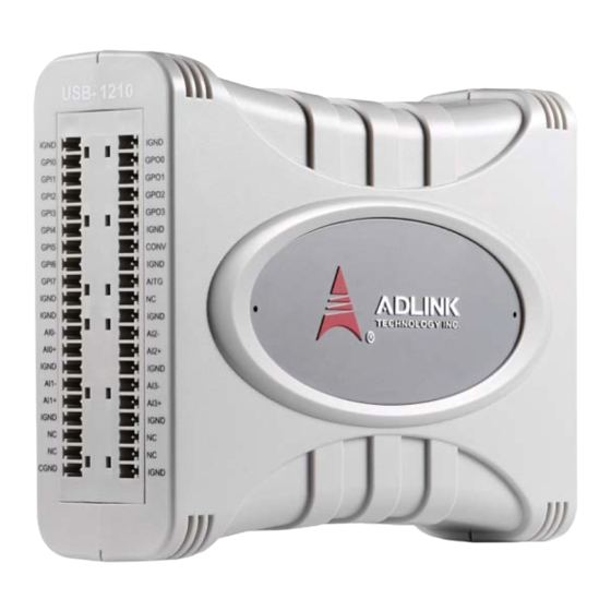
USB-1210 1.6 Connector Pin Assignment The USB-1210 module is equipped with 40-pin removable screw-down terminal connectors, with pin assignment as shown. IGND IGND GPI0 GPO0 GPI1 GPO1 GPI2 GPO2 GPI3 GPO3 GPI4 IGND GPI5 CONV GPI6 IGND GPI7 AITG IGND... -
Page 22: Analog Input Signal Connection
Table 1-2: CN1/CN2 I/O Signal Description 1.7 Analog Input Signal Connection The USB-1210 provides 4 truly differential analog input channels. These four channels are simultaneous-sampling and support up to 2MS/s per channel. The analog signal can be converted to a digi- tal value by the A/D converter. -
Page 23: Figure 1-10: Grnd-Referenced Source W/ Diff Input
IGND Figure 1-10: GRND-Referenced Source w/ DIFF Input Connection of a floating signal source to the USB-1210 module in differential input mode is further shown. For floating signal sources, the negative side of the signal should be connected to the AIGND, with less noise coupled into the signal connections than in single-end mode. -
Page 24: Software Support
LabVIEW and MATLAB . All software options are included in the ADLINK All-in-One CD. Be sure to install the driver & utility before using the USB-1210 module. 1.9 Driver Support for Windows UD-DASK UD-DASK is composed of advanced 32/64-bit kernel drivers and SDK for customized DAQ application development. -
Page 25: Getting Started
User’s manual 2.2 Attaching the Module Stand The multi-function USB-1210 stand is compatible with desk, rail, or wall mounting. To fix the module in the stand, slide the module body into the stand until a click is heard. To remove the module from the stand, twist the bottom of the stand in a back-and forth motion and separate from the module. -
Page 26: Rail Mounting
2.3 Rail Mounting The multi-function stand can be mounted on the DIN rail using the rail-mount kit as shown. Figure 2-1: Rail Mount Kit Figure 2-2: Module Pre-Rail Mounting Getting Started... -
Page 27: Wall Mounting
USB-1210 Figure 2-3: Module Rail-Mounted 2.4 Wall Mounting The multi-function stand can be fixed to a wall using four flush head screws as shown. The four screw holes should be approximately 3.4 mm in diameter. 20.4 13.0 Figure 2-4: Wall Mount Holes... -
Page 28: Installing The Usb-1210 Module
2.5.1 Connecting the USB-1210 Module 1. Turn on your computer. 2. Connect the USB-1210 module to one USB 2.0 port on your computer using the included USB cable. 3. The first time the USB-1210 module is connected, a New Hardware message appears. It will take around 6 sec- onds to load the firmware. -
Page 29: Device Id
Figure 2-6: USB-1210 module in Windows Device Manager If the USB-1210 module cannot be detected, the power provided by the USB port may be insufficient. The USB-1210 module is exclusively powered by the USB port and requires 460 mA @ 5 V. -
Page 30: Hardware Configuration
type is connected, each must be set to a different ID to avoid con- flicts and errors in operation. Figure 2-7: Device ID Selection Control 2.5.3 Hardware Configuration remaining hardware configurations software programmable, including sampling/update rate, input/output channel, input range, and others. Please see the UD-DASK Function Reference manual for details. -
Page 31: Operation & Calibration
USB-1210 Operation & Calibration Operation of the USB-1210 is described here to assist in configuration and programming of the module. Functions described include A/D conversion, programmable function I/O, and others 3.1 Operation 3.1.1 Signal Function USB-1210 provides truly differential simultaneous-sampling analog input channels of 16-bit A/D input. -
Page 32: A/D Conversion
AI CH0+ Signal DC path/ 2nd-order 1st CH AI CH0- Protection Calibration Source SDO_CH0 BUSY_CH0 SDO_CH1 AI CH1+ BUSY_CH1 AI CH1- Four channels SDO_CH2 Calibration BUSY_CH2 Mux and Reference Src AI CH2+ SDO_CH3 BUSY_CH3 AI CH2- 4th CH AI CH3+ Signal DC path/ 2nd-order... -
Page 33: Figure 3-3: Analog Input
USB-1210 Analog Input Circuitry 2 MHz ADCONV_CHn Buffer 2nd order Path Selection With Path_DC With level shift x1 or x4 Calibration SRC x1/2 AI CHx_P Signal Input AI CHx_N Signal Input Buffer Figure 3-3: Analog Input AI Data Format The acquired 16-bit A/D data is 2’s complement coded data for- mat. - Page 34 Continuous A/D Conversion Clock Source When the onboard ADC receives a conversion clock signal, A/D conversion is triggered. The USB-1210 conversion clock may originate with the internal hardware timer or externally via CONV (external A/D conversion clock) pin. While the conver-...
-
Page 35: Trigger Sources
DC to 2 MHz and the minimum pulse width is 225ns. Analog Input Triggering The USB-1210 supports flexible trigger sources for analog input functionality. The trigger source can originate with software com- mand, external analog, or external digital signal in continuous ana- log input mode. -
Page 36: Figure 3-5: Below-Low Analog Triggering
trigger occurs when the analog trigger signal crosses above (above high) or below (below low) the pre-defined voltage level. The range of trigger level is the full-scale range of the selected input channel and the resolution is 16-bit. Below-Low Analog Triggering In below-low analog triggering, as shown, the trigger signal is generated when the input analog signal is less than the Low_Threshold voltage. -
Page 37: Trigger Modes
USB-1210 Figure 3-6: Above-High Analog Triggering External Digital Triggering An external digital trigger occurs when a rising or falling edge is detected on the digital signal connected to the AITG (analog input trigger) pin. Trigger polarity can be programmed using ADLINK software drivers. -
Page 38: Figure 3-8: Post Trigger Without Retriggering
Post-Trigger Acquisition Mode (no retriggering) Post-trigger acquisition is indicated when data is to be collected after the trigger event, as shown.. Operation Trigger event occurs Acquisition stops initiates Acquisition begins Data transfer to system commences Time Trigger Data N samples Figure 3-8: Post Trigger without Retriggering Delayed-Trigger Acquisition Mode (no retriggering) Delay-trigger acquisition is indicated when the data collection is to... -
Page 39: Figure 3-10: Middle Trigger
USB-1210 Operation initiates Acquisition stops Trigger event occurs Acquisition initiates Data transfer to system begins Time Trigger Data M samples N samples Figure 3-10: Middle Trigger Pre-Trigger Mode Pre-trigger acquisition is indicated when data is to be collected before the trigger event. Acquisition commences once specified function calls are executed to begin the pre-trigger operation, and stops when the trigger event occurs. -
Page 40: Figure 3-12: Post Trigger With Retriggering
USB-1210 awaits the next re-trigger signal (re-trigger signals occurring before the N samples are completed will be ignored). When the re-trigger signal occurs, another N samples are performed. The process repeats until the specified number of re-trigger signals are detected. -
Page 41: Programmable Function I/O
*Not used in DI/O Table 3-2: Pin Definition of LVTTL Digital I/O General Purpose Timer/Counter The USB-1210 is equipped with two general purpose timer/coun- ter sets featuring: Count up/down controllable by hardware or software Programmable counter clock source (internal clock up to 80 MHz, external clock up to 10 MHz) Operation &... -
Page 42: Basic Timer/Counter Function
Programmable gate selection (hardware or software con- trol) Programmable input and output signal polarities (high active or low active) Initial Count loaded from a software application Current count value readable by software without affecting circuit operation. IGND IGND GPTC_CLK GPTC_OUT0 GPTC_UD0 GPTC_OUT1 GPTC_GATE0... -
Page 43: General Purpose Timer/Counter Modes
USB-1210 All input/output signal polarities can be programmed by software application. For brevity, all GPTC_CLK, GPTC_GATE, and GPTC_OUT in the following illustrations are assumed to be active high or rising-edge triggered. 3.1.7 General Purpose Timer/Counter Modes Ten programmable timer/counter modes are available. All modes initialize following a software-start signal set by the software. -
Page 44: Figure 3-15: Mode 2-Single Period Measurement
of GPTC_GATE. After the completion of the period interval on GPTC_GATE, GPTC_OUT outputs high and then current count value can be read by the software application. Operation in which initial count = 0, count-up mode is shown. Software start Gate Count value Figure 3-15: Mode 2-Single Period Measurement Mode 3: Single Pulse-Width Measurement... -
Page 45: Figure 3-16: Mode 3-Single Pulse-Width Measurement
USB-1210 Figure 3-16: Mode 3-Single Pulse-Width Measurement Mode 4: Single-Gated Pulse Generation This mode generates a single pulse with programmable delay and programmable pulse-width following software start. The two pro- grammable parameters can be specified in terms of periods of the GPTC_CLK input by the software application. -
Page 46: Figure 3-18: Mode 5-Single-Triggered Pulse
Software start Gate Count value Figure 3-18: Mode 5-Single-Triggered Pulse Mode 6: Re-Triggered Single Pulse Generation This mode is similar to Mode 5 except that the counter generates a pulse following every active edge of GPTC_GATE. After soft- ware start, every active GPTC_GATE edge triggers a single pulse with programmable delay and pulse width. -
Page 47: Figure 3-20: Mode 7-Single-Triggered Continuous Pulse
USB-1210 S o f t w a r e s t a r t G a t e C L K C o u n t v a l u e O U T Figure 3-20: Mode 7-Single-Triggered Continuous Pulse... -
Page 48: Figure 3-22: Mode 9-Edge Separation Measurement
C o u n t v a l u e Figure 3-22: Mode 9-Edge Separation Measurement Mode 10: PWM Output The USB-1210 timer/counter can also simulate a PWM (Pulse Width Modulation) output. The PWM starts to generate output fol- lowing a GPTC_GATE edge trigger or being activated/inactivated by the GPTC_GATE high/low logic control. -
Page 49: Isolation
Pulse length 3.1.8 Isolation The USB-1210 provides 500VDC isolation capability to protect against hazardous voltage caused by erroneous signal connection or signal levels to be measured exceeding expectation. The isola- tion circuit can also reduce the ground-loop noise. DDR3... -
Page 50: Auto-Calibration
EEPROM. When auto-calibration is complete, the new calibration constants can be saved to the user-configurable banks in the EEPROM. The USB-1210 should be warmed up for at least 15 minutes before initiating auto-calibration NOTE: NOTE: Operation &... -
Page 51: Important Safety Instructions
USB-1210 Important Safety Instructions For user safety, please read and follow all instructions, WARNINGS, CAUTIONS, and NOTES marked in this manual and on the associated equipment before handling/operating the equipment. Read these safety instructions carefully. Keep this user’s manual for future reference. - Page 52 Never attempt to fix the equipment. Equipment should only be serviced by qualified personnel. A Lithium-type battery may be provided for uninterrupted, backup or emergency power. Risk of explosion if battery is replaced with an incorrect type; please dispose of used batteries appropriately. WARNING: Equipment must be serviced by authorized technicians when:...
-
Page 53: Getting Service
San Jose, CA 95138, USA Tel: +1-408-360-0200 Toll Free: +1-800-966-5200 (USA only) Fax: +1-408-360-0222 Email: info@adlinktech.com ADLINK Technology (China) Co., Ltd. Address: (201203) 300 Fang Chun Rd., Zhangjiang Hi-Tech Park Pudong New Area, Shanghai, 201203 China Tel: +86-21-5132-8988 Fax: +86-21-5132-3588 Email: market@adlinktech.com... - Page 54 84 Genting Lane #07-02A, Cityneon Design Centre Singapore 349584 Tel: +65-6844-2261 Fax: +65-6844-2263 Email: singapore@adlinktech.com ADLINK Technology Singapore Pte. Ltd. (Indian Liaison Office) Address: #50-56, First Floor, Spearhead Towers Margosa Main Road (between 16th/17th Cross) Malleswaram, Bangalore - 560 055, India Tel: +91-80-65605817, +91-80-42246107 Fax:...
Need help?
Do you have a question about the USB-1210 and is the answer not in the manual?
Questions and answers