Table of Contents
Advertisement
Page 1 of 35
Genesys 2 Reference Manual
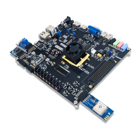
The Digilent Genesys 2 board is an advanced, high-performance, ready-to-use digital circuit development platform based on
the latest Kintex-7™ Field Programmable Gate Array (FPGA) from Xilinx. With its high-capacity, high-speed FPGA (Xilinx
part number XC7K325T-2FFG900C), fast external memories, high-speed digital video ports, and wide expansions options
make the Genesys 2 well suited for data and video processing applications. Several built-in peripherals, including Ethernet,
audio and USB 2.0, allow a wide range of other applications. The fully-bonded high-speed FMC HPC connector opens the
1)
door to great expansion possibilities.
Advertisement
Table of Contents

Related Manuals for Digilent Genesys 2


Summary of Contents for Digilent Genesys 2
- Page 1 XC7K325T-2FFG900C), fast external memories, high-speed digital video ports, and wide expansions options make the Genesys 2 well suited for data and video processing applications. Several built-in peripherals, including Ethernet, audio and USB 2.0, allow a wide range of other applications. The fully-bonded high-speed FMC HPC connector opens the...
- Page 2 Page 2 of 35...
- Page 3 Page 3 of 35...
- Page 4 Page 4 of 35...
- Page 5 • Two four-lane DisplayPort connectors • HDMI Sink and HDMI Source • 10/100/1000 Ethernet PHY • 1GiB 1800Mt/s on-board DDR3 • USB 2.0 Host/Device/OTG PHY • Digilent Adept USB port for programming and data • Ten GTX lanes available in the FMC connector...
- Page 6 The Genesys 2 is compatible with Xilinx’s new high-performance Vivado® Design Suite as well as the ISE toolset. Included in the box is a voucher that unlocks the Design Edition of Vivado that is device-locked to the Genesys 2. This allows designs to be implemented straight out of the box at no additional cost.
-
Page 7: Quick Start
1. Quick-start The Genesys 2 comes with an out-of-box demo design that gets loaded from the on-board QSPI flash. It exercises most of the on-board peripherals. Just power the board with the included 12V wall supply, flick the power switch, wait for the design to... -
Page 8: Power Supplies
12 V ±5 %. The Genesys 2 cannot be powered from the USB bus. All Genesys 2 power supplies can be turned on and off together by a single logic-level power switch (SW8). Power supplies are either enabled/disabled directly by the power switch or indirectly by other supplies upstream. - Page 9 Page 9 of 35 An external power supply can be used by plugging it into the power jack (J27). The supply must use a coax, center-positive 2.1mm internal-diameter plug, and deliver 12VDC ±5 %. The minimum current rating of the supply depends on the actual design implemented in the FPGA, but at least 3A (i.e., at least 36W) is recommended.
-
Page 10: Power Monitoring
Page 10 of 35 are listed in Figure 2. If JP6 is not set, the VADJ voltage defaults to 1.2 V. This feature enables setting the VADJ voltage to suit a certain FMC mezzanine card or application. It is recommended to only change the JP6 position with the power switch in the OFF position. -
Page 11: Fpga Configuration
4. Fan The Genesys 2 comes with a fan and a secondary heat sink pre-installed on the FPGA package heat sink. The fan is powered from the external 12V DC supply rail and controlled by the FPGA. Control is done by the “FAN_EN” signal. Pulling the signal high from the FPGA opens the transistor driving the fan. -
Page 12: Jtag Programming
Digilent USB-JTAG circuitry (port J17) or an external JTAG programmer, such as the Digilent JTAG HS2, attached to port J19. You can perform JTAG programming at any time after the Genesys 2 has been powered on, regardless of what the mode jumper (JP5) is set to. - Page 13 For it to work, the bitstream needs to be generated with the x4 bus width option (Vivado device property) and the non-volatile quad configuration bit in the flash to be enabled. The Genesys 2 is shipped with this bit enabled.
- Page 14 FIFO-style or an AXI4 interface to connect to user logic. This workflow allows the customization of several DDR3 parameters optimized for the particular application. Table 4 below lists the MIG Wizard settings optimized for the Genesys 2. Setting...
-
Page 15: Ethernet Phy
7. Ethernet PHY The Genesys 2 board includes a Realtek RTL8211E-VL PHY paired with an RJ-45 Ethernet jack with integrated magnetics to implement a 10/100/1000 Ethernet port for network connection. The PHY interfaces with the FPGA via RGMII for data and MDIO for management. - Page 16 At the time of writing the IP core needed to be licensed separately. On an Ethernet network each node needs a unique MAC address. To this end the Genesys 2 comes with a MAC address pre- programmed in a special one-time programmable region (OTP Region 1) of the Quad-SPI Flash6. This unique identifier can be read with the OTP Read command (0x4B).
-
Page 17: Usb Uart Bridge (Serial Port)
10. PC - FPGA Data Transfer (DPTI/DSPI) The Genesys 2 provides two interface types that can be used to transfer user data between a PC and an FPGA design. Both of the interfaces have a software component, a Digilent Adept API () and a physical interface between the FPGA and the USB controller. -
Page 18: Usb Hid Host
Page 18 of 35 by the USB controller that is input to the FPGA. In asynchronous mode data transfer is happening on transitions of read and write control signals. The USB controller emulates a FIFO memory, providing status signals about the availability of data to be read or free space for data to be written. -
Page 19: Hid Controller
FPGA to create a keyboard or mouse interface. When a keyboard or mouse is connected to the Genesys 2, a “self-test passed” command (0xAA) is sent to the host. After this, commands may be issued to the device. Since both the keyboard and the mouse use the same PS/2 port, one can tell the type of device connected using the device ID. - Page 20 Page 20 of 35 capital letter), then a shift character is sent in addition to the scan code, and the host must determine which ASCII () character to use. Some keys, called extended keys, send an E0 ahead of the scan code (and they may send more than one scan code). When an extended key is released, an E0 F0 key-up code is sent, followed by the scan code.
- Page 21 The transceiver is a TUSB1210 with a UTMI+ low pin interface (ULPI) towards the FPGA. ULPI is a 12-pin SDR interface clocked at 60 MHz (), resulting in the maximum data rate of 480 Mbps. On the Genesys 2 the transceiver provides the ULPI clock, which is wired to a clock-capable input pin of the FPGA.
- Page 22 13. Basic I/O The Genesys 2 board includes eight slide switches, six push buttons, and eight individual LEDs. The pushbuttons and slide switches are connected to the FPGA via series resistors to prevent damage from inadvertent short circuits (a short circuit could occur if an FPGA pin assigned to a pushbutton or slide switch was inadvertently defined as an output).
-
Page 23: Pmod Connectors
Figure 20. The VCC () and Ground pins of can deliver up to 1A of current per pin. Pin assignments for the Pmod I/O connected to the FPGA are shown in Figure 16. The Genesys 2 features four Pmod connectors of different “styles” with subtle differences between them. Table 10 summarizes these differences. - Page 24 The Dual Analog/Digital Pmod on the Genesys 2 differs from the rest in the routing of its traces. The eight data signals are grouped into four pairs, with the pairs routed closely coupled for better analog noise immunity. Furthermore, each pair has a partially loaded anti-alias filter (100 ohm, 1 nF) laid out on the PCB.
- Page 25 I/O pins are grouped into FMC banks: 34 pairs in LA, 24 pairs in HA and 22 pairs in HB. LA and HA pairs are powered by the Genesys 2 VADJ rail adjustable in the 1.2V-3.3V range. On the other hand, HB signals are referenced to a voltage rail provided by the FMC mezzanine card (VIO_B_M2C).
- Page 26 16. MicroSD Slot The Genesys 2 provides a microSD slot for both FPGA configuration and user access. The on-board Auxiliary Function microcontroller shares the SD card bus with the FPGA. Before the FPGA is configured the microcontroller must have access to the SD card via an SPI interface.
- Page 27 17. HDMI The Genesys 2 board contains two buffered HDMI ports: one source port J4 (output), and one sink port J5 (input). Both ports use HDMI type-A receptacles and include HDMI buffer TMDS141. The buffers work by terminating, equalizing, conditioning and forwarding the HDMI stream between the connector and FPGA pins.
- Page 28 Presence of a sink on the cable is announced on the hot-plug detect (HPD) pin. Whenever a sink is ready and wishes to announce its presence, it connects the HPD pin to the 5V0 supply pin. On the Genesys 2 this is achieved by pulling HDMI_RX_HPA high.
- Page 29 Page 29 of 35 Quad Primitive Pin type DisplayPort signal GTXE2_CHANNEL X0Y12 MGTXTXP/N0 D2/D1 Source Lane 0 MGTXRXP/N0 E4/E3 Sink Lane 0 X0Y13 MGTXTXP/N1 C4/C3 Source Lane 1 MGTXRXP/N1 D6/D5 Sink Lane 1 X0Y14 MGTXTXP/N2 B2/B1 Source Lane 2 MGTXRXP/N2 B6/B5 Sink Lane 2 X0Y15...
- Page 30 15. OLED A Univision Technology Inc. UG-2832HSWEG04 is loaded on the Genesys 2. It is a white monochrome, 128 x 32, 0.91” organic LED () display matrix bundled with a Solomon Systech SSD1306 display controller. The display data interface towards the FPGA is a 4-wire serial peripheral interface (SPI).
- Page 31 Page 31 of 35 Start-up sequence: 1. Power up VDD by pulling OLED ()_VDD low. Wait 1ms. 2. Pulse RES# low for at least 3us. 3. Send initialization/configuration commands (see Table 17). 4. Power up VBAT by pulling OLED ()_VBAT low. Wait 100ms for voltage to stabilize. 5.
-
Page 32: Audio Codec
AUX port of the codec. The microphone jack is wired to the IN port. Also, notice that although some ports offer differential amplifiers and signaling, they are not used on the Genesys 2. For example, the OUT port is differential, comprising 4 pins: LOUTP, LOUTN, ROUTP, and ROUTN. - Page 33 Page 33 of 35 Signal Name FPGA Pin Pin Function ADC ()_SDATA AH19 Serialized audio resulting from the analog-to-digital conversion (record). DAC ()_SDATA AJ19 Serialized audio is converted to analog by the codec (playback). BCLK AG18 Serial data port clock. LRCLK AJ18 Serial data port frame clock.
- Page 34 Page 34 of 35 Connect With Us • (https://twitter.com/digilentinc) • (https://www.facebook.com/Digilent) • (https://www.youtube.com/user/DigilentInc) • (https://instagram.com/digilentinc) • (https://github.com/digilent)
- Page 35 Page 35 of 35 • (https://www.reddit.com/r/digilent) • (https://www.linkedin.com/company/1454013) • (https://www.flickr.com/photos/127815101@N07) https://reference.digilentinc.com/reference/programmable-logic/genesys-2/reference-manu... 11/9/2016...
Need help?
Do you have a question about the Genesys 2 and is the answer not in the manual?
Questions and answers