Table of Contents
Advertisement
Quick Links
NetFPGA-SUME™ Reference Manual
Revised April 11, 2016
This manual applies to the NetFPGA-SUME rev. C
Overview
Powered by Xilinx's Virtex-7 XC7V690T
FPGA, the NetFPGA-SUME is an ideal
platform for high-performance and
high-density networking design.
32 GTH serial transceivers have been
used to provide access to 8 lanes of
end-point PCI-E (Gen3 x8), 4 SFP+
(10Gbps) ports, 2 SATA-III ports
(6Gbps), and 18 data-rate-adjustable
GTH ports through a HPC-FMC
connector and a QTH connector.
Wide high-speed memory interfaces in the form of three 72 MBit QDRII+ SRAMs with 36 bit buses and two 4GB
DDR3 SODIMMs with 64 bit buses provide an ideal memory solution for common networking applications.
Features include:
FPGA
Xilinx Virtex-7 XC7V690T FFG1761-3
Memory
Two 4GB DDR3 SODIMMs (MT8KTF51264Hz-
1G9E1)
64 bit wide buses clocked at
850 MHz (1700 mbps)
Three 72Mbit QDRII+ SRAMs
(CY7C25652KV18-500BZXC)
36 bit wide buses clocked at
500 MHz (1000 mbps)
Storage
Two SATA III ports (6 gbps via GTH
transceivers)
Micro-SD Card Slot
Two 512Mbit Micron StrataFlash parallel flash
modules (PC28F512G18A)
For bitfile storage only
Communication Interfaces
PCI-E Gen3 x8 supporting 8Gbps/lane
Four SFP+ interfaces supporting 10Gbps
Four globally unique MAC addresses
USB-UART
I2C Pmod port
DOC#: 502-301
Copyright Digilent, Inc. All rights reserved.
Other product and company names mentioned may be trademarks of their respective owners.
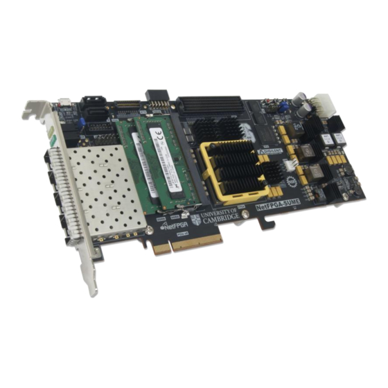
The NetFPGA-SUME board.
Expansion Connectors
QTH Connector (8 GTH transceivers)
One HPC FMC Connector (10 GTH transceivers
and 68 User I/Os)
One 12-pin Pmod port (8 User I/Os)
Programming
Micro USB Connector for JTAG programming and
debugging (shared with USB-UART interface)
Xilinx CPLD XC2C512 for FPGA configuration from
parallel flash
Power Management
Two Linear Technology Power System Managers
(LTC2974)
Provide current measuring on all major
power rails
Other Features
User LEDs and Push Buttons
PROG Push Button for manual FPGA Reset
FPGA Configuration LEDs
I2C Mux (PCA9548A) for controlling all onboard
I2C buses
1300 Henley Court
Pullman, WA 99163
509.334.6306
www.digilentinc.com
Page 1 of 18
Advertisement
Table of Contents

Subscribe to Our Youtube Channel
Related Manuals for Digilent NetFPGA-SUME


Summary of Contents for Digilent NetFPGA-SUME
- Page 1 1300 Henley Court Pullman, WA 99163 509.334.6306 www.digilentinc.com NetFPGA-SUME™ Reference Manual Revised April 11, 2016 This manual applies to the NetFPGA-SUME rev. C Overview Powered by Xilinx's Virtex-7 XC7V690T FPGA, the NetFPGA-SUME is an ideal platform for high-performance and high-density networking design.
- Page 2 ChipScope™ and EDK. The Virtex-7 XC7V690T FPGA is not a WebPack device, which means full licenses will need to be acquired for these tools in order to build designs that target the NetFPGA-SUME. Licensing information for Vivado can be found here. Academic institutes can make a request to the Xilinx University Program for a donation of full Vivado licenses here.
-
Page 3: Input Supply
Input Supply The NetFPGA-SUME receives power via a 2 x 4 pin PCI Express Auxiliary Power Connector. The 2x4 pin PCI Express Auxiliary Power receptacle (header J14) can accept both 2x3 and 2x4 pin PCI Express Auxiliary Power Plugs found on a standard ATX power supply. - Page 4 150 watts of power. While the board may be powered by either a 2x3 pin or a 2x4 pin PCI Express Auxiliary Power plug, due to the potential for high power consumption, Digilent recommends using a 2x4 pin plug to provide power whenever possible.
- Page 5 OUT4 clock. The use of out of phase clocks reduces the input RMS ripple current. Figure 5. LTC6909 clock output phase relationship. Copyright Digilent, Inc. All rights reserved. Page 5 of 18 Other product and company names mentioned may be trademarks of their respective owners.
- Page 6 Figure 6. Regulator topology. Power Sequencing and Supervising The components on the NetFPGA-SUME require that the supply voltages be sequenced on and off in a particular order. The NetFPGA-SUME utilizes two Linear Technology LTC2974s to ensure that these sequencing requirements are met.
- Page 7 2. VCC1V8 3. VCC2V0 4. MGTAVCC 5. MGTAVTT 6. VCC3V3 7. VCC1V5, QDRVTT, and DDRVTT 8. MGTVAUX Copyright Digilent, Inc. All rights reserved. Page 7 of 18 Other product and company names mentioned may be trademarks of their respective owners.
- Page 8 MGTVAUX 1.62V 1.665V 1.8V 1.935V 1.98V DDRVTT 0.75V QDRVTT 0.75V Table 2. Voltage fault and warning limits. Copyright Digilent, Inc. All rights reserved. Page 8 of 18 Other product and company names mentioned may be trademarks of their respective owners.
- Page 9 CLEAR_FAULTS command has been sent to both of the LTC2974s (IC43 and IC44). Figure 9. ALERTB interrupt source. Copyright Digilent, Inc. All rights reserved. Page 9 of 18 Other product and company names mentioned may be trademarks of their respective owners.
- Page 10 FAULTB1 pin. However, it has been pre-configured by Digilent during manufacturing to serve strictly as an output that indicates when any channel has faulted off. The FAULTB1 pin of the two LTC2974s are connected in a wire-and fashion to the gate of a transistor (N-FET). This transistor connects to the PCON_FAULT1 net, which is in turn connected to pin N40 of the FPGA, as shown in Fig.
-
Page 11: Power Consumption
NetFPGA-SUME™ Reference Manual Power Consumption The power consumed by the NetFPGA-SUME is largely dependent on the number of resources utilized by a given design, and the complexity of that design. This makes estimating power consumption for any particular application difficult. However, during the design process it was necessary to estimate the worst case scenario power consumption for each of the supply rails and to come up with a total power budget. -
Page 12: Fpga Configuration
After power-on, the Virtex-7 FPGA must be configured (or programmed) before it can perform any functions. You can configure the FPGA in one of two ways: A PC can use the Digilent USB-JTAG circuitry (port J16, labeled "PROG") to program the FPGA any time the power is on. ... -
Page 13: Jtag Configuration
FPGA over a 32-bit SelectMAP interface clocked at 100MHz. Digilent designed the firmware for the CPLD so that four different bitstreams can be stored in the flash. On power- up (if JP1 is not loaded), one of these bitstreams is read by the CPLD and used to program the FPGA. The bitstream that is used is determined by a non-volatile register called the "Boot Section Select"... -
Page 14: Ddr3 Sodimm
The QDRII+ SRAMs on NetFPGA-SUME board are capable of operating at up to 500MHz to yield data transfer rates of up to 1GT/s per 36-bit wide data bus. The Xilinx Memory Interface Generator (MIG) is able to generate and configure a native interface into the QDRII+ via the user friendly wizard tool. -
Page 15: Microsd Card
SATA The NetFPGA-SUME board provides two SATA ports which are SATA-III compatible (6Gbps). Two GTX transceivers (Lane 0,1 on Bank 116) are dedicated to these two ports with a master clock of 150MHz generated by Discera DSC1103 Low Jitter Precision LVDS Oscillator. SATA PHY controller can be generated using Xilinx GTX Transceiver Wizard. - Page 16 10Gb Ethernet ports, the output clock frequency of SI5324 is set to be 156.25MHz (Please refer to reference design in NetFPGA-SUME repository for recommended configuration values). The transceivers for both SATA connectors (Lane 0, 1 Bank 116) run from a 150MHz SATA_CLK (Bank 116 CLK0) generated by a low- jitter LVDS Oscillator (IC21 DSC1103).
-
Page 17: Expansion Interfaces
Pmod The NetFPGA-SUME board also provides a Pmod port for peripheral extension. The Pmod port is arranged as a 2×6 vertical, 100-mil female connector that mates with standard 2×6 pin headers. Each 12-pin Pmod port provides two Copyright Digilent, Inc. All rights reserved. - Page 18 Basic I/O The NetFPGA-SUME board includes two LEDs (LD0 and LD1) and two pushbuttons (BTN0 and BTN1) that can be used for basic user I/O. These can be useful for debugging designs. The pushbuttons are connected to the FPGA via series resistors to prevent damage from inadvertent short circuits (a short circuit could occur if an FPGA pin assigned to a pushbutton or slide switch was inadvertently defined as an output).
- Page 19 Mouser Electronics Authorized Distributor Click to View Pricing, Inventory, Delivery & Lifecycle Information: Digilent 410-301P-KIT 410-301...
Need help?
Do you have a question about the NetFPGA-SUME and is the answer not in the manual?
Questions and answers