Table of Contents
Advertisement
7/30/2019
Cora Z7 Reference Manual
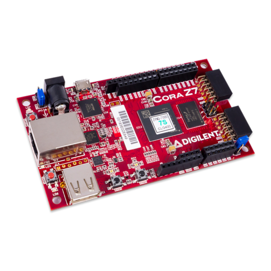
The Digilent Cora Z7 is a ready-to-use, low-cost, and easily embeddable development platform designed around the powerful Zynq-7000
All-Programmable System-on-Chip (APSoC) from Xilinx. The Zynq-7000 architecture tightly integrates a single or dual core 667MHz ARM
Cortex-A9 processor with a Xilinx 7-series FPGA. This pairing grants the ability to surround the processor with a unique set of software
defined peripherals and controllers, tailored for the target application.
The Cora Z7's wide array of hardware interfaces, from a 1Gbps Ethernet PHY to analog-to-digital converters and general-purpose
input/output pins, make it an ideal platform for the development of a vast variety of embedded applications. The small form factor and
mounting holes make the Cora Z7 ready to be used as one component of a larger solution. The on-board SD Card slot, Ethernet, and
Power solution allow the Cora Z7 to operate independently of a host computer.
(https://reference.digilentinc.com/_media/reference/programmable-logic/cora-z7/cora-obl-600.png)
https://reference.digilentinc.com/reference/programmable-logic/cora-z7/reference-manual?_ga=2.21685883.1349070004.1564406803-1961480359.1... 1/23
Cora Z7 Reference Manual [Reference.Digilentinc]
Advertisement
Table of Contents

Related Manuals for Digilent Cora Z7


Summary of Contents for Digilent Cora Z7
- Page 1 The small form factor and mounting holes make the Cora Z7 ready to be used as one component of a larger solution. The on-board SD Card slot, Ethernet, and Power solution allow the Cora Z7 to operate independently of a host computer.
- Page 2 7/30/2019 Cora Z7 Reference Manual [Reference.Digilentinc] https://reference.digilentinc.com/reference/programmable-logic/cora-z7/reference-manual?_ga=2.21685883.1349070004.1564406803-1961480359.1… 2/23...
- Page 3 7/30/2019 Cora Z7 Reference Manual [Reference.Digilentinc] Features ZYNQ Processor 667MHz dual-core (*single-core) Cortex-A9 processor FPGA Programmable logic equivalent to Artix-7 FPGA 4,400 Programmable logic slices (*3,600) 80 DSP slices (*60) 270 KB of block RAM () (*225 KB) DDR3 memory controller with 8 DMA channels and 4 High Performance AXI3 Slave ports High-bandwidth peripheral controllers: 1G Ethernet, USB 2.0, SDIO...
- Page 4 7/30/2019 Cora Z7 Reference Manual [Reference.Digilentinc] 512MB DDR3 with 16-bit bus @ 1050Mbps microSD slot Power Powered from USB or any 4.5V-5.5V external power source USB and Ethernet Gigabit Ethernet PHY with 48-bit globally unique EUI-48/64™ compatible identifier available on sticker...
-
Page 5: Software Support
Purchasing Options and Board Variants The Cora Z7 can be purchased with either a Zynq-7010 or Zynq-7007S loaded. These two Cora Z7 product variants are referred to as the Cora Z7-10 and Cora Z7-07S, respectively. When Digilent documentation describes functionality that is common to both of these variants, they are referred to collectively as the “Cora Z7”. -
Page 6: Functional Description
1 Power Supplies The Cora Z7 requires a 5 Volt power source to operate. This power source can come from the Digilent USB-JTAG port (J12) or it can be derived from a 5 Volt DC power supply connected to the Power Jack (J15). Unlike other Digilent FPGAs, the Cora Z7 cannot be powered through the Shield Header. -
Page 7: Zynq Apsoc Architecture
IC15: Dialog Semiconductor 100mA DA9062 Table 1.1. Cora Z7 Power Rails. With JP3 set to “USB” 2 Zynq APSoC Architecture The Zynq APSoC is divided into two distinct subsystems: The Processing System (PS) and the Programmable Logic (PL). Figure 2.1 shows an overview of the Zynq APSoC architecture, with the PS colored light green and the PL in yellow. - Page 8 Zynq Technical Reference Manual (http://www.xilinx.com/support/documentation/user_guides/ug585-Zynq-7000- TRM.pdf) Table 2.1 depicts the external components connected to the MIO pins of the Cora Z7. The Zynq Presets File found on the Cora Z7 Resource Center can be imported into EDK and Vivado Designs (https://reference.digilentinc.com/reference/programmable-logic/cora-z7/start) to properly configure the PS to work with these peripherals.
- Page 9 7/30/2019 Cora Z7 Reference Manual [Reference.Digilentinc] 1 (N/C) MODE0 MODE1 MODE2 MODE3 MODE4 VCFG0 VCFG1 Ethernet Reset Ethernet Interrupt USB Over Current Shield Reset 13 (N/C) UART Input UART Output MIO 501 (1.0V) Peripherals ETH 0 USB 0 SDIO 0...
-
Page 10: Zynq Configuration
7/30/2019 Cora Z7 Reference Manual [Reference.Digilentinc] DATA4 DATA0 DATA1 DATA2 DATA3 DATA5 DATA6 DATA7 CCLK RESETN 48 (N/C) 49 (N/C) 50 (N/C) 51 (N/C) MDIO Table 2.1. MIO Pinout 3 Zynq Configuration https://reference.digilentinc.com/reference/programmable-logic/cora-z7/reference-manual?_ga=2.21685883.1349070004.1564406803-1961480359.… 10/23... -
Page 11: Microsd Boot Mode
BootROM. If and only if the Zynq was just powered on, the BootROM will first latch the state of the mode pins into the mode register (the mode pins are attached to JP2 on the Cora Z7). If the BootROM is being executed due to a reset event, then the mode pins are not latched, and the previous state of the mode register is used. -
Page 12: Usb Uart Bridge (Serial Port)
533 MHz ()/1066 Mbps are supported. The Cora Z7 was routed with 40 ohm (+/-10%) trace impedance for single-ended signals, and differential clock and strobes set to 80 ohms (+/-10%). A feature called DCI (Digitally Controlled Impedance) is used to match the drive strength and termination impedance of the PS pins to the trace impedance. -
Page 13: Microsd Slot
The DTR signal from the UART controller on the FT2232HQ is connected to MIO12 of the Zynq device via JP1. Should the Arduino IDE be ported to work with the Cora Z7, this jumper can be shorted and MIO12 could be used to place the Cora Z7 in a “ready to receive a new sketch”... -
Page 14: Ethernet Phy
The Cora Z7 is technically an “embedded host”, because it does not provide the required 150 µF of capacitance on VBUS required to qualify as a general purpose host. It is possible to modify the Cora Z7 so that it complies with the general purpose USB host requirements by loading C35 with a 150 µF capacitor. -
Page 15: Clock Sources
9 Clock Sources The Cora Z7 provides a 50 MHz () clock to the Zynq PS_CLK input, which is used to generate the clocks for each of the Processing System (PS) subsystems. The 50 MHz () input allows the processor to operate at a maximum frequency of 650 MHz () and the DDR3 memory controller to operate at a maximum of 525 MHz () (1050 Mbps). - Page 16 The Zynq Processing System (PS) supports external power-on reset signals. The power-on reset is the master reset of the entire chip. This signal resets every register in the device capable of being reset. The Cora Z7 drives this signal from the nRESET signal of the DA9062 DC- DC converter system in order to hold the system in reset until all power supplies are valid.
-
Page 17: Tri-Color Leds
11.1 Tri-Color LEDs The Cora Z7 board contains two tri-color LEDs. Each tri-color LED () has three input signals that drive the cathodes of three smaller internal LEDs: one red, one blue, and one green. Driving the signal corresponding to one of these colors high will illuminate the internal LED (). - Page 18 0V-1.0V. Note: The Cora Z7 is not compatible with shields that output 5V digital or analog signals. Driving pins on the Cora Z7 shield connector above 5V may cause damage to the FPGA.
- Page 19 N / C IOREF Digital I/O Connected to the Cora Z7 3.3V Power Rail (See the “Power Supplies” section) Voltage reference Reset to Shield Connected to the red “SRST” button and a Digital I/O of the FPGA. When JP1 is shorted, it is also connected to the DTR signal of the FTDI USB-UART bridge.
- Page 20 The pins labeled A0-A11 and V_P/V_N are used as analog inputs to the XADC module of the FPGA. The FPGA expects that the inputs range from 0-1 V. On the pins labeled A0-A5, the Cora Z7 uses an external circuit to scale down the input voltage from 3.3V. This circuit is shown in Figure 13.2.1.
- Page 21 The Cora Z7 has an additional 12 Digital I/O pins in the form of a 16-pin unloaded expansion header (J1). The two outer-most pins (labeled V) of this header are connected to the Cora Z7's 3.3V rail. The next two outermost pins (labeled G) are connected to ground. The remaining 12 pins (labeled IO2-IO13) are directly connected to the Zynq PL.
- Page 22 Tree topology instead of fly-by was also among the routing recommendations for DDR3 layouts. So the Cora Z7 was designed with this sub-optimal layout due to space constraints. During Write Leveling calibration, 0 is used as an initial value instead of the negative preset delays.
- Page 23 7/30/2019 Cora Z7 Reference Manual [Reference.Digilentinc] (https://www.facebook.com/Digilent) (https://www.youtube.com/user/DigilentInc) (https://instagram.com/digilentinc) (https://github.com/digilent) (https://www.reddit.com/r/digilent) (https://www.linkedin.com/company/1454013) (https://www.flickr.com/photos/127815101@N07) https://reference.digilentinc.com/reference/programmable-logic/cora-z7/reference-manual?_ga=2.21685883.1349070004.1564406803-1961480359.… 23/23...
Need help?
Do you have a question about the Cora Z7 and is the answer not in the manual?
Questions and answers