Table of Contents
Advertisement
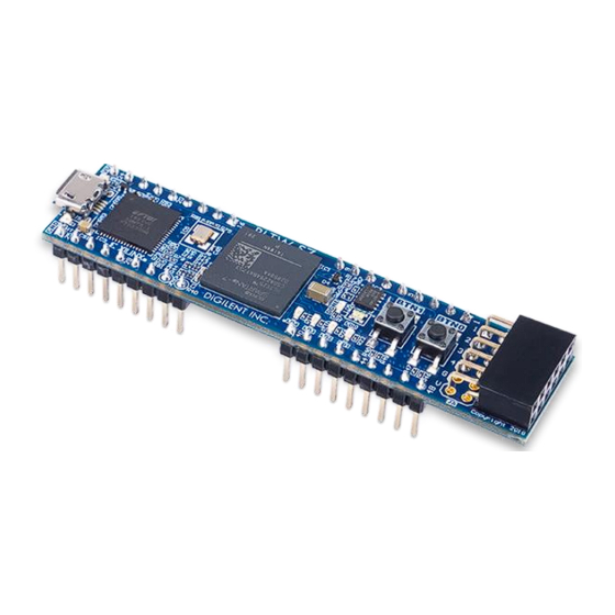
PLTW S7 Reference Manual
Revised July 11, 2018
This manual applies to the PLTW S7 rev. A
Overview
The PLTW S7 is a small, 48-pin DIP form factor board built around a Xilinx Spartan-7 FPGA. 32 FPGA digital I/O
signals, 2 FPGA analog input signals, an external power input rail, and a ground are routed to 100-mil-spaced
through-hole pins, making the PLTW S7 well-suited for use with solderless breadboards. At just 0.7" by 3.05"
inches, it can be loaded in a standard socket and used in embedded systems. The board includes a programming
ROM, clock source, USB programming and data transfer circuit, power supplies, LEDs, and buttons.
Features Include:
•
Xilinx Spartan-7 FPGA (XC7S25-1CSGA225C)
o
3,650 slices containing four 6-input
LUTs and 8 flip-flops
o
1,620 Kbits of fast block RAM
o
3 clock management tiles, each with
a phase-locked loop and mixed-
mode clock manager
o
80 DSP slices
o
Internal clock speeds exceeding
450 MHz
o
On-chip analog-to-digital converter
(XADC)
o
Programmable over JTAG and Quad-
SPI Flash
•
Memory
o
4 MB Quad-SPI Flash
•
Power
o
Powered from USB or 5V external
supply connected to DIP pin 24
DOC#: 6002-500-019
The PLTW S7.
Copyright Digilent, Inc. All rights reserved.
Other product and company names mentioned may be trademarks of their respective owners.
•
USB
o
USB-JTAG programming circuitry
o
USB-UART bridge
•
Push-buttons and LEDs
o
2 Buttons
o
4 LEDs
o
1 RGB LED
•
Expansion Connectors
o
1 Pmod connector
▪
8 total FPGA I/O
o
48-pin DIP form-factor headers
▪
32 total FPGA I/O
▪
2 single-ended 0-3.3V
analog inputs to XADC
▪
2 power pins
1300 Henley Court
Pullman, WA 99163
509.334.6306
www.store. digilent.com
Page 1 of 11
Advertisement
Table of Contents

Related Manuals for Digilent PLTW S7


Summary of Contents for Digilent PLTW S7
- Page 1 Overview The PLTW S7 is a small, 48-pin DIP form factor board built around a Xilinx Spartan-7 FPGA. 32 FPGA digital I/O signals, 2 FPGA analog input signals, an external power input rail, and a ground are routed to 100-mil-spaced through-hole pins, making the PLTW S7 well-suited for use with solderless breadboards.
-
Page 2: Software Support
This free installation includes the ability to create MicroBlaze™ soft-core processor designs. The PLTW S7 can be used with Vivado 2017.4, but WebPACK installations of this version of Vivado may not contain the device files for the Spartan-7 FPGA used on the PLTW S7. See this... - Page 3 Power Input Options It is possible to power the PLTW S7 from either USB or from an external power supply attached to pins 24 and 25 of the DIP headers, labeled “VU” and “GND”, respectively. The required characteristics of a power source attached to either of these two options is outlined in Table 1.1.1.
-
Page 4: Fpga Configuration
JTAG port. A Spartan-7 25T bitstream is typically 9,935,224 bits. The time it takes to program the PLTW S7 can be decreased by compressing the bitstream before programming, and then allowing the FPGA to decompress the bitstream itself during configuration. -
Page 5: Quad-Spi Flash
PLTW S7 Reference Manual Quad-SPI Configuration Since the FPGA's memory on the PLTW S7 is volatile, it relies on the Quad-SPI flash memory to store the configuration between power cycles. This configuration mode is called Master SPI. The blank FPGA takes the role of master and reads the configuration file out of the flash device upon power-up. - Page 6 Oscillators/Clocks The PLTW S7 includes a 12 MHz crystal oscillator connected to pin M9 (an MRCC input on bank 14). This clock is intended to be used as a general-purpose system clock. The clock can drive MMCMs to generate clocks of various frequencies and with known phase relationships that may be needed throughout a design.
- Page 7 Basic I/O The PLTW S7 includes one RGB LED, 4 individual LEDs, and 2 push buttons, as shown in Figure 6.1. The push buttons are connected to the FPGA via series resistors to prevent damage from inadvertent short circuits (a short circuit could occur if an FPGA pin assigned to a button was inadvertently defined as an output).
- Page 8 Figure 6.1. PLTW S7 Basic I/O. DIP Header The PLTW S7 has a 48-pin DIP form factor connector, implemented as four 9-pin headers for connecting to breadboards and custom fixtures. The pins have 100 mil spacing, and the entire module is 0.7 inches by 3.05 inches.
- Page 9 Figure 7.1. DIP Pin Diagram. VU (pin 24) can be used to power the PLTW S7 when it is not connected to a USB Host. When the device is connected to a USB host, VU is driven by the 5V rail of the USB connector and can be used to power devices external to the PLTW S7.
-
Page 10: Pmod Connector
The PLTW S7 has one “standard” type Pmod connector, and the FPGA pin connections for it are described in Table 8.1. Standard Pmod connectors are connected to the FPGA via 200 Ohm series resistors. The series resistors Copyright Digilent, Inc. - Page 11 Pin 3 Pin 4 Pin 7 Pin 8 Pin 9 Pin 10 Table 8.1. PLTW S7 Pmod Pinout. Copyright Digilent, Inc. All rights reserved. Page 11 of 11 Other product and company names mentioned may be trademarks of their respective owners.
Need help?
Do you have a question about the PLTW S7 and is the answer not in the manual?
Questions and answers