Table of Contents
Advertisement
Quick Links
D
i
g
i
l
e
n
t
D
2
-
D
i
g
i
l
e
n
t
D
2
R
e
f
e
r
e
n
c
e
M
R
e
f
e
r
e
n
c
e
M
Revision: September 18, 2003
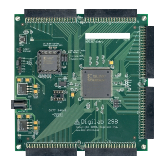
Overview
The Digilent D2-SB circuit board provides a
complete circuit development platform
centered on a Xilinx Spartan 2E FPGA. D2-SB
features include:
•
A Xilinx XC2S200E-200 FPGA with 200K
gates and 350MHz operation;
•
143 user I/Os routed to six standard 40-
pin expansion connectors;
•
A socket for a JTAG-programmable
18V02 configuration Flash ROM;
•
Dual on-board 1.5A power regulators
(1.8V and 3.3V);
•
An SMD 50MHz oscillator, and a socket
for a second oscillator;
•
A JTAG programming port;
•
A status LED and pushbutton for basic
I/O.
The D2-SB has been designed to work
seamlessly with all versions of the Xilinx ISE
CAD tools, including the free WebPack tools
available from the Xilinx website. A growing
collection of low-cost expansion boards can be
used with the D2-SB to add analog and digital
I/O capabilities, as well as various data ports
like Ethernet and USB. The D2-SB board ships
with a power supply and programming cable,
so designs can be implemented immediately
without the need for any additional hardware.
Functional Description
The Digilab D2-SB provides a minimal system
that can be used to rapidly implement FPGA-
based circuits, or to gain exposure to Xilinx
CAD tools and Spartan 2E devices. The D2-SB
provides only the essential supporting devices
for the Spartan 2E FPGA, including clock
sources and power supplies. All available I/O
signals are routed to standard expansion
connectors that mate with 40-pin, 100 mil
Copyright Digilent, Inc. All rights reserved
S
B
S
y
s
t
e
m
-
S
B
S
y
s
t
e
m
a
n
u
a
l
a
n
u
a
l
B
o
a
r
d
B
o
a
r
d
Power
1.8VDC
jack
regulator
5-9VDC
3.3VDC
regulator
Xilinx Spartan2E XC2S200E-PQ208
A1
D2-SB circuit board block diagram
spaced DIP headers available from any
catalog distributor. A pushbutton and LED are
also included for basic I/O.
The D2-SB board has been designed to serve
primarily as a host for peripheral boards. Each
of the six expansion connectors provides the
unregulated supply voltage (VU), 3.3V, GND,
and 32 FPGA I/O signals. Because there are
more connector pins than FPGA pins, the A1,
B1 and C1 connectors share an 18-pin "system
bus", and not all pins on the B expansion
connectors are used. JTAG signals are also
routed to the A1, B1, and C1 expansion
connectors. This allows peripheral boards to
drive the scan chain, or to be configured along
with the Spartan 2E FPGA.
Application-specific peripheral boards can be
created to mate with the D2-SB, or ready-
made peripheral boards that offer many
standard functions can be obtained from
Digilent (see www.digilentinc.com).
7 pages
www.digilentinc.com
246 East Main | Pullman, WA 99163
(509) 334 6306 Voice and Fax
ND
Clock
2
Push
Clock
button
(50MHz)
A2
B2
B1
C1
Config
LED
ROM
C2
Doc: 500-223
Advertisement
Table of Contents

Related Manuals for Digilent D2-SB


Summary of Contents for Digilent D2-SB
- Page 1 The D2-SB board has been designed to serve used with the D2-SB to add analog and digital primarily as a host for peripheral boards. Each I/O capabilities, as well as various data ports of the six expansion connectors provides the like Ethernet and USB.
- Page 2 FPGA and ROM on the TDI and TDO pins. In their default state, the D2-SB and then around the board to four Digilent port modules will appear as a JTAG connection ports as shown in the figure below.
- Page 3 3.3V on pin 3. Pins 4-35 route to FPGA I/O VCCO = 1.25(1 + R12/R11). signals, and pins 36-40 are reserved for JTAG Refer to the LM317 data sheet and D2-SB and/or clock signals. schematic for further information. The expansion headers provide 192 signal...
- Page 4 The “system bus” is a protocol used by certain The diagrams below show signal timings expansion boards that mimics a simple 8-bit assumed by Digilent to create peripheral microprocessor bus. It uses eight data lines, devices. However, any bus and timing models...
- Page 5 D2-SB Reference Manual Digilent, Inc. pins 4 -21 pins 22 -35 pins 4 -21 pins 22 -35 MB1(8) Spartan 2E Sys Bus (18) PQ 208 PB(18) pins 22 -35 pins 4 -21 pins 22 -35 pins 4 -21 Expansion Connector Signal Routing...
- Page 6 D2-SB Reference Manual Digilent, Inc. D2-SB Expansion Connector Pinout Pin # FPGA FPGA FPGA FPGA FPGA FPGA Signal Signal Signal Signal Signal Signal VCC33 VCC33 VCC33 VCC33 VCC33 VCC33 ADR0 112 PAI01 162 ADR0 112 PBI01 ADR0 112 PCI01 111 PAI02...
- Page 7 D2-SB Reference Manual Digilent, Inc. FPGA Pin Assignments Pin # Function Pin # Function Pin # Function Pin # Function VCCO VCCO PROG PC-IO17 PB-IO14 INIT PC-IO16 PB-IO13 ADR2 PA-IO3 PC-IO15 PB-IO12 PA-IO2 PC-IO14 PB-IO11 ADR1 PA-IO1 PC-IO13 PB-IO10 MA1-INT...
Need help?
Do you have a question about the D2-SB and is the answer not in the manual?
Questions and answers