Table of Contents
Advertisement
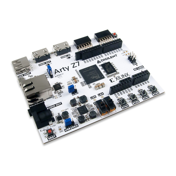
Arty Z7 Reference Manual
The Arty Z7 is a ready-to-use development platform designed around the Zynq-7000™ All
Programmable System-on-Chip (AP SoC) from Xilinx. The Zynq-7000 architecture tightly
integrates a dual-core, 650 MHz ARM Cortex-A9 processor with Xilinx 7-series Field
Programmable Gate Array (FPGA) logic. This pairing grants the ability to surround a
powerful processor with a unique set of software defined peripherals and controllers, tailored
by you for the target application.
The Vivado, Petalinux, and SDSoC toolsets each provide an approachable path between
defining your custom peripheral set and bringing it's functionality up to a Linux OS or bare
metal program running on the processor. For those looking for a more traditional digital logic
design experience, it is also possible to ignore the ARM processors and program the Zynq's
FPGA like you would any other Xilinx FPGA. Digilent provides a number of materials and
resources for the Arty Z7 that will get you up and running with your tool of choice quickly.
1
Arty Z7 Reference Manual
Transfer Multisort Elektronik / tme.eu
Advertisement
Table of Contents

Related Manuals for Digilent Arty Z7


Summary of Contents for Digilent Arty Z7
- Page 1 ARM processors and program the Zynq's FPGA like you would any other Xilinx FPGA. Digilent provides a number of materials and resources for the Arty Z7 that will get you up and running with your tool of choice quickly. Arty Z7 Reference Manual...
- Page 2 Arty Z7 Reference Manual Transfer Multisort Elektronik / tme.eu...
- Page 3 16 Total FPGA I/O Arduino/chipKIT Shield connector ▪ Up to 49 Total FPGA I/O (see table below) ▪ 6 Single-ended 0-3.3V Analog inputs to XADC ▪ 4 Differential 0-1.0V Analog inputs to XADC Arty Z7 Reference Manual Transfer Multisort Elektronik / tme.eu...
- Page 4 The board can be purchased stand-alone or with a voucher to unlock the Xilinx SDSoC toolset. The SDSoC voucher unlocks a 1 year license and can only be used with the Arty Z7. After the license expires, any version of SDSoC that was released during this 1 year period can continue to be used indefinitely.
-
Page 5: Software Support
Those familiar with the older Xilinx ISE/EDK toolsets from before Vivado was released can also choose to use the Arty Z7 in that toolset. Digilent does not have many materials to support this, but you can always ask for help on the Digilent Forum. - Page 6 15VDC might cause permanent damage. A suitable external power supply is included with the Arty Z7 accessory kit. Similar to using an external power supply, a battery can be used to power the Arty Z7 by attaching it to the shield connector and setting jumper JP5 to “REG”. The positive terminal of the battery must be connected to the pin labeled “VIN”...
- Page 7 FPGA fabric that each also contain addressable control registers. Furthermore, cores implemented in the PL can trigger interrupts to the processors (connections not shown in Fig. 3) and perform DMA accesses to DDR3 memory. Arty Z7 Reference Manual Transfer Multisort Elektronik / tme.eu...
- Page 8 For a complete and thorough description, refer to the Zynq Technical Reference manual. Table 2.1 depicts the external components connected to the MIO pins of the Arty Z7. The Zynq Presets File found on the Arty Z7 Resource Center can be imported into EDK and Vivado Designs to properly configure the PS to work with these peripherals.
- Page 9 Zynq Boot Image, which includes a First Stage Bootloader (FSBL), a bitstream for configuring the programmable logic (optional), and a user application. The boot process is broken into three stages: Arty Z7 Reference Manual Transfer Multisort Elektronik / tme.eu...
- Page 10 Stage 0 After the Arty Z7 is powered on or the Zynq is reset (in software or by pressing SRST), one of the processors (CPU0) begins executing an internal piece of read-only code called the BootROM. If and only if the Zynq was just powered on, the BootROM will first latch the state of the mode pins into the mode register (the mode pins are attached to JP4 on the Arty Z7).
- Page 11 The three boot modes are described in the following sections. 3.1 microSD Boot Mode The Arty Z7 supports booting from a microSD card inserted into connector J9. The following procedure will allow you to boot the Zynq from microSD with a standard Zynq Boot Image created with the Xilinx tools: 1.
-
Page 12: Quad Spi Flash
The Arty Z7 is configured to boot in Cascaded JTAG mode, which allows the PS to be accessed via the same JTAG port as the PL. It is also possible to boot the Arty Z7 in Independent JTAG mode by loading a jumper in JP2 and shorting it. This will cause the PS to not be accessible from the onboard JTAG circuitry, and only the PL will be visible in the scan chain. - Page 13 Zynq Technical Reference manual. ¹Maximum actual clock frequency is 525 MHz on the Arty Z7 due to PLL limitation. 6 USB UART Bridge (Serial Port) The Arty Z7 includes an FTDI FT2232HQ USB-UART bridge (attached to connector J14) that lets you use PC applications to communicate with the board using standard COM port commands (or the tty interface in Linux).
- Page 14 Zynq device via JP1. Should the Arduino IDE be ported to work with the Arty Z7, this jumper can be shorted and MIO12 could be used to place the Arty Z7 in a “ready to receive a new sketch” state. This would mimic the behavior of typical Arduino IDE boot-loaders.
-
Page 15: Usb Host
8 USB Host The Arty Z7 implements one of the two available PS USB OTG interfaces on the Zynq device. A Microchip USB3320 USB 2.0 Transceiver Chip with an 8-bit ULPI interface is used as the PHY. The PHY features a complete HS-USB Physical Front-End supporting speeds of up to 480Mbs. -
Page 16: Ethernet Phy
Arty Z7 accessory kit). 9 Ethernet PHY The Arty Z7 uses a Realtek RTL8211E-VL PHY to implement a 10/100/1000 Ethernet port for network connection. The PHY connects to MIO Bank 501 (1.8V) and interfaces to the Zynq-7000 APSoC via RGMII for data and MDIO for management. - Page 17 1.8V HSTL Class 1 drivers. For this I/O standard an external reference of 0.9V is provided in bank 501 (PS_MIO_VREF). Mapping out the correct pins and configuring the interface is handled by the Arty Z7 Zynq Presets file, available on the Arty Z7 Resource Center.
- Page 18 10 HDMI The Arty Z7 contains two unbuffered HDMI ports: one source port J11 (output), and one sink port J10 (input). Both ports use HDMI type-A receptacles with the data and clock signals terminated and connected directly to the Zynq PL.
-
Page 19: Clock Sources
Whenever a sink is ready and wishes to announce its presence, it connects the 5V0 supply pin to the HPD pin. On the Arty Z7, this is done by driving the Hot Plug Assert signal high. Note this should only be done after a DDC channel slave has been implemented in the Zynq PL and is ready to transmit display data. - Page 20 Figure 11.1 outlines the clocking scheme used on the Arty Z7. Note that the reference clock output from the Ethernet PHY is used as the 125 MHz reference clock to the PL, in order to cut the cost of including a dedicated oscillator for this purpose. Keep in mind that CLK125 will be disabled when the Ethernet PHY (IC1) is held in hardware reset by driving the PHYRSTB signal low.
- Page 21 USB and Ethernet port status. 12.1 Tri-Color LEDs The Arty Z7 board contains two tri-color LEDs. Each tri-color LED has three input signals that drive the cathodes of three smaller internal LEDs: one red, one blue, and one green. Driving the signal corresponding to one of these colors high will illuminate the internal LED.
- Page 22 The frequency response of SK Butterworth Low-Pass Filter is shown in Figure 13.2. The AC analysis of the circuit is done using NI Multisim 12.0. Figure 13.2. Audio Output Frequency Response. Arty Z7 Reference Manual Transfer Multisort Elektronik / tme.eu...
- Page 23 The Zynq PS supports external power-on reset signals. The power-on reset is the master reset of the entire chip. This signal resets every register in the device capable of being reset. The Arty Z7 Reference Manual Transfer Multisort Elektronik / tme.eu...
- Page 24 Arty Z7 drives this signal from the PGOOD signal of the TPS65400 power regulator in order to hold the system in reset until all power supplies are valid. 14.2 Program Push Button Switch A PROG push switch, labeled PROG, toggles Zynq PROG_B. This resets the PL and causes DONE to be de-asserted.
- Page 25 49 pins connected to the Zynq PL for general purpose Digital I/O on the Arty Z7-20 and 26 on the Arty Z7-10. Due to the flexibility of FPGAs, it is possible to use these pins for just about anything including digital read/write, SPI connections, UART connections, I2C connections, and PWM.
- Page 26 SPI Data in See Section titled “Shield Digital I/O” SPI Slave Select Single-Ended See Section titled “Shield Analog I/O” A0-A5 Analog Input Differential Analog See Section titled “Shield Analog I/O” A6-A11 Input Arty Z7 Reference Manual Transfer Multisort Elektronik / tme.eu...
- Page 27 IO26-IO41 and A (IO42) are not accessible on the Arty Z7-10. Also, AN0-AN5 cannot be used as Digital I/O on the Arty Z7-10. This is due to fewer number of I/O pins being available on the Zynq-7010 than on the Zynq-7020.
- Page 28 16.2.1. This circuit allows the XADC module to accurately measure any voltage between 0V and 3.3V (relative to the Arty Z7's GND) that is applied to any of these pins. If you wish to use the pins labeled A0-A5 as Digital inputs or outputs, they are also connected directly to the Zynq PL before the resistor divider circuit (also shown in Figure 16.2.1) on the Arty Z7-20.
- Page 29 Converter”. It is also possible to access the XADC core directly using the PS, via the “PS-XADC” interface. This interface is described in full in chapter 30 of the Zynq Technical Reference manual. Arty Z7 Reference Manual Transfer Multisort Elektronik / tme.eu...
Need help?
Do you have a question about the Arty Z7 and is the answer not in the manual?
Questions and answers