Table of Contents
Advertisement
Quick Links
Advertisement
Table of Contents

Related Manuals for Artesyn MVME5100


Summary of Contents for Artesyn MVME5100
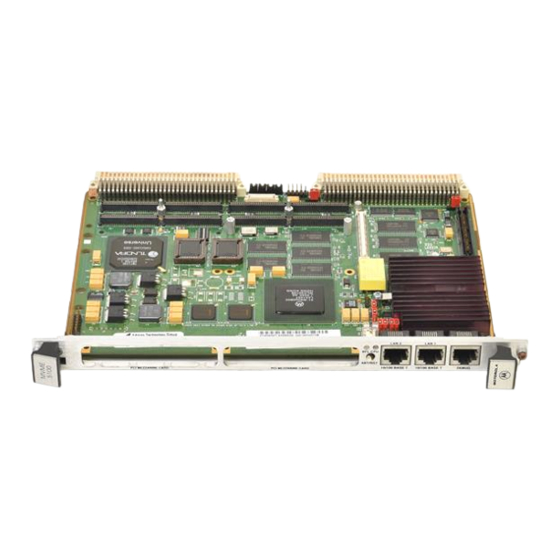
- Page 1 MVME5100 Single Board Computer Programmer’s Reference P/N: 6806800H17B July 2014...
- Page 2 Artesyn reserves the right to revise this document and to make changes from time to time in the content hereof without obligation of Artesyn to notify any person of such revision or changes.
-
Page 3: Table Of Contents
1.5.12 NVRAM/RTC & Watchdog Timer ..........51 MVME5100 Single Board Computer Programmer’s Reference (6806800H17B) - Page 4 2.4.9 Interprocessor Interrupts (IPI) ..........112 MVME5100 Single Board Computer Programmer’s Reference (6806800H17B)
- Page 5 Software Considerations ............269 MVME5100 Single Board Computer Programmer’s Reference (6806800H17B)
- Page 6 MVME5100 VPD Reference Information........
-
Page 7: Mvme5100 Single Board Computer Programmer's Reference (6806800H17B)
Related Documentation ............. . 313 Artesyn Embedded Technologies - Embedded Computing Documentation ....313 Manufacturer’s Documents . - Page 8 Contents Contents Contents MVME5100 Single Board Computer Programmer’s Reference (6806800H17B)
- Page 9 MVME5100 Status Register ........
- Page 10 PPC Slave Offset/Attribute (3) Registers ......... .147 MVME5100 Single Board Computer Programmer’s Reference (6806800H17B)
- Page 11 Timer Destination Registers ........... . 178 MVME5100 Single Board Computer Programmer’s Reference (6806800H17B)
- Page 12 Read/Write to ROM/Flash ............249 MVME5100 Single Board Computer Programmer’s Reference (6806800H17B)
- Page 13 Example of a Checksum Calculation: ..........307 Table B-1 MVME2700/MVME5100 Sample Slave Image Settings ......309 Table C-1 Artesyn Embedded Technologies - Embedded Computing Publications .
- Page 14 Related Specifications ............315 MVME5100 Single Board Computer Programmer’s Reference (6806800H17B)
- Page 15 MVME5100 Block Diagram ........
-
Page 16: List Of Figures
List of Figures MVME5100 Single Board Computer Programmer’s Reference (6806800H17B) -
Page 17: About This Manual
Appendix C, Related Documentation): PPCBug Firmware Package User’s Manual PPCBug Diagnostics Manual As of the printing date of this manual, the MVME5100 is available in the configurations shown below. Part Number Description 450 MHz MPC750 Commercial Models MVME5100-016x... - Page 18 PMCSPAN-002 with original VME Scan be ejector handles PMCSPAN1-010 PMCSAN-010 with original VME Scan be ejector handles RAM500-004 Stackable (top) 64MB ECC SDRAM mezzanine RAM500-006 Stackable (top) 256MB ECC SDRAM mezzanine RAM500-016 Stackable (bottom) 256MB ECC SDRAM mezzanine MVME5100 Single Board Computer Programmer’s Reference (6806800H17B)
- Page 19 Definitions. Appendix B, VMEbus Mapping Example, provides an example of a mapping scenario between an MVME5100 and an MVME2700 on a VMEbus backplane. Appendix C, Related Documentation, provides a listing of related Artesyn Embedded Technologies documents, vendor documentation and industry specifications.
- Page 20 MIDI Processing Unit/Peripheral Component Interconnect Memory Subsystem Data P2MX P2 multiplexing PCI/ISA PCIX Peripheral Component Interconnect Extended PFBR PCI Flush Before Read Hawk PCI Host Bridge PLCC/CLCC Plastic Leaded Chip Carrier/Ceramic Leadless Chip Carrier MVME5100 Single Board Computer Programmer’s Reference (6806800H17B)
- Page 21 Used to emphasize a word Used for on-screen output and code related elements Screen or commands in body text Used to characterize user input and to separate it Courier + Bold from system output MVME5100 Single Board Computer Programmer’s Reference (6806800H17B)
- Page 22 Indicates a hazardous situation which, if not avoided, may result in minor or moderate injury Indicates a property damage message No danger encountered. Pay attention to important information Terminology MVME5100 Single Board Computer Programmer’s Reference (6806800H17B)
- Page 23 16 bits, numbered 0 through 15, with bit 0 being the least significant. Word 32 bits, numbered 0 through 31, with bit 0 being the least significant. Double word 64 bits, numbered 0 through 63, with bit 0 being the least significant. MVME5100 Single Board Computer Programmer’s Reference (6806800H17B)
-
Page 24: Summary Of Changes
IPMC7xx ISA Bus Resources. Corrected incorrect address for DS1621 SROM. Added Appendix C, VMEbus Mapping Example. Added corrections/additions for CLK_FREQUENCY Register in Chapter 3. 6806800H17A 07/2009 Standardized contents. 6806800H17B July 2014 Re- branded to Artesyn template. MVME5100 Single Board Computer Programmer’s Reference (6806800H17B) -
Page 25: Product Data And Memory Maps
MPC7410 with AltiVec™ technology for algorithmic intensive computations or the low-power MPC750 or MPC755. The MVME5100 incorporates a highly optimized PCI interface and memory controller enabling up to 582MB/s memory read bandwidth and 640MB/s burst write bandwidth. The on-board Hawk ASIC provides the bridge function between the processor’s bus and the PCI bus. - Page 26 Two 32/64-bit PMC Slots with Front-Panel I/O Plus, P2 Rear I/O (MVME2300 Routing) One PCI Expansion Connector (for the PMCSpan) Miscellaneous Combined RESET and ABORT Switch Status LEDs Form Factor 6U VME MVME5100 Single Board Computer Programmer’s Reference (6806800H17B)
-
Page 27: Figure 1-1 Mvme5100 Block Diagram
Product Data and Memory Maps The following block diagram illustrates the architecture of the MVME5100 Single Board Computer. Figure 1-1 MVME5100 Block Diagram MVME5100 Single Board Computer Programmer’s Reference (6806800H17B) -
Page 28: Memory Maps
Following a reset, the memory map presented to the processor is identical to the CHRP memory map described in this document. The MVME5100 is fully capable of supporting both the PREP and the CHRP processor memory maps with ROM/FLASH size limited to 16MB and RAM size limited to 2GB. -
Page 29: Table 1-2 Default Processor Memory Map
For an example of the CHRP memory map refer to the following table. For detailed processor memory maps, including suggested CHRP- and Prep compatible memory maps, refer to the Hawk related portion of this manual. MVME5100 Single Board Computer Programmer’s Reference (6806800H17B) -
Page 30: Table 1-3 Suggested Chrp Memory Map
FLASH Bank A (preferred) 1, 2 FF80 0000 FF8F FFFF 1 MB FLASH Bank B (preferred) 1, 2 FF90 0000 FFEF FFFF 6 MB Reserved FFF0 0000 FFFF FFFF 1 MB Boot ROM MVME5100 Single Board Computer Programmer’s Reference (6806800H17B) -
Page 31: Table 1-4 Hawk Ppc Register Values For Suggested Memory Map
1.2.1.3 PCI Memory Map Following a reset, the Hawk ASIC disable’s all PCI slave map decoders. The MVME5100 is fully capable of supporting both PREP and CHRP PCI Memory Maps with RAM size limited to 2 GB. The default values for the PCI Slave Image registers, are listed in Chapter 3, PPCBug, of the MVME5100 Single Board Computer Installation and Use manual. -
Page 32: Pci Local Bus Memory Map
1.2.1.4 VME Memory Map The MVME5100 is fully capable of supporting both the PREP and the CHRP VME Memory Maps with RAM size limited to 2 GB. The default values for the VME Slave Image registers are listed in Chapter 3, PPCBug, of the MVME5100 Single Board Computer Installation and Use manual. -
Page 33: Processors
Serial Presence Detect (SPD) Definitions on page 36 1.3.1 Processors The MVME5100 has the BGA foot print that supports the MPC750, MPC755 and MPC7410 processors. The maximum external processor bus speed is 100 MHz. Parity checking is supported for the system address and data busses. 1.3.2 Processor Type Identification The processor version can be determined by reading the Processor Version Register (PVR). -
Page 34: Processor Pll Configuration
1.3.4 L2 Cache The MVME5100 SBC uses a back-door L2 cache structure via the Max processor chip. Max’s L2 cache is implemented with an onchip 2-way, set associative tag memory and external direct mapped synchronous SRAMs for data storage. The external SRAMs are accessed through a dedicated 72-bit wide (64-bits of data and 8 bits of address) L2 cache port on the processor. -
Page 35: Flash Memory
1.3.7 FLASH Memory The MVME5100 contains two banks of FLASH memory. Bank B consists of two 32-pin devices that can be populated with 1 MB of FLASH memory. Only 8-bit writes are supported for this bank. Bank A has 4 16-bit Smart Voltage FLASH SMT devices. With the 16 Mbit FLASH devices, the FLASH size is 8 MB. -
Page 36: P2 I/O Modes
MVME2400 models. The SBC mode is accomplished by configuring planar jumpers and attaching an IPMC761 PMC card in PMC slot 1 of the MVME5100. Refer to the IPMC712/761 I/O Module Installation and Use manual for additional installation and programming information. -
Page 37: Hawk I2C Interface And Configuration Information
Each slave device connected to the I2C bus is software addressable by a unique address. There can be seven slave devices connected to the I2C bus on the MVME5100. The VPD address is $A0. The UPD address is $A2. -
Page 38: Vital Product Data (Vpd) And Serial Presence Detect (Spd) Data
For information on the VPD and SPD data formats and definitions refer to Appendix A, MVME5100 VPD Reference Information. The registers related to this information is accessed through the I C interface of the Hawk ASIC. MVME5100 Single Board Computer Programmer’s Reference (6806800H17B) -
Page 39: Pci Local Bus
NVRAM/RTC & Watchdog Timer on page 51 Software Readable Header/Switch Register (S1) on page 52 Geographical Address Register (VME board) on page 53 Extended Features Register 1 on page 54 MVME5100 Single Board Computer Programmer’s Reference (6806800H17B) -
Page 40: Pci Arbitration Assignments For Hawk Asic
1.5.2 The Ethernet Controller The MVME5100 provides dual Ethernet interfaces (Port 1 and Port 2) via two pairs of Intel GD82559ER Fast Ethernet PCI controller chips. Port 1’s 10BaseT/100BaseTx interface is routed through the front panel. Port 2’s Ethernet interface is routed to either the front panel or the P2 connector, as configured by jumpers. -
Page 41: Pmc/Pci Expansion Slots
Up to two PMC slots and one PCIX slot may be present. The presence of the PMCs and/or PCIX can be positively determined by reading the Base Module Feature Register. The INTA#, INTB#, INTC#, and INTD# from the three PMC/PCIX slots are routed by the MVME5100 as follows: Figure 1-2 PMC/PCI Expansion Slots MVME5100 Single Board Computer Programmer’s Reference (6806800H17B) -
Page 42: The Universe Asic
Product Data and Memory Maps 1.5.4 The Universe ASIC The VMEbus interface is provided by the Universe ASIC. Figure 1-3 VMEbus Master Mapping MVME5100 Single Board Computer Programmer’s Reference (6806800H17B) -
Page 43: Pci Configuration Space
Access to PCI configuration space is accomplished via the Hawk ASIC using the CONADD and CONDAT Registers. The location and operation of these registers are fully described in Generating PCI Cycles on page 89. The IDSEL assignments for MVME5100 are shown on the following table: Table 1-7 IDSEL Mapping for PCI Devices... -
Page 44: Hawk External Register Bus Address Assignments
Hawk External Register Bus Address Assignments This section will describe in detail the Hawk External Register Bus Address Assignments on MVME5100. The address range for the External Register Set on MVME5100 is fixed at $FEF88000-$FEF8FFFF. MVME5100 Single Board Computer Programmer’s Reference (6806800H17B) -
Page 45: Table 1-9 Hawk External Register Bus Summary
Product Data and Memory Maps 1.5.6.1 MVME5100 Hawk External Register Bus Summary The Hawk External Register Summary of the MVME5100 is shown in the table below: Table 1-9 Hawk External Register Bus Summary Bits: REQUIRED (r) OPTIONAL (o) Address Register Name... -
Page 46: Dual Tl16C550 Uarts
UART - 2-SCR 1.5.7 Dual TL16C550 UARTs The MVME5100 implementation of the Dual TL16C550 UARTs are fully compliant with the PowerPlus II Programming Model for UART Registers. The following tables reflect this model. MVME5100 Single Board Computer Programmer’s Reference (6806800H17B) -
Page 47: Status Register
Product Data and Memory Maps The MVME5100 uses UART-1 and UART-2 for asynchronous serial debug ports (four are allowed by the PowerPlus II Programming Model). The first UART (UART-1) is addressed at External Register Set Address Offset $8000 (FEF8 8000). The second (UART-2) is addressed at offset $8200 (FEF8 8200). -
Page 48: Modfail Bit Register
This bit provides the current state of the FUSE signal. If set, at least one of the planar fuses or polyswitches is open. 1.5.9 MODFAIL Bit Register The MVME5100 implementation of this register is fully compliant with the PowerPlusII programming specification with exceptions to bit RD5, as indicated in the table. MVME5100 Single Board Computer Programmer’s Reference (6806800H17B) -
Page 49: Modrst Bit Register
ABORT_ signal is active. GREEN_LED This bit not used. 1.5.10 MODRST Bit Register The MODRST Bit register provides the means to reset the board. Table 1-13 MODRST Bit Register Module Reset Bit Register -FEF880A0h MVME5100 Single Board Computer Programmer’s Reference (6806800H17B) -
Page 50: Tben Bit Register
The host board is expected to assert a PCI reset when this signal is cleared. 1.5.11 TBEN Bit Register The MVME5100 implementation of this register is fully compliant with the PowerPlus II Programming Specification, with exceptions to Bit RD6, as indicated in the table. -
Page 51: Nvram/Rtc & Watchdog Timer
This bit is not used. 1.5.12 NVRAM/RTC & Watchdog Timer The MVME5100’s NVRAM/RTC and Watchdog Timer functions are supplied by an M48T37V device and is fully compliant with the PowerPlusII internal programming configuration. The M48T37V provides 32K of non-volatile SRAM, a time-of-day clock, and a watchdog timer. -
Page 52: Software Readable Header/Switch Register (S1)
Refer to the M48T37V Data Sheet for additional details and programming information. 1.5.13 Software Readable Header/Switch Register (S1) The MVME5100’s use of this register is fully compliant with the PowerPlus II internal programming configuration. A 1x8 header/switch (S1) is provided as the Software Readable Header/Switch (SRH). -
Page 53: Geographical Address Register (Vme Board)
5-row, 160-pin P1 connector. Table 1-17 Geographical Address Register (VME board) Geographical Address Register - Offset 80E8h FIELD GAP# GA4# GA3# GA2# GA1# GA0# OPER READ ONLY RESET REQUIRED REQUIRED ON MODULE WITH VME OPTIONAL MVME5100 Single Board Computer Programmer’s Reference (6806800H17B) -
Page 54: Extended Features Register 1
Memory Mezzanine 1 present. When set there is no memory mezzanine 1 present. When cleared, there is a memory mezzanine 1 present. MMEZ2_P_L Memory Mezzanine 2 present. When set, there is no memory mezzanine 1 present. When cleared, there is a memory mezzanine 2 present. MVME5100 Single Board Computer Programmer’s Reference (6806800H17B) -
Page 55: Board Last Reset Register
CompactPCI Reset. If set, a CompactPCI RST# reset has occurred. Not applicable for the MVME5100. CMDRST CompactPCI Command Reset. If set, a software reset command has been issued to the 21554 bridge from the CompactPCI bus. Not applicable for MVME5100. MVME5100 Single Board Computer Programmer’s Reference (6806800H17B) -
Page 56: Extended Features Register 2
The following subsections provide resource information pertaining to ISA bus resources that are present, if an IPMC712 or IPMC761 is mounted on the MVME5x00 Series Computer. They are accessible through the W83C554 PIB, which is present on the IPMC module. MVME5100 Single Board Computer Programmer’s Reference (6806800H17B) -
Page 57: W83C554 Pib Registers
Z85230 ESCC and Z8536 CIO Registers and Port Pins The Z85230 ESCC is used to provide the two sync/async serial ports on some MVME5100 series models. The PCLK which can be used to obtain the baud rates, is 10 MHz. Refer to the SCC User’s Manual for programming information on the Z85230 ESCC device. -
Page 58: Table 1-22 Z8536/Z85230 Access Registers
The assignment for the Port pins of the Z8536 CIO is as follows: Table 1-23 Z8536 CIO Port Pins Assignment Port Signal Name Direction Descriptions TM3_MID0 Input Port 3 Test Mode when IDREQ_ = 1; Module ID Bit 0 when IDREQ_ = 0. MVME5100 Single Board Computer Programmer’s Reference (6806800H17B) -
Page 59: Table
Port 4 Data Terminal Ready FUSE Input FUSE = 1 means that at least one of the fuses or polyswitches is open. ABORT_ Input Status of ABORT# signal Reserved Reserved Reserved Reserved Reserved Reserved Reserved MVME5100 Single Board Computer Programmer’s Reference (6806800H17B) -
Page 60: Table 1-24 Interpretation Of Mid3-Mid0
Module 4 Not Installed Because IDREQ_ and MID3-MID0 signals go through the P2MX (P2 multiplexing) function used on MVME5100 series boards configured for the MVME761-type transition module, software must wait for the MID3-MID0 to become valid after asserting IDREQ_. The waiting time should be about 4 microseconds because the sampling rate is about 1.6 microsecond... -
Page 61: Isa Dma Channels
Serial Port 4 Transmitter (Z85230 Port B Tx) Lowest Channel 7 Not Used Because the Z85230 is an 8-bit device and Channels 5 and 6 are 16-bit DMA Channels, only every other byte (the even bytes) from memory is valid. MVME5100 Single Board Computer Programmer’s Reference (6806800H17B) - Page 62 Product Data and Memory Maps MVME5100 Single Board Computer Programmer’s Reference (6806800H17B)
-
Page 63: Hawk Pci Host Bridge & Multi-Processor Interrupt Controller
Multi-level write post FIFO for writes to PCI Support for PPC bus clock speeds up to 100 MHz Selectable big or little endian operation 3.3 V signal levels MVME5100 Single Board Computer Programmer’s Reference (6806800H17B) - Page 64 Multilevel cross processor interrupt control for multiprocessor synchronization Four Interprocessor Interrupt sources Four 32-bit tick timers Processor initialization control Two 64-bit general For cross-processor messaging purpose registers MVME5100 Single Board Computer Programmer’s Reference (6806800H17B)
-
Page 65: Block Diagram
Hawk PCI Host Bridge & Multi-Processor Interrupt Controller Block Diagram Figure 2-1 Hawk PCI Host Bridge Block Diagram MVME5100 Single Board Computer Programmer’s Reference (6806800H17B) -
Page 66: Functional Description
During both write and read transactions, the PPC Slave places command information into the PPC FIFO. The PCI Master draws this command information from the PPC FIFO when it is ready to process the transaction. During write MVME5100 Single Board Computer Programmer’s Reference (6806800H17B) -
Page 67: Ppc Bus Interface
PPC Bus Interface The PPC Bus Interface connects directly to one MPC750 or MPC7400 microprocessor and one peripheral PPC60x master device. It uses a subset of the capabilities of the PPC bus protocol. MVME5100 Single Board Computer Programmer’s Reference (6806800H17B) -
Page 68: Figure 2-2 Ppc To Pci Address Decoding
There are no limits imposed by the PHB on how large of an address space a map decoder can represent. There is a lower limit of a minimum of 64 KB due to the resolution of the address compare logic. MVME5100 Single Board Computer Programmer’s Reference (6806800H17B) -
Page 69: Figure 2-3 Ppc To Pci Address Translation
PPC Slave will hold off asserting AACK_ and TA_ until after the transaction has completed on the PCI bus. This has the effect of removing all levels of pipelining MVME5100 Single Board Computer Programmer’s Reference (6806800H17B) -
Page 70: Table 2-2 Ppc Slave Response Command Types
ECOWX 10100 No Response TLB Invalidate 11000 Addr Only ECIWX 11100 No Response LWARX 00001 Addr Only STWCX 00101 Addr Only TLBSYNC 01001 Addr Only ICBI 01101 Addr Only Reserved 1XX01 No Response MVME5100 Single Board Computer Programmer’s Reference (6806800H17B) - Page 71 PPC transactions is delayed (AACK_ and TA_ are not asserted) until the PCI Master has completed a portion of the previously posted transactions and created some room within the command and/or data FIFOs. MVME5100 Single Board Computer Programmer’s Reference (6806800H17B)
-
Page 72: Table 2-3 Ppc Master Transaction Profiles And Starting Offsets
Discard read beat 0x00 Single @ 0x18 Burst @ 0x20 and 0x08 Burst @ 0x20 ..0x..18 -> 0x..1f Single @ 0x18 Single @ 0x18 Burst @ 0x20 Burst @ 0x20 ..MVME5100 Single Board Computer Programmer’s Reference (6806800H17B) -
Page 73: Table 2-4 Ppc Master Write Posting Options
If excessive latencies are encountered on the PPC60x bus, it may be necessary to tune the read ahead mechanism to compensate for this. Additional tuning of the read-ahead function is controlled by the RXFT/RMFT (Read Any FIFO Threshold/Read MVME5100 Single Board Computer Programmer’s Reference (6806800H17B) -
Page 74: Table 2-5 Ppc Master Read Ahead Options
PCI Slave map decoders. As an example, assume PHB has been programmed to respond to PCI address range $10000000 through $1001FFFF with an offset of $2000. The PPC Master performs its last read on the PPC60x bus at cache line address $3001FFFC or word address $3001FFF8. MVME5100 Single Board Computer Programmer’s Reference (6806800H17B) -
Page 75: Table 2-6 Ppc Master Transfer Types
PPC Master can be detrimental to the host CPU’s performance. The Bus Hog mode can be controlled by the XMBH bit within the GCSR. The default state for XMBH is disabled. MVME5100 Single Board Computer Programmer’s Reference (6806800H17B) -
Page 76: Table 2-7 Ppc Arbiter Pin Assignments
PHB has detected a rising edge on RST_. If the external arbiter mode has been selected, then XARB4 is driven to an active state no more than ten clock periods after PHB has detected a rising edge on RST_. MVME5100 Single Board Computer Programmer’s Reference (6806800H17B) - Page 77 If a data parity error is detected, then the PHB will latch address and attribute information within the ESTAT, EADDR, and EATTR registers, and an interrupt or machine check will be generated depending on the programming of the ESTAT register. MVME5100 Single Board Computer Programmer’s Reference (6806800H17B)
- Page 78 TA_ signals to close the pending data tenure. Error information related to the faulty transaction will be latched within the ESTAT, EADDR, and EATTR registers, and an interrupt or machine check will be generated depending on the programming of the ESTAT register. MVME5100 Single Board Computer Programmer’s Reference (6806800H17B)
-
Page 79: Pci Bus Interface
Configuration registers mapped into PCI Configuration space PPC bus address space mapped into PCI Memory space MPIC control registers mapped into either PCI I/O space or PCI Memory space Configuration Registers MVME5100 Single Board Computer Programmer’s Reference (6806800H17B) -
Page 80: Figure 2-4 Pci To Ppc Address Decoding
For each map, there is an independent set of attributes. These attributes are used to enable read accesses, enable write accesses, enable write posting, and define the PPC bus transfer characteristics. MVME5100 Single Board Computer Programmer’s Reference (6806800H17B) -
Page 81: Figure 2-5 Pci To Ppc Address Translation
When the PCI address falls into the range of more than one decoder, only the highest priority one will respond. The decoders are prioritized as shown below. Figure 2-6 PHB Address Decoder Priority MVME5100 Single Board Computer Programmer’s Reference (6806800H17B) -
Page 82: Table 2-8 Pci Slave Response Command Types
The following table shows which types of PCI cycles the slave has been designed to accept: Table 2-8 PCI Slave Response Command Types Command Type Slave Response? Interrupt Acknowledge Special Cycle I/O Read I/O Write MVME5100 Single Board Computer Programmer’s Reference (6806800H17B) - Page 83 The PCI Slave only honors the Linear Incrementing addressing mode. The PCI Slave performs a disconnect with data if any other mode of addressing is attempted. Device Selection The PCI slave will always respond valid decoded cycles as a medium responder. Target Initiated Termination MVME5100 Single Board Computer Programmer’s Reference (6806800H17B)
- Page 84 The PCI Slave does not have any hardware mechanisms in place to guarantee that the initial and subsequent target latency requirements are met. Typically this is not a problem since the bandwidth of the PPC bus far exceeds the bandwidth of the PCI bus. Exclusive Access MVME5100 Single Board Computer Programmer’s Reference (6806800H17B)
- Page 85 FIFO be the limiting factor. If either limit is exceeded then any pending PCI transactions are delayed (TRDY_ is not asserted) until the PPC Master has completed a portion of the previously posted transactions and created some room within the command and/or data FIFOs. MVME5100 Single Board Computer Programmer’s Reference (6806800H17B)
-
Page 86: Table 2-9 Pci Master Command Codes
Table 2-9 PCI Master Command Codes Entity Addressed TBST* C/BE PCI Command Transfer Type PIACK Read 0000 Interrupt Acknowledge CONADD/CONDAT Write 0001 Special Cycle Read 0010 I/O Read PPC Mapped PCI Space Write 0011 I/O Write MVME5100 Single Board Computer Programmer’s Reference (6806800H17B) - Page 87 PHB detected bridge lock. The same happens if the target responds with a disconnect and there is still data to be transferred. MVME5100 Single Board Computer Programmer’s Reference (6806800H17B)
- Page 88 The PCI Master is not able to initiate exclusive access transactions. Address/Data Stepping The PCI Master does not participate in the Address/Data Stepping protocol. Parity The PCI Master supports address parity generation, data parity generation, and data parity error detection. MVME5100 Single Board Computer Programmer’s Reference (6806800H17B)
- Page 89 The PHB performs contiguous I/O addressing when the MEM bit is clear and the IOM bit is clear. The PHB takes the PPC address, apply the offset specified in the XSOFFx register, and map the result directly to PCI. MVME5100 Single Board Computer Programmer’s Reference (6806800H17B)
-
Page 90: Figure 2-7 Pci Spread I/O Address Translation
The first step is to place the address of the configuration cycle within the CONFIG_ADDRESS register. Note that this action does not generate any cycles on the PCI bus. MVME5100 Single Board Computer Programmer’s Reference (6806800H17B) -
Page 91: Table 2-11 Device Number Decoding
The decoding of the five-bit Device Number is shown in the following table: Table 2-11 Device Number Decoding Device Number Address Bit 00000 AD31 00001 - 01010 All Zeros 01011 AD11 01100 AD12 (etc.) (etc.) MVME5100 Single Board Computer Programmer’s Reference (6806800H17B) - Page 92 PCI bus. Upon completion of the PCI interrupt acknowledge cycle, the PHB will present the resulting vector information obtained from the PCI bus as read data. MVME5100 Single Board Computer Programmer’s Reference (6806800H17B)
-
Page 93: Table 2-12 Pci Arbiter Pin Description
Once a lock cycle is detected, the grant is held asserted until the PCI LOCK_ pin is released. This feature works only when the “POL” bit is enabled. MVME5100 Single Board Computer Programmer’s Reference (6806800H17B) -
Page 94: Table 2-13 Fixed Mode Priority Level Setting
HAWK are defined in group 4. Arbitration is set for round robin mode between the 2 requestors within each group and set for fixed mode between the 4 groups. The levels of priority for each group are programmable by writing the “HEIR” field in the PCI Arbiter control register. MVME5100 Single Board Computer Programmer’s Reference (6806800H17B) -
Page 95: Table 2-14 Mixed Mode Priority Level Setting
All other combinations in the HEIR setting not specified in the table are invalid and should not be used. MVME5100 Single Board Computer Programmer’s Reference (6806800H17B) -
Page 96: Table 2-15 Arbitration Setting
When the “POL” bit in the PCI arbiter control register is set, the grant associated with the agent initiating the lock cycle will be held asserted until the lock cycle is complete. If this bit is clear, the arbiter does not distinguish between lock and non-lock cycle. MVME5100 Single Board Computer Programmer’s Reference (6806800H17B) -
Page 97: Endian Conversion
When all PPC devices are operating in big-endian mode, all data to/from the PCI bus must be swapped such that the PCI bus looks big endian from the PPC bus’s perspective. This association is true regardless of whether the transaction originates on the PCI bus or the PPC bus. MVME5100 Single Board Computer Programmer’s Reference (6806800H17B) -
Page 98: Figure 2-8 Big-To-Little-Endian Data Swap
When PPC Devices are Little Endian When all PPC devices are operating in little-endian mode, the originating address is modified to remove the exclusive-ORing applied by PPC60x processors. Note that no data swapping is performed. MVME5100 Single Board Computer Programmer’s Reference (6806800H17B) -
Page 99: Table 2-16 Address Modification For Little Endian Transfers
Big- Endian mode. This means that the processor’s internal view of the PPC registers appears different depending on which mode the processor operates. With respect to the PCI bus, the configuration registers are always represented in Little-Endian mode. MVME5100 Single Board Computer Programmer’s Reference (6806800H17B) -
Page 100: Error Handling
When any bit in the ESTAT is set, the PHB will attempt to latch as much information as possible about the error in the PPC Error Address (EADDR) and Attribute Registers (EATTR). MVME5100 Single Board Computer Programmer’s Reference (6806800H17B) -
Page 101: Watchdog Timers
PHB reset is asserted. External logic can use the output signals of the timers to generate interrupts, machine checks, etc. MVME5100 Single Board Computer Programmer’s Reference (6806800H17B) -
Page 102: Table 2-18 Wdtxcntl Programming
Byte Lane Selection Results ENAB RELOAD WDTxCNTL Register /RES Prescaler/ 8:15 16:23 24:31 Counter RES/ENAB RELOAD Enable No Change No Change No Change No Change Update Update No Change No Change from from RES/ENAB RELOAD MVME5100 Single Board Computer Programmer’s Reference (6806800H17B) - Page 103 FEFF0070 03FE0000 00000000 00000000 FFFFFFFF ....PPC1-Bug>mw feff0068 55;b Effective address: FEFF0068 Effective data : 55 PPC1-Bug>md feff0060 FEFF0060 000FFFFF 0000FFFF 004FFFFF 0000FFFF ..O... FEFF0070 03FE0000 00000000 00000000 FFFFFFFE ....PPC1-Bug>mw feff0068 aa0f5555 MVME5100 Single Board Computer Programmer’s Reference (6806800H17B)
-
Page 104: Pci/Ppc Contention Handling
Note that a mod-4 non-posted write transaction could be interrupted between write cycles, and thereby results in a partially completed write cycle. It is recommended that write cycles to write-sensitive, non-posted locations be performed on mod-4 address boundaries. MVME5100 Single Board Computer Programmer’s Reference (6806800H17B) - Page 105 There is a case where the processor could get starved for PCI read data while the PCI Slave is hosting multiple PPC60x bound write cycles. While attempting to perform a read from PCI space, the processor would continually get retried as a result of bridge lock resolution. MVME5100 Single Board Computer Programmer’s Reference (6806800H17B)
-
Page 106: Transaction Ordering
PHB PPC registers begins. The PCI Local Bus Specification 2.1 states that posted write buffers in both directions must be flushed before completing a read in either direction. MVME5100 Single Board Computer Programmer’s Reference (6806800H17B) - Page 107 PCI Slave can determine the transaction type. If it is a read and PFBR is enabled, the PCI Slave will look at the xs_fbrabt signal. If this signal is active, the PCI Slave will retry the PCI Master. MVME5100 Single Board Computer Programmer’s Reference (6806800H17B)
-
Page 108: Phb Hardware Configuration
PPC Register Base RD[5] Register Base = $FEFE0000 Parallel Interrupts MPIC Interrupt Type RD[7] Serial Interrupts Disabled PPC Arbiter Mode RD[8] Enabled Disabled PCI Arbiter Mode RD[9] Enabled PPC:PCI Clock Ratio RD[10:12] Reserved Reserved Reserved MVME5100 Single Board Computer Programmer’s Reference (6806800H17B) -
Page 109: Multi-Processor Interrupt Controller (Mpic)
Operation on page 121 Architectural Notes on page 123 Effects of Interrupt Serialization on page 123 2.4.1 MPIC Features The MPIC features are the following: MPIC programming model Supports two processors MVME5100 Single Board Computer Programmer’s Reference (6806800H17B) -
Page 110: Architecture
EINTT bit in the MPIC Global Configuration Register. If this bit is set, MPIC is in serial mode. Otherwise, MPIC operates in the parallel mode. In serial mode, all 16 external interrupts are serially scanned into MPIC using the SI_STA and SI_DAT pins as shown in the following figure. MVME5100 Single Board Computer Programmer’s Reference (6806800H17B) -
Page 111: Csr's Readability
In order for delivery of an interrupt to take place, the priority of the source must be greater than that of the destination processor. Therefore, setting a source priority to zero inhibits that interrupt. MVME5100 Single Board Computer Programmer’s Reference (6806800H17B) -
Page 112: Processor's Current Task Priority
IPI dispatch registers. If subsequent IPI’s are initiated before the first is acknowledged, only one IPI will be generated. The IPI channels deliver interrupts in Direct Mode and can be directed to more than one processor. MVME5100 Single Board Computer Programmer’s Reference (6806800H17B) -
Page 113: 8259 Compatibility
Each timer has four registers, which are used for configuration and control. They are the following: Current Count Register Base Count Register Vector-Priority Register Destination Register MVME5100 Single Board Computer Programmer’s Reference (6806800H17B) -
Page 114: Interrupt Delivery Modes
This is an arbitrary choice. 2.4.14 Block Diagram Description The description of the MPIC block diagram shown in the following figure focuses on the theory of operation for the interrupt delivery logic. MVME5100 Single Board Computer Programmer’s Reference (6806800H17B) - Page 115 The section discusses the following topics: Program Visible Registers on page 117 Interrupt Pending Register (IPR) on page 117 Interrupt Selector (IS) on page 117 Interrupt Request Register (IRR) on page 118 MVME5100 Single Board Computer Programmer’s Reference (6806800H17B)
-
Page 116: Figure 2-10 Mpic Block Diagram
Hawk PCI Host Bridge & Multi-Processor Interrupt Controller In-Service Register (ISR) on page 118 Interrupt Router on page 118 Figure 2-10 MPIC Block Diagram MVME5100 Single Board Computer Programmer’s Reference (6806800H17B) - Page 117 The IS also receives a second set of inputs from the ISR. During the End Of Interrupt cycle, these inputs are used to select which bits are to be cleared in the ISR. MVME5100 Single Board Computer Programmer’s Reference (6806800H17B)
- Page 118 Then one of these bits is delivered to each Interrupt Selector. Since this interrupt source can be multicast, each of these IPR bits must be cleared separately when the vector is returned for that interrupt to a particular processor. MVME5100 Single Board Computer Programmer’s Reference (6806800H17B)
-
Page 119: Programming Notes
TIE mode bit. This case is not defined in the above rule set. 2.4.15 Programming Notes This section discusses the following topics: External Interrupt Service on page 120 Reset State on page 121 MVME5100 Single Board Computer Programmer’s Reference (6806800H17B) - Page 120 If interrupts from ISA devices are directly connected to the MPIC (bypassing the 8259), the device driver interrupt service routine must read status from the ISA device to ensure buffers between the device and system memory are flushed. MVME5100 Single Board Computer Programmer’s Reference (6806800H17B)
-
Page 121: Operation
That is there is a total of four IPI dispatch registers in the MPIC. The IPI mechanism may be used for self interrupts by programming the dispatch register with the bit mask for the originating processor. MVME5100 Single Board Computer Programmer’s Reference (6806800H17B) - Page 122 8259 input on external interrupt source 0 directly through to processor zero. During interrupt controller initialization, this channel should be programmed for mixed mode in order to take advantage of the interrupt delivery modes. MVME5100 Single Board Computer Programmer’s Reference (6806800H17B)
-
Page 123: Architectural Notes
MPIC logic actually sees the change. Spurious interrupts can result if an EOI cycle occurs before the interrupt source is seen to be negated by MPIC logic. MVME5100 Single Board Computer Programmer’s Reference (6806800H17B) -
Page 124: Registers
The section discusses the following topics: on page 126 Revision ID Register on page 127 General Control-Status/Feature Registers on page 127 PPC Arbiter/PCI Arbiter Control Registers on page 130 MVME5100 Single Board Computer Programmer’s Reference (6806800H17B) -
Page 125: Table 2-20 Ppc Register Map For Phb
Table 2-20 PPC Register Map for PHB Bit---> $FEFF0000 VENID DEVID $FEFF0004 REVID $FEFF0008 GCSR $FEFF000C XARB PARB $FEFF0010 XPAD $FEFF0014 $FEFF0018 $FEFF001C $FEFF0020 ETEST EENAB $FEFF0024 ESTAT $FEFF0028 EADDR $FEFF002C EATTR $FEFF0030 PIACK MVME5100 Single Board Computer Programmer’s Reference (6806800H17B) -
Page 126: Table 2-21 Vendor Id/Device Id Registers
$FEFF006C WDT2STAT $FEFF0070 GPREG0(Upper) $FEFF0074 GPREG0(Lower) $FEFF0078 GPREG1(Upper) $FEFF007C GPREG1(Lower) Name VENID DEVID Operation Reset $1057 $4803 2.5.1.1 Table 2-21 Vendor ID/Device ID Registers Address $FEFF0000 Name VENID DEVID Operation Reset $1057 $4803 MVME5100 Single Board Computer Programmer’s Reference (6806800H17B) -
Page 127: Revision Id Register
Vendor ID. This register identifies the manufacturer of the device. This identifier is allocated by the PCI SIG to ensure uniqueness. $1057 has been assigned to Artesyn Embedded Technologies- Embedded Computing and is hardwired as a read-only value. This register is duplicated in the PCI Configuration Registers. - Page 128 PPC-initiated read transactions will be allowed to complete. When XFBR is clear, there is no correlation between these transaction types and their order of completion. Refer to the section titled Transaction Ordering for more information. XBTx MVME5100 Single Board Computer Programmer’s Reference (6806800H17B)
-
Page 129: Time-Out Length
PPC Arbiter. In a multiprocessor environment, these bits allow software to determine on which processor it is currently running. Table 2-25 PPC ID Time Out Length device on ABG0* device on ABG1* device on ABG2 Hawk MVME5100 Single Board Computer Programmer’s Reference (6806800H17B) -
Page 130: Ppc Arbiter/Pci Arbiter Control Registers
Flatten Single Write. This field is used by the PPC Arbiter to control how bus pipelining will be affected after all single beat write cycles. The encoding of this field is shown in the table below. Table 2-27 Flatten Single Write Field FBR/FSR/FBW/FSW Effects on Bus Pipelining None MVME5100 Single Board Computer Programmer’s Reference (6806800H17B) -
Page 131: Parking Field
The PCI Arbiter Register (PARB) provides control and status for the PCI Arbiter. Refer to Arbiter for more information. The bits within the PARB register are defined as follows: PRIx MVME5100 Single Board Computer Programmer’s Reference (6806800H17B) -
Page 132: Priority Field
0011 Park always on PARB4 0100 Park always on PARB3 0101 Park always on PARB2 0110 Park always on PARB1 0111 Park always on PARB0 1000 Park always on HAWK 1111 None HIERx MVME5100 Single Board Computer Programmer’s Reference (6806800H17B) -
Page 133: Table
Group 4 -> Group 1 -> Group 2 -» Group 3 Group 3 -> Group 4 -> Group 1 -> Group 2 Group 2 -> Group 3 -> Group 4 -> Group 1 Reserved Reserved Reserved Reserved MVME5100 Single Board Computer Programmer’s Reference (6806800H17B) -
Page 134: Table 2-33 Hardware Control-Status/Prescaler Adjust Register
XPAD Operation Reset XPRx PPC/PCI Clock Ratio. This is a read only field that is used to indicate the clock ratio that has been established by the PHB at the release of reset. MVME5100 Single Board Computer Programmer’s Reference (6806800H17B) -
Page 135: Ppc/Pci Clock Ratio Field
The encoding of this field is shown in the following table. Table 2-35 Write Lock Resolution Threshold WLRT Write lock resolution threshold Match write threshold mode (i.e. PSATTx WXFT) Immediate FIFO full FIFO full MVME5100 Single Board Computer Programmer’s Reference (6806800H17B) -
Page 136: Read Lock Resolution Threshold
Clk is the frequency of the CLK input in MHz. The following table shows the scale factors for some common CLK frequencies: Table 2-37 Common Scale Factors for Common CLK Frequencies Frequency XPAD MVME5100 Single Board Computer Programmer’s Reference (6806800H17B) -
Page 137: Ppc Error Test/Error Enable Register
In particular, each error type can uniquely be programmed to generate a machine check, generate an interrupt, generate both, or generate neither. The bits within the ETEST are defined as follows: DFLT MVME5100 Single Board Computer Programmer’s Reference (6806800H17B) - Page 138 PRTAM PCI Master Received Target Abort Machine Check Enable. When this bit is set, the PRTA bit in the ESTAT register will be used to assert the MCHK output to the bus master which initiated the transaction. When this bit is clear, MCHK will not be asserted. XBTOI MVME5100 Single Board Computer Programmer’s Reference (6806800H17B)
- Page 139 2.5.1.7 PPC Error Status Register The Error Status Register (ESTAT) provides an array of status bits pertaining to the various errors that the PHB can detect. MVME5100 Single Board Computer Programmer’s Reference (6806800H17B)
-
Page 140: Table 2-39 Ppc Error Status Register
MCHK to the master designated by the DFLT bit in the EATTR register. When the PPERI bit in the EENAB register is set, the assertion of this bit will assert an interrupt through the MPIC. MVME5100 Single Board Computer Programmer’s Reference (6806800H17B) -
Page 141: Ppc Error Address Register
The register’s contents are not defined when the XDPE, PPER or PSER bits are set in the ESTAT register. Table 2-40 PPC Error Address Register Address $FEFF0028 Name EAADR Operation Reset $00000000 MVME5100 Single Board Computer Programmer’s Reference (6806800H17B) -
Page 142: Ppc Error Attribute Register
Transfer Size. This field contains the transfer size of the PPC transfer in which the error occurred. Transfer Type. This field contains the transfer type of the PPC transfer in which the error occurred. MVME5100 Single Board Computer Programmer’s Reference (6806800H17B) -
Page 143: Ppc Error Attribute Register, Psma Or Prta Set
PCI Command. This field contains the PCI command of the PCI transfer in which the error occurred. BYTEx PCI Byte Enable. This field contains the PCI byte enables of the PCI transfer in which the error occurred. A set bit designates a selected byte. MVME5100 Single Board Computer Programmer’s Reference (6806800H17B) -
Page 144: Pci Interrupt Acknowledge Register
Start Address. This field determines the start address of a particular memory area on the PPC bus which will be used to access PCI bus resources. The value of this field will be compared with the upper 16 bits of the incoming PPC address. MVME5100 Single Board Computer Programmer’s Reference (6806800H17B) -
Page 145: Ppc Slave Offset/Attribute (0, 1 And 2) Registers
PPC memory space to PCI memory I/O space. The bits within the XSATTx registers are defined as follows: Read Enable. If set, the corresponding PPC Slave is enabled for read transactions. MVME5100 Single Board Computer Programmer’s Reference (6806800H17B) -
Page 146: Ppc Slave Address (3) Register
CONFIG_ADDRESS ($80000CF8) and CONFIG_DATA ($80000CFC) registers. The power up value of XSADD3 (and XSOFF3/XSATT3) are set to allow access to these special register spaces without PPC register initialization. The fields within XSADD3 are defined as follows: MVME5100 Single Board Computer Programmer’s Reference (6806800H17B) -
Page 147: Ppc Slave Offset/Attribute (3) Registers
PPC bus. It is initialized to $8000 to facilitate a zero based access to PCI space. The PPC Slave Attributes Register 3 (XSATT3) contains attribute information associated with the mapping of PPC memory space to PCI I/O space. The bits within the XSATT3 register are defined as follows: MVME5100 Single Board Computer Programmer’s Reference (6806800H17B) -
Page 148: Wdtxcntl Registers
WDTxCNTL registers are defined as follows: Key. This field is used during the two step arming process of the Control register. This field is sensitive to the following data patterns: PATTERN_1 = $55 MVME5100 Single Board Computer Programmer’s Reference (6806800H17B) -
Page 149: Res Field Options
8 us 512 msec 0100 16 us 1 sec 0101 32 us 2 sec 0110 64 us 4 sec 0111 128 us 8 sec 1000 256 us 16 sec 1001 512 us 32 sec MVME5100 Single Board Computer Programmer’s Reference (6806800H17B) - Page 150 Effective address: FEFF0068 Effective data : AA88 PPC6-Bug>md feff006c FEFF006C 0000B26D 03FE4000 00000000 00000000 ...m..@..FEFF007C FFFFFFFE FFFFFFFF FFFFFFFF FFFFFFFF ....PPC6-Bug>md feff006c FEFF006C 00006145 03FE4000 00000000 00000000 ..aE..@..FEFF007C FFFFFFFE FFFFFFFF FFFFFFFF FFFFFFFF ....MVME5100 Single Board Computer Programmer’s Reference (6806800H17B)
-
Page 151: Wdtxstat Registers
The Watchdog Timer Status Registers (WDT1STAT and WDT2STAT) are used to provide status information from the watchdog timer functions within the PHB. The field within WDTxSTAT registers is defined as follows: COUNT Count. This read-only field reflects the instantaneous counter value of the WDT. MVME5100 Single Board Computer Programmer’s Reference (6806800H17B) -
Page 152: Pci Registers
The PCI Configuration Register map of the PHB is shown in Table 2-52. The PCI I/O Register map of the PHB is shown in Table 2-53. Table 2-52 PCI Configuration Register <--Bit DEVID VENID STATUS COMMAND CLASS REVID HEADER MIBAR MVME5100 Single Board Computer Programmer’s Reference (6806800H17B) -
Page 153: Table
PCI Slave Address (0,1,2, and 3) Registers on page 160 PCI Slave Attribute/ Offset (0,1,2 and 3) Registers on page 161 CONFIG_ADDRESS Register on page 163 CONFIG_DATA Register on page 165 MVME5100 Single Board Computer Programmer’s Reference (6806800H17B) -
Page 154: Vendor Id/ Device Id Registers
Vendor ID. This register identifies the manufacturer of the device. This identifier is allocated by the PCI SIG to ensure uniqueness. $1057 has been assigned to Artesyn Embedded Technologies - Embedded Computing. This register is duplicated in the PPC Registers. - Page 155 PHB asserted PERR_ itself or observed PERR_ asserted the PHB was the PCI Master for the transfer in which the error occurred the PERR bit in the PCI Command Register is set MVME5100 Single Board Computer Programmer’s Reference (6806800H17B)
-
Page 156: Revision Id/ Class Code Registers
(see bit PERR in the PCI Command Register). It is cleared by writing it to 1; writing a 0 has no effect. 2.5.2.3 Revision ID/ Class Code Registers Table 2-56 Revision ID/ Class Code Registers Offset Name CLASS REVID MVME5100 Single Board Computer Programmer’s Reference (6806800H17B) -
Page 157: Header Type Register
Not Used 2.5.2.4 Header Type Register Table 2-57 Header Type Register Offset Name HEADER Operation Reset The Header Type Register (Header) identifies the PHB as follows: Header Type: $00 - Single Function Configuration Header MVME5100 Single Board Computer Programmer’s Reference (6806800H17B) -
Page 158: Mpic I/O Base Address Register
Base Address. These bits define the I/O space base address of the MPIC control registers. The MIBAR decoder is disabled when the BASE value is zero. 2.5.2.6 MPIC Memory Base Address Register Table 2-59 MPIC Memory Base Address Register Offset Name MMBAR MVME5100 Single Board Computer Programmer’s Reference (6806800H17B) - Page 159 Prefetch. This bit is hard-wired to zero to indicate that the MPIC registers are not prefetchable. BASE Base Address. These bits define the memory space base address of the MPIC control registers. The MBASE decoder is disabled when the BASE value is zero. MVME5100 Single Board Computer Programmer’s Reference (6806800H17B)
-
Page 160: Pci Slave Address (0,1,2, And 3) Registers
End Address. This field determines the end address of a particular memory area on the PCI bus which will be used to access PPC bus resources. The value of this field will be compared with the upper 16 bits of the incoming PCI address. MVME5100 Single Board Computer Programmer’s Reference (6806800H17B) -
Page 161: Pci Slave Attribute/ Offset (0,1,2 And 3) Registers
Read Ahead Enable. If set, read ahead is enabled for the corresponding PCI Slave. WPEN Write Post Enable. If set, write posting is enabled for the corresponding PCI Slave. Write Enable. If set, the corresponding PCI Slave is enabled for write transactions. MVME5100 Single Board Computer Programmer’s Reference (6806800H17B) -
Page 162: Rmftx Field
This field is only applicable if read-ahead has been enabled. The encoding of this field is shown in the table above: Table 2-63 WXFTx Field WXFT Write FIFO Threshold 4 Cache lines 3 Cache lines 2 Cache lines 1 Cache lines MVME5100 Single Board Computer Programmer’s Reference (6806800H17B) -
Page 163: Table 2-64 Conceptual Perspective From The Pci Bus
Table 2-64 Conceptual perspective from the PCI bus Offset $CFB $CFA $CF9 $CF8 Name CONFIG_ADDRESS Operation Reset Table 2-65 Perspective from the PPC bus in Big Endian mode Offset $CF8 $CF9 $CFA $CFB Bit (DH) Name CONFIG_ADDRESS Operation MVME5100 Single Board Computer Programmer’s Reference (6806800H17B) -
Page 164: Table 2-66 Perspective From The Ppc Bus In Little Endian Mode
Device Number. Configuration Cycles: Identifies a target’s physical PCI device number. Refer to the section on Generating PCI Cycles for a description of how this field is encoded. Special Cycles: This field must be written with all ones. MVME5100 Single Board Computer Programmer’s Reference (6806800H17B) -
Page 165: Table 2-67 Conceptual Perspective From The Pci Bus
Operation Reset Table 2-68 Perspective from the PPC bus in Big Endian mode Offset $CFC $CFD $CFE $CFF Bit (DH) Name CONFIG_DATA Data ‘A’ ’ Data ‘B’ Data ‘C’ Data ‘D’ Operation Reset MVME5100 Single Board Computer Programmer’s Reference (6806800H17B) -
Page 166: Mpic Registers
Timer Current Count Registers on page 175 Timer Basecount Registers on page 176 Timer Vector/Priority Registers on page 177 Timer Destination Registers on page 178 External Source Vector/Priority Registers on page 178 MVME5100 Single Board Computer Programmer’s Reference (6806800H17B) -
Page 167: Mpic Register Map
IPI3 VECTOR-PRIORITY REGISTER $010d0 SP REGISTER $010e0 TIMER FREQUENCY REPORTING REGISTER $010f0 TIMER 0 CURRENT COUNT REGISTER $01100 TIMER 0 BASE COUNT REGISTER $01110 TIMER 0 VECTOR-PRIORITY REGISTER $01120 TIMER 0 DESTINATION REGISTER $01130 MVME5100 Single Board Computer Programmer’s Reference (6806800H17B) - Page 168 INT. SRC. 10 DESTINATION REGISTER $10150 INT. SRC. 11 VECTOR-PRIORITY REGISTER $10160 INT. SRC. 11 DESTINATION REGISTER $10170 INT. SRC. 12 VECTOR-PRIORITY REGISTER $10180 INT. SRC. 12 DESTINATION REGISTER $10190 INT. SRC. 13 VECTOR-PRIORITY REGISTER $101a0 MVME5100 Single Board Computer Programmer’s Reference (6806800H17B)
-
Page 169: Feature Reporting Register
IPI 3 DISPATCH REGISTER PROC. 1 $21070 CURRENT TASK PRIORITY REGISTER PROC. 1 $21080 IACK REGISTER $210a0 EOI REGISTER $210b0 2.5.3.2 Feature Reporting Register Table 2-71 Feature Reporting Register Offset $01000 Name FEATURE REPORTING MVME5100 Single Board Computer Programmer’s Reference (6806800H17B) -
Page 170: Global Configuration Register
Version level of 02 is used for the initial release of the MPIC specification. 2.5.3.3 Global Configuration Register Table 2-72 Global Configuration Register Offset $01020 Name GLOBAL CONFIGURATION Operation Reset RESET MVME5100 Single Board Computer Programmer’s Reference (6806800H17B) -
Page 171: Cascade Mode Encoding
Processor 0 after a reset. When this register bit is set to 0, a tie in external interrupt processing will always go to processor 0 (Mode used on Version $02 of MPIC). Table 2-74 Tie Mode Encoding Mode Processor 0 always selected Swap between Processor’s MVME5100 Single Board Computer Programmer’s Reference (6806800H17B) -
Page 172: Vendor Identification Register
Offset $01090 Name PROCESSOR INIT Operation Reset PROCESSOR 1. Writing a 1 to P1 will assert the Soft Reset input of processor 1. Writing a 0 to it will negate the SRESET signal. MVME5100 Single Board Computer Programmer’s Reference (6806800H17B) -
Page 173: Ipi Vector/Priority Registers
The ACT bit is set to a one when its associated bit in the Interrupt Pending Register or In-Service Register is set. PRIOR PRIORITY. Interrupt priority 0 is the lowest and 15 is the highest. Note that a priority level of 0 will not enable interrupts. VECTOR MVME5100 Single Board Computer Programmer’s Reference (6806800H17B) -
Page 174: Spurious Vector Register
Following reset, this register contains zero. The system initialization code must initialize this register to one-eighth the MPIC clock frequency. For the PHB implementation of the MPIC, a typical value would be $7de290 (which is 66/8 MHz or 8.25 MHz). MVME5100 Single Board Computer Programmer’s Reference (6806800H17B) -
Page 175: Timer Current Count Registers
CURRENT COUNT. The current count field decrements while the Count Inhibit bit is the Base Count Register is zero. When the timer counts down to zero, the Current Count register is reloaded from the Base Count register and the timer’s interrupt becomes pending in MPIC processing. MVME5100 Single Board Computer Programmer’s Reference (6806800H17B) -
Page 176: Timer Basecount Registers
Count register and the toggle bit in the Current Count register is cleared. When the timer counts down to zero, the Current Count register is reloaded from the Base Count register and the timer’s interrupt becomes pending in MPIC processing. MVME5100 Single Board Computer Programmer’s Reference (6806800H17B) -
Page 177: Timer Vector/Priority Registers
PRIORITY. Interrupt priority 0 is the lowest and 15 is the highest. Note that a priority level of 0 will not enable interrupts. VECTOR VECTOR. This vector is returned when the Interrupt Acknowledge register is examined upon acknowledgment of the interrupt associated with this vector. MVME5100 Single Board Computer Programmer’s Reference (6806800H17B) -
Page 178: Timer Destination Registers
PROCESSOR 0. The interrupt is directed to processor 0. 2.5.3.13 External Source Vector/Priority Registers Table 2-84 External Source Vector/Priority Registers Int Src 0 - $10000 Offset Int Src 1-> Int Src15 - $10020 -> $101E0 Name EXTERNAL SOURCE VECTOR/PRIORITY PRIOR VECTOR MVME5100 Single Board Computer Programmer’s Reference (6806800H17B) - Page 179 Setting this bit to one enables active low level triggered interrupts. PRIOR PRIORITY. Interrupt priority 0 is the lowest and 15 is the highest. Note that a priority level of 0 will not enable interrupts. VECTOR MVME5100 Single Board Computer Programmer’s Reference (6806800H17B)
-
Page 180: External Source Destination Registers
PROCESSOR 0. The interrupt is pointed to processor 0. 2.5.3.15 Hawk Internal Error Interrupt Vector/Priority Register Table 2-86 Hawk Internal Error Interrupt Vector/Priority Register Offset $10200 Name HAWK INTERNAL ERROR INTERRUPT VECTOR/PRIORITY PRIOR VECTOR MVME5100 Single Board Computer Programmer’s Reference (6806800H17B) - Page 181 PRIORITY. Interrupt priority 0 is the lowest and 15 is the highest. Note that a priority level of 0 will not enable interrupts. VECTOR VECTOR. This vector is returned when the Interrupt Acknowledge register is examined upon acknowledgment of the interrupt associated with this vector. MVME5100 Single Board Computer Programmer’s Reference (6806800H17B)
-
Page 182: Hawk Internal Error Interrupt Destination Register
PROCESSOR 0. The interrupt is pointed to processor 0. 2.5.3.17 Interprocessor Interrupt Dispatch Registers Table 2-88 Interprocessor Interrupt Dispatch Registers Processor 0 $20040, $20050, $20060, $20070 Offset Processor 1 $21040, $21050,$21060, $21070 Name IPI DISPATCH Operation Reset MVME5100 Single Board Computer Programmer’s Reference (6806800H17B) -
Page 183: Current Task Priority Registers
Setting the Task Priority Register to 15 masks all interrupts to this processor. Hardware will set the task register to $F when it is reset or when the Init bit associated with this processor is written to a one. Task Priority of processor. MVME5100 Single Board Computer Programmer’s Reference (6806800H17B) -
Page 184: Interrupt Acknowledge Registers
Reading this register will update the In-Service register. VECTOR Vector. This vector is returned when the Interrupt Acknowledge register is read. 2.5.3.20 End-of-Interrupt Registers Table 2-91 End-of-Interrupt Registers Processor 0 $200B0 Offset Processor 1 $210B0 Name Operation Reset MVME5100 Single Board Computer Programmer’s Reference (6806800H17B) - Page 185 The write operation will update the In-Service register by retiring the highest priority interrupt. Reading this register returns zeros. MVME5100 Single Board Computer Programmer’s Reference (6806800H17B)
- Page 186 Hawk PCI Host Bridge & Multi-Processor Interrupt Controller MVME5100 Single Board Computer Programmer’s Reference (6806800H17B)
-
Page 187: System Memory Controller (Smc)
Two blocks with up to 256MB each at 100 MHz – Eight blocks with up to 256MB each at 66.67 MHz – Uses -8, -10, or PC100 SDRAMs – Programmable base address for each block – Built-in Refresh/Scrub. MVME5100 Single Board Computer Programmer’s Reference (6806800H17B) - Page 188 Does not provide TEA_ on Double-Bit Error. (Chip has no TEA_ pin.) ROM/Flash Interface – Two blocks with each block being 16 or 64 bits wide – Programmable access time on a per-block basis. C master interface External status/control register support MVME5100 Single Board Computer Programmer’s Reference (6806800H17B)
-
Page 189: Block Diagrams
Figure 3-2, shows the overall SDRAM connections. Figure 3-3, shows a block diagram of the SMC portion of the Hawk ASIC. Figure 3-1 Hawk Used with Synchronous DRAM in a System MVME5100 Single Board Computer Programmer’s Reference (6806800H17B) -
Page 190: Figure 3-2 Hawk's System Memory Controller Internal Data Paths
System Memory Controller (SMC) Figure 3-2 Hawk’s System Memory Controller Internal Data Paths MVME5100 Single Board Computer Programmer’s Reference (6806800H17B) -
Page 191: Figure 3-3 Overall Sdram Connections (4 Blocks Using Register Buffers)
System Memory Controller (SMC) Figure 3-3 Overall SDRAM Connections (4 Blocks using Register Buffers) MVME5100 Single Board Computer Programmer’s Reference (6806800H17B) -
Page 192: Functional Description
PPC60x Bus Interface on page 196 SDRAM ECC on page 198 ROM/Flash Interface on page 201 I2C Interface on page 208 Refresh/Scrub on page 226 CSR Accesses on page 226 MVME5100 Single Board Computer Programmer’s Reference (6806800H17B) -
Page 193: Sdram Accesses
The SMC takes advantage of the fact that PPC60x processors can do address pipelining. Many times while a data cycle is finishing, the PPC60x processor begins a new address cycle. The SMC can begin the next SDRAM access earlier when this happens, thus increasing throughput. MVME5100 Single Board Computer Programmer’s Reference (6806800H17B) - Page 194 3- 1-1-1 the other half. SDRAM Bank Active - Page Hit 4-Beat Write after idle, 4-1-1-1 SDRAM Bank Active or Inactive 4-Beat Write after 4-Beat Write, 6-1-1-1 SDRAM Bank Active - Page Miss MVME5100 Single Board Computer Programmer’s Reference (6806800H17B)
- Page 195 Periods, tRP = 2CLK Periods, tRAS = 5 CLK Periods, tRC = 7 CLK Periods, tDP = 2 CLK Periods, and the swr dpl bit is set in the SDRAM Speed Attributes Register. The Hawk is configured for “no external registers” on the SDRAM control signals. MVME5100 Single Board Computer Programmer’s Reference (6806800H17B)
-
Page 196: Sdram Organization
SMC is the slave for the previous data. If it is not, it holds off AACK_ until the CLK after the previous data transfer’s last data beat. MVME5100 Single Board Computer Programmer’s Reference (6806800H17B) - Page 197 SMC logs the error in the CSR and can generate a machine check if so enabled. Note that the SMC does not generate address parity because it is not a PPC60x address master. Refer to Address Parity Error Log Register on page 265 for additional control register details. MVME5100 Single Board Computer Programmer’s Reference (6806800H17B)
-
Page 198: Sdram Ecc
When the PPC60x bus master requests a single-beat write to SDRAM, the SMC performs a full width read cycle to SDRAM, merges in the appropriate PPC60x bus write data, and writes full width back to SDRAM. MVME5100 Single Board Computer Programmer’s Reference (6806800H17B) -
Page 199: Error Reporting
SDRAM. Assert Hawk’s Assert Hawk’s Assert Hawk’s internal error internal error internal error interrupt, if so interrupt, if so interrupt, if so enabled. enabled. enabled. MVME5100 Single Board Computer Programmer’s Reference (6806800H17B) -
Page 200: Error Logging
Once the error logger has logged an error, it does not log any more until the elog control /status bit has been cleared by software, unless the currently logged error is single-bit and a new, double-bit error is encountered. The logging of errors that occur during MVME5100 Single Board Computer Programmer’s Reference (6806800H17B) -
Page 201: Rom/Flash Interface
(all other sizes are ignored), and all reads are allowed (multiple accesses are performed to the ROM/Flash devices when the read is for greater than one byte). MVME5100 Single Board Computer Programmer’s Reference (6806800H17B) -
Page 202: Ppc60X To Rom/Flash (16 Bit Width) Address Mapping
$XX000004 $000000 Lower $XX000005 $000001 Lower $XX000006 $000002 Lower $XX000007 $000003 Lower $XX000008 $000004 Upper $XX000009 $000005 Upper $XX00000A $000006 Upper $XX00000B $000007 Upper $XX00000C $000004 Lower $XX00000D $000005 Lower $XX00000E $000006 Lower MVME5100 Single Board Computer Programmer’s Reference (6806800H17B) - Page 203 $X0000004 $000000 Lower $X0000005 $000000 Lower $X0000006 $000000 Lower $X0000007 $000000 Lower $X0000008 $000001 Upper $X0000009 $000001 Upper $X000000A $000001 Upper $X000000B $000001 Upper $X000000C $000001 Lower $X000000D $000001 Lower $X000000E $000001 Lower MVME5100 Single Board Computer Programmer’s Reference (6806800H17B)
-
Page 204: Ppc60X To Rom/Flash (64 Bit Width) Address Mapping
Lower Table 3-4 PPC60x to ROM/Flash (64 Bit Width) Address Mapping PPC60x A0-A31 ROM/Flash A22-A0 ROM/Flash Device Selected $X0000000 $000000 Upper $X0000001 $000000 Upper $X0000002 $000000 Upper $X0000003 $000000 Upper $X0000004 $000000 Lower MVME5100 Single Board Computer Programmer’s Reference (6806800H17B) - Page 205 $X3FFFFF3 $7FFFFE Upper $X3FFFFF4 $7FFFFE Lower $X3FFFFF5 $7FFFFE Lower $X3FFFFF6 $7FFFFE Lower $X3FFFFF7 $7FFFFE Lower $X3FFFFF8 $7FFFFF Upper $X3FFFFF9 $7FFFFF Upper $X3FFFFFA $7FFFFF Upper $X3FFFFFB $7FFFFF Upper $X3FFFFFC $7FFFFF Lower $X3FFFFFD $7FFFFF Lower MVME5100 Single Board Computer Programmer’s Reference (6806800H17B)
-
Page 206: Table 2-52 Table
1-Beat Read (1 byte) 1-Beat Read (2 to 8 bytes) 1-Beat Write The information in Table 2-4 applies to access timing when configured for devices with an access time equal to 12 clock periods. MVME5100 Single Board Computer Programmer’s Reference (6806800H17B) -
Page 207: Ppc60X Bus To Rom/Flash Access Timing (80Ns @ 100 Mhz)
2nd Beat 3rd Beat 4th Beat ACCESS TYPE Bits Bits Bits Bits Bits Bits Bits Bits Bits Bits 4-Beat Read 4-Beat Write 1-Beat Read (1 byte) 1-Beat Read (2 to 8 bytes) 1-Beat Write MVME5100 Single Board Computer Programmer’s Reference (6806800H17B) -
Page 208: I2C Interface
C device such as serial EEPROM. The C interface is compatible with these devices, and the inclusion of a serial EEPROM in the memory subsystem may be desirable. The EEPROM could maintain the configuration MVME5100 Single Board Computer Programmer’s Reference (6806800H17B) - Page 209 Transmitter Data Register. The i2_cmplt bit will be automatically clear with the write cycle to the I C Transmitter Data Register. The I C Status Register must now be polled to test the MVME5100 Single Board Computer Programmer’s Reference (6806800H17B)
- Page 210 I C Control Register and then writing a dummy data (data=don’t care) to the I MVME5100 Single Board Computer Programmer’s Reference (6806800H17B)
- Page 211 C Status Register must now be polled to test i2_cmplt bit for the operation-complete status. The stop sequence will initiate a programming cycle for the serial EEPROM and also relinquish the ASIC master’s possession of the I C bus. Figure 2-5 shows MVME5100 Single Board Computer Programmer’s Reference (6806800H17B)
-
Page 212: Figure 3-5 Programming Sequence For I2C Byte Write
System Memory Controller (SMC) the suggested software flow diagram for programming the I C byte write operation. Figure 3-5 Programming Sequence for I C Byte Write MVME5100 Single Board Computer Programmer’s Reference (6806800H17B) - Page 213 This can be accomplished by first setting the i2_stop and i2_enbl bits in the C Control Register and then writing a dummy data (data=don’t care) to the I C Transmitter MVME5100 Single Board Computer Programmer’s Reference (6806800H17B)
- Page 214 C Status Register must now be polled to test i2_cmplt bit for the operation-complete status. The stop sequence will relinquish the ASIC master’s possession of the I C bus. Figure 2-6 shows the suggested software flow diagram for programming the I MVME5100 Single Board Computer Programmer’s Reference (6806800H17B)
-
Page 215: Figure 3-6 Programming Sequence For I2C Random Read
System Memory Controller (SMC) random read operation. Figure 3-6 Programming Sequence for I C Random Read MVME5100 Single Board Computer Programmer’s Reference (6806800H17B) - Page 216 This can be accomplished by first setting the i2_stop and i2_enbl bits in the I C Control Register and then writing a dummy data (data=don’t MVME5100 Single Board Computer Programmer’s Reference (6806800H17B)
- Page 217 C Status Register must now be polled to test i2_cmplt bit for the operation-complete status. The stop sequence will relinquish the ASIC master’s possession of the I C bus. Figure 2-7 shows the suggested software flow diagram for MVME5100 Single Board Computer Programmer’s Reference (6806800H17B)
-
Page 218: Figure 3-7 Programming Sequence For I2C Current Address Read
System Memory Controller (SMC) programming the I C current address read operation. Figure 3-7 Programming Sequence for I C Current Address Read MVME5100 Single Board Computer Programmer’s Reference (6806800H17B) - Page 219 I C Control Register and then writing a dummy data (data=don’t care) to the I C Transmitter Data Register. The I C Status Register MVME5100 Single Board Computer Programmer’s Reference (6806800H17B)
- Page 220 The stop sequence will initiate a programming cycle for the serial EEPROM and also relinquish the ASIC master’s possession of the I C bus. Figure 2-8 shows the suggested software flow diagram for MVME5100 Single Board Computer Programmer’s Reference (6806800H17B)
-
Page 221: Figure 3-8 Programming Sequence For I2C
System Memory Controller (SMC) programming the I C page write operation. Figure 3-8 Programming Sequence for I C Page Write MVME5100 Single Board Computer Programmer’s Reference (6806800H17B) - Page 222 A stop sequence then must be transmitted to the slave device by first setting the i2_stop and i2_enbl bits in the I C Control Register and then writing a dummy data MVME5100 Single Board Computer Programmer’s Reference (6806800H17B)
- Page 223 C Status Register must now be polled to test i2_cmplt bit for the operation-complete status. The stop sequence will relinquish the ASIC master’s possession of the I C bus. Figure 2-9 shows the suggested software flow MVME5100 Single Board Computer Programmer’s Reference (6806800H17B)
- Page 224 System Memory Controller (SMC) diagram for programming the I C sequential read operation. MVME5100 Single Board Computer Programmer’s Reference (6806800H17B)
-
Page 225: Figure 3-9 Programming Sequence For I2C Sequential Read
System Memory Controller (SMC) Figure 3-9 Programming Sequence for I C Sequential Read MVME5100 Single Board Computer Programmer’s Reference (6806800H17B) -
Page 226: Refresh/Scrub
RD signals just after the rising edge of the PURST_ signal pin. The recommended way to control the RD signals during reset is to place pull-up or pull-down MVME5100 Single Board Computer Programmer’s Reference (6806800H17B) -
Page 227: Programming Model
CSR read accesses can have a size of 1, 2, 4, or 8 bytes with any alignment. CSR write accesses are restricted to a size of 1 or 4 bytes and they must be aligned. MVME5100 Single Board Computer Programmer’s Reference (6806800H17B) -
Page 228: Register Summary
FEF80020 CLK FREQUENCY FEF80028 FEF80030 ERR_SYNDROME SBE COUNT FEF80038 ERROR_ADDRESS FEF80040 SCRUB FREQUENCY FEF80048 SCRUB ADDRESS FEF80050 ROM A BASE A SIZ FEF80058 ROM B BASE B SIZ FEF80060 FEF80068 DPE_TT DPE_DP GWDP MVME5100 Single Board Computer Programmer’s Reference (6806800H17B) - Page 229 RAM G RAM H FEF800C8 RAM E BASE RAM F BASE RAM G BASE RAM H BASE FEF800D0 FEF800E0 APE_TT APE_AP FEF800E8 APE_A FEF80100 CTR32 FEF88300 FEF88000 EXTERNAL REGISTER SET FEF8FFF8 Bit #---> MVME5100 Single Board Computer Programmer’s Reference (6806800H17B)
-
Page 230: Detailed Register Bit Descriptions
The bit is not affected by reset. The effect of reset on the bit is variable. The topics discussed in the section are the following: Vendor/Device Register on page 232 Revision ID/General Control Register on page 232 MVME5100 Single Board Computer Programmer’s Reference (6806800H17B) - Page 231 SDRAM Speed Attributes Register on page 262 Address Parity Error Log Register on page 265 Address Parity Error Address Register on page 266 32-Bit Counter on page 266 MVME5100 Single Board Computer Programmer’s Reference (6806800H17B)
-
Page 232: Vendor/Device Register
Reset $1057 $4803 VENDID This read-only register contains the value $1057. It is the vendor number assigned to Artesyn Embedded Technologies - Embedded Computing. DEVID This read-only register contains the value $4803. It is the device number for the Hawk. - Page 233 RD13, RD14, RD15, and RD16 signal pins respectively at power-up reset. They provide a means to pass information to software using pull-up/pull-down resistors on the RD bus or on a buffered RD bus. MVME5100 Single Board Computer Programmer’s Reference (6806800H17B)
-
Page 234: Sdram Enable And Size Register (Blocks A, B, C, D)
Note that ram e/f/g/h en are located at $FEF800C0 (refer to SDRAM Enable and Size Register (Blocks E,F,G,H) on page 260 for more information.) They operate the same for blocks E-H as these bits do for blocks A-D. ram a/b/c/d siz0-3 MVME5100 Single Board Computer Programmer’s Reference (6806800H17B) -
Page 235: Table 3-15 Block_A/B/C/D/E/F/G/H Configurations
This includes clearing them to binary 00000 if their corresponding blocks are not present. Failure to do so will cause problems with addressing and with scrub logging. MVME5100 Single Board Computer Programmer’s Reference (6806800H17B) -
Page 236: Sdram Base Address Register (Blocks A/B/C/D)
Also note that the combination of RAM_X_BASE and ram_x_siz should never be programmed such that SDRAM responds at the same address as the CSR, ROM/Flash, External Register Set, or any other slave on the PowerPC bus. MVME5100 Single Board Computer Programmer’s Reference (6806800H17B) -
Page 237: Clk Frequency Register
When the CLK pin is operating slower than 100MHz, software should program CLK_FREQUENCY to be at least as slow as the CLK pin’s frequency as soon as possible after power-up reset so that SDRAM refresh does not get behind. MVME5100 Single Board Computer Programmer’s Reference (6806800H17B) -
Page 238: Table 3-18 Drr And Clk Frequency Examples
Hawk1, 2 or 3 100 MHz 15.6us Hawk1, 2 or 3 100 MHz 7.8us Hawk3 only 66 MHz 7.8us Hawk1, 2 or 3 66 MHz 15.6us Hawk1, 2 or 3 66 MHz 7.8us Hawk3 only MVME5100 Single Board Computer Programmer’s Reference (6806800H17B) -
Page 239: Ecc Control Register
This prevents the generation of illegal cycles to the SDRAM when refdis is updated. rwcb MVME5100 Single Board Computer Programmer’s Reference (6806800H17B) -
Page 240: Figure 3-10 Read/Write Check-Bit Data Paths
2. Make sure software is not using DRAM at this point, because while rwcb is set, DRAM will not function as normal memory. 3. Set the derc and rwcb bits in the Data Control register. MVME5100 Single Board Computer Programmer’s Reference (6806800H17B) - Page 241 When scien is set, the rolling over of the SBE COUNT register causes the int bit to be set if it is not already. When the int bit is set, the Hawk’s internal error interrupt is asserted. dpien MVME5100 Single Board Computer Programmer’s Reference (6806800H17B)
- Page 242 The SMC does not assert TEA as a result of a multiple bit error. In fact, the SMC does not have a TEA_ signal pin and it assumes that the system does not implement TEA. MVME5100 Single Board Computer Programmer’s Reference (6806800H17B)
-
Page 243: Error Logger Register
It is cleared by the logging of a single-bit error. It is undefined after power-up reset. The syndrome code is meaningless if its embt bit is set. esbt MVME5100 Single Board Computer Programmer’s Reference (6806800H17B) -
Page 244: Error_Address Register
When SBE COUNT rolls over from $FF to $00, the SMC sets the scof bit. The rolling over of SBE_COUNT pulses the Hawk’s internal error interrupt low if the scien bit is set. 3.3.3.8 Error_Address Register Table 3-21 Error_Address Register Address $FEF80038 Name ERROR_ADDRESS Operation READ ONLY Reset MVME5100 Single Board Computer Programmer’s Reference (6806800H17B) -
Page 245: Scrub/Refresh Register
11, they roll over to binary 00 and continue. These bits are cleared by power-up reset. swen When set, swen allows the scrubber to perform write cycles. When cleared, swen prevents scrubber writes. SCRUB_FREQUENCY MVME5100 Single Board Computer Programmer’s Reference (6806800H17B) -
Page 246: Scrub Address Register
SCRUB_ADDRESS counter is readable and writable for test purposes. Note that for each block, the most significant bits of SCRUB ADDRESS COUNTER are meaningful only when their SDRAM devices are large enough to require them. MVME5100 Single Board Computer Programmer’s Reference (6806800H17B) -
Page 247: Rom A Base/Size Register
The combination of ROM_A_BASE and rom_a_siz should never be programmed such that ROM/Flash Block A responds at the same address as the CSR, SDRAM, External Register Set, or any other slave on the PowerPC bus. rom_a_64 MVME5100 Single Board Computer Programmer’s Reference (6806800H17B) -
Page 248: Table 3-25 Rom Block A Size Encoding
Result Neither Block is the source of reset vectors. Block B is the source of reset vectors. Block A is the source of reset vectors. Block B is the source of reset vectors. MVME5100 Single Board Computer Programmer’s Reference (6806800H17B) -
Page 249: Table 3-27 Read/Write To Rom/Flash
No Response write 4-byte Aligned No Response write 4-byte Aligned Normal termination, but no write to ROM/Flash write 4-byte Aligned Normal termination, write occurs to ROM/Flash write 2,3,5,6,7, No Response 8,32-byte read Normal Termination MVME5100 Single Board Computer Programmer’s Reference (6806800H17B) -
Page 250: Rom B Base/Size Register
The combination of ROM_B_BASE and rom_b_siz should never be programmed such that ROM/Flash Block B responds at the same address as the CSR, SDRAM, External Register Set, or any other slave on the PowerPC bus. rom_b_64 MVME5100 Single Board Computer Programmer’s Reference (6806800H17B) -
Page 251: Table
When rom b en is set, accesses to Block B ROM/Flash in the address range selected by ROM B BASE are enabled. When rom b en is cleared they are disabled. rom b we MVME5100 Single Board Computer Programmer’s Reference (6806800H17B) -
Page 252: Rom Speed Attributes Registers
12 Clock Periods (120ns @ 100 MHz, 180ns @ 66.67 MHz) 8 Clock Periods (80ns @ 100 MHz, 120ns @ 66.67 MHz) 5 Clock Periods (50ns @ 100 MHz, 75ns @ 66.67 MHz) MVME5100 Single Board Computer Programmer’s Reference (6806800H17B) -
Page 253: Data Parity Error Log Register
SMC is qualified to check. It is cleared by writing a one to it or by power-up reset. dpe_tt0-4 dpe_tt is the value that was on the TT0-TT4 signals when the dpelog bit was set. DPE_DP MVME5100 Single Board Computer Programmer’s Reference (6806800H17B) -
Page 254: Data Parity Error Address Register
Reset 0 PL DPE_A DPE_A is the address of the last PPC60x data bus parity error that was logged by the Hawk. It is updated only when dpelog goes from 0 to 1. MVME5100 Single Board Computer Programmer’s Reference (6806800H17B) -
Page 255: Data Parity Error Upper Data Register
DPE_DL is the value on the lower half of the PPC60x data bus at the time of the last logging of a PPC60x data bus parity error by the Hawk. It is updated only when dpelog goes from 0 to 1. MVME5100 Single Board Computer Programmer’s Reference (6806800H17B) -
Page 256: I2C Clock Prescaler Register
100.0 MHz system clock. Writes to this register will be restricted to 4-bytes only. 3.3.3.19 I C Control Register Table 3-37 I C Control Register Address $FEF80098 Name Operation READ ZERO READ ZERO READ ZERO Reset i2_start MVME5100 Single Board Computer Programmer’s Reference (6806800H17B) -
Page 257: I2C Status Register
C registers are still allowed but no I C bus operations will be performed. 3.3.3.20 I C Status Register Table 3-38 I C Status Register Address $FEF800A0 Name Operation READ ZERO READ ZERO READ ZERO Reset MVME5100 Single Board Computer Programmer’s Reference (6806800H17B) -
Page 258: I2C Transmitter Data Register
C operation. This bit is also set after power-up. 3.3.3.21 I C Transmitter Data Register Table 3-39 I C Transmitter Data Register Address $FEF800A8 Name I2_DATAWR Operation READ ZERO READ ZERO READ ZERO READ/WRITE Reset 0 PL I2_DATAWR MVME5100 Single Board Computer Programmer’s Reference (6806800H17B) -
Page 259: I2C Receiver Data Register
A read of this register will automatically clear the i2_datin bit in the I C Status Register. MVME5100 Single Board Computer Programmer’s Reference (6806800H17B) -
Page 260: Sdram Enable And Size Register (Blocks E,F,G,H)
Note that ram a/b/c/d en are located at $FEF80010 (refer to SDRAM Enable and Size Register (Blocks A, B, C, D) on page 234). They operate the same for blocks A-D as these bits do for blocks E-H. ram e/f/g/h siz0-3 MVME5100 Single Board Computer Programmer’s Reference (6806800H17B) -
Page 261: Sdram Base Address Register (Blocks E/F/G/H)
SDRAM refresh to occur by waiting for the 32-Bit Counter to increment at least 100 times. The wait period needs to happen during the envelope. RAM E/F/G/H BASE MVME5100 Single Board Computer Programmer’s Reference (6806800H17B) -
Page 262: Sdram Speed Attributes Register
1. They make sure that all of the SDRAMs are idle ensuring that mode-register-set operations for cl3 updates work properly, and 2. They make sure that no SDRAM accesses happen during the write. MVME5100 Single Board Computer Programmer’s Reference (6806800H17B) -
Page 263: Trc Encoding
SDRAM requires to satisfy its Trc parameter. These bits are encoded as follows: Table 3-44 Trc Encoding trc0,1,2 Minimum Clocks for Trc %000 %001 %010 %011 %100 reserved %101 reserved %110 %111 tras0,1 MVME5100 Single Board Computer Programmer’s Reference (6806800H17B) -
Page 264: Tras Encoding
SMC assumes the SDRAM requires to satisfy its Trcd parameter. When trcd is 0, the minimum time provided for Trcd is 2 clocks. When trcd is 1, the minimum is 3 clocks. MVME5100 Single Board Computer Programmer’s Reference (6806800H17B) -
Page 265: Address Parity Error Log Register
When ape_me is set, the transition of the apelog bit from false to true causes the Hawk to pulse its machine check interrupt request pin (MCHK0_) true. When ape_me is cleared, apelog does not affect the MCHK0_ pin. MVME5100 Single Board Computer Programmer’s Reference (6806800H17B) -
Page 266: Address Parity Error Address Register
APE_A is the address of the last PPC60x address bus parity error that was logged by the Hawk. It is updated only when apelog goes from 0 to 1. 3.3.3.28 32-Bit Counter Table 3-48 32-Bit Counter Address $FEF80100 Name CTR32 Operation READ/WRITE Reset 0 PL CTR32 MVME5100 Single Board Computer Programmer’s Reference (6806800H17B) -
Page 267: External Register Set
2. The width for Block C is fixed at 64 bits. 3. The address range for Block C is fixed at $FEF88000- $FEF8FFF8 ($FEF98000-$FEF9FFF8 when Hawk is configured for the alternate CSR base address). MVME5100 Single Board Computer Programmer’s Reference (6806800H17B) -
Page 268: Tben Register
When p1_tben is 0, the P1_TBEN pin is low and when p1_tben is 1, the P1_TBEN pin is high. When the tben_en bit is cleared, p1_tben has no effect on any pin. p0_tben MVME5100 Single Board Computer Programmer’s Reference (6806800H17B) -
Page 269: Software Considerations
SDRAM while updating the critical SDRAM control register bits. The preferred method is to be executing code out of ROM/Flash and avoiding SDRAM accesses while updating these bits. MVME5100 Single Board Computer Programmer’s Reference (6806800H17B) -
Page 270: Initializing Sdram Related Control Registers
I2C EEPROMs on page 271 SDRAM Base Address and Enable on page 271 SDRAM Control Registers Initialization Example on page 271 Optional Method for Sizing SDRAM on page 277 MVME5100 Single Board Computer Programmer’s Reference (6806800H17B) - Page 271 Once a block’s speed attributes, size, and base address have been programmed and time for at least one refresh has passed, it can be enabled. 3.4.3.5 SDRAM Control Registers Initialization Example The following is a possible sequence for initializing SDRAM control registers. MVME5100 Single Board Computer Programmer’s Reference (6806800H17B)
- Page 272 If any block does not support a CAS latency of 2, then cl3 is to be set. If all of the blocks support a CAS latency of 2, then the cl3 bit is to be cleared. Do not update the cl3 bit at this point. You will use the information from this step later. MVME5100 Single Board Computer Programmer’s Reference (6806800H17B)
- Page 273 = tRCD/T (T $FEF800D2 tRCD (SPD = CLK Period in 2.0 < tRCD_CLK <= 3 trcd =%1 bit 7 (trcd) Byte 29) nanoseconds) See Notes 5, 6 and 9 3 < tRCD_CLK Illegal MVME5100 Single Board Computer Programmer’s Reference (6806800H17B)
- Page 274 ROWS and the value in SPD byte 3 is R, then ROWS=2 Calculate the number of columns in each device using SPD byte 4. If the number of columns is COLUMNS and the value in SPD byte 4 is C, then COLUMNS=2 MVME5100 Single Board Computer Programmer’s Reference (6806800H17B)
- Page 275 17. If the total number of locations in the block is L, and the value in byte 17 is 4,then L = A x 4 L = 2 (Note that the Hawk only works if byte 17 is 4). MVME5100 Single Board Computer Programmer’s Reference (6806800H17B)
- Page 276 Enable and Size Register (Blocks A, B, C, D) on page 234 SDRAM Enable and Size Register (Blocks E,F,G,H) on page 260 for more information. Make sure the software is no longer using SDRAM, and disable the block that was being used. MVME5100 Single Board Computer Programmer’s Reference (6806800H17B)
- Page 277 Initialize the SMC’s control register bits to a known state. a. Clear the isa_hole bit (refer to Vendor/Device Register on page 232 for more information.) b. Make sure the CLK Frequency Register matches the operating frequency. MVME5100 Single Board Computer Programmer’s Reference (6806800H17B)
- Page 278 Write a unique 64-bit data pattern to each one of a specified list of addresses. The list of addresses to be written varies depending on the size that is currently being checked. The address lists are shown in the table below. MVME5100 Single Board Computer Programmer’s Reference (6806800H17B)
- Page 279 8Mx16 and 8Mx8 are the same. The same idea that applies to 16Mx8 and 16Mx4 applies to them. This needed only to check for non-zero size. 3. Wait enough time to allow at least 1 SDRAM refresh to occur before beginning any SDRAM accesses. MVME5100 Single Board Computer Programmer’s Reference (6806800H17B)
-
Page 280: Table 3-55 Single Bit Errors Ordered By Syndrome Code
Table 3-55 Single Bit Errors Ordered by Syndrome Code ckd5 ckd6 ckd7 rd45 MVME5100 Single Board Computer Programmer’s Reference (6806800H17B) - Page 281 MVME5100 Single Board Computer Programmer’s Reference (6806800H17B)
- Page 282 System Memory Controller (SMC) Table 3-55 Single Bit Errors Ordered by Syndrome Code (continued) rd20 rd28 rd36 MVME5100 Single Board Computer Programmer’s Reference (6806800H17B)
-
Page 283: Mpic Interrupt Assignments
4.2.1 Hawk MPIC External Interrupts The MVME5100 Hawk MPIC is fully compliant with the industry standard Multi-Processor Interrupt Controller Specification. Following a power-up reset, the MPIC is configured to operate in the parallel interrupt delivery mode on the MVME5100 series:... - Page 284 The DS1621 Digital Thermometer and Thermostat provides 9-bit temperature readings that indicate the temperature of the device. The thermal alarm output, TOUT, is active when the temperature of the device exceeds a user defined temperature TH. MVME5100 Single Board Computer Programmer’s Reference (6806800H17B)
-
Page 285: Table 4-2 Pbc Isa Interrupt Assignments
LAN (on front) IRQ11 Level Internal USB controller MSDT/IRQ12 IRQ12 Edge High Not Used PIRQC_ IRQ13 LAN (to rear) IRQ14 IRQ14 Edge High Primary IDE interface IRQ15 IRQ15 Level PMC1 or PMC2 Interrupt MVME5100 Single Board Computer Programmer’s Reference (6806800H17B) -
Page 286: Exceptions
CPU Reset on page 287 Error Notification and Handling on page 287 4.3.1 Sources of Reset There are five potential reset sources on the MVME5100 series. They are the following: Power-On Reset RESET Switch Watchdog Timer Reset ... -
Page 287: Error Notification And Handling
The Hawk ASIC can detect certain hardware errors and can be programmed to report these errors via the MPIC interrupts or the Machine Check Interrupt. The following table summarizes how the hardware errors are handled by the MVME5100 series: Table 4-3 Error Notification and Handling... -
Page 288: Endian Issues
Generate Machine Check Interrupt to the Processor(s) if so enabled Endian Issues The MVME5100 series supports both Little and Big-Endian software. Because the PowerPC processor is inherently big endian, and PCI is inherently Little-Endian, it is easy to misinterpret the processing scheme. For that reason, provisions have been made to accommodate the handling of endian issues within the MVME5100. -
Page 289: Figure 4-1 Big-Endian Mode
Hawk Programming Details The following figures show how the MVME5100 series handles the endian issue in Big-Endian and Little- Endian modes: Figure 4-1 Big-Endian Mode MVME5100 Single Board Computer Programmer’s Reference (6806800H17B) -
Page 290: Figure 4-2 Little-Endian Mode
Big-Endian by performing address rearrangement and reordering when running in Little-Endian mode. The MPIC registers inside the Hawk, the registers inside the SMC, the SDRAM, the ROM/FLASH, and the system registers always appear as Big-Endian. MVME5100 Single Board Computer Programmer’s Reference (6806800H17B) -
Page 291: Pci Domain
(from PCI). In this case, no byte swapping is done. 4.4.3 PCI Domain The PCI bus is inherently Little-Endian and all devices connected directly to PCI will operate in Little-Endian mode, regardless of the mode of operation in the processor’s domain. MVME5100 Single Board Computer Programmer’s Reference (6806800H17B) - Page 292 Hawk Programming Details MVME5100 Single Board Computer Programmer’s Reference (6806800H17B)
-
Page 293: A.1 Vital Product Data (Vpd) Introduction
What if Your Board Has the Wrong VPD? on page 295 How to Fix Wrong VPD Problems on page 296 VPD Definitions - Packet Types on page 296 VPD Definitions - Product Configuration Options Data on page 298 MVME5100 Single Board Computer Programmer’s Reference (6806800H17B) -
Page 294: A.1.1 How To Read The Vpd Information
Network I/O physical command - niop Can be used to download a VPD block from a network file to memory Indirect block move command - ibm<addr>;iw Writes a block of memory into the SROM MVME5100 Single Board Computer Programmer’s Reference (6806800H17B) -
Page 295: A.1.3 What Happens If The Vpd Information Is Corrupted
The board may hang during startup (no-start condition) The board may be very unstable if it reaches the prompt Device drivers, diagnostic tests, and firmware commands may hang or fail in unexpected ways MVME5100 Single Board Computer Programmer’s Reference (6806800H17B) -
Page 296: Vpd Packet Types
Table A-1 VPD Packet Types Data Size Description Notes Type Guaranteed Illegal Variable Product Identifier(e.g., “PrPMC800”, ASCII “MCP750”, “MVME5100”, “PPMC750-2xx”, “PRPMCCR, etc.) Variable Factory Assembly Number(e.g., “01- ASCII W3403F01x”, etc.) Variable SerialNumber(e.g., “3383185”, etc.) ASCII MVME5100 Single Board Computer Programmer’s Reference (6806800H17B) - Page 297 When computing the CRC this field (i.e., 4 bytes) is set to zero. This CRC only covers the range as specified the size field. FLASH Memory Configuration Binary A table found later in this document further describes this packet. MVME5100 Single Board Computer Programmer’s Reference (6806800H17B)
-
Page 298: A.1.8 Vpd Definitions - Product Configuration Options Data
The product configuration options data packet consists of a binary bit field. The first bit of the first byte is bit 0 (i.e., PowerPC bit numbering). An option is present when the assigned bit is a one. MVME5100 Single Board Computer Programmer’s Reference (6806800H17B) -
Page 299: Table A-2 Mcg Product Configuration Options Data
Ethernet device 4 connector present PCO_SCSI1_CONN SCSI device 1 connector present PCO_SCSI2_CONN SCSI device 2 connector present PCO_SCSI3_CONN SCSI device 3 connector present PCO_SCSI4_CONN SCSI device 4 connector present PCO_SERIAL1_CONN Serial device 1 connector present MVME5100 Single Board Computer Programmer’s Reference (6806800H17B) - Page 300 PCI bus 0 expansion connector present Reserved for future configuration options PCO_DIMM1_CONN DIMM slot 1 connector present PCO_DIMM2_CONN DIMM slot 2 connector present PCO_DIMM3_CONN DIMM slot 3 connector present PCO_DIMM4_CONN DIMM slot 4 connector present MVME5100 Single Board Computer Programmer’s Reference (6806800H17B)
-
Page 301: Flash Memory Configuration Data
Bank Number of FLASH Memory Array: 0 = A, 1 = B FMC_SPEED ROM Access Speed in Nanoseconds FMC_SIZE Total Bank Size (Should agree with the physical organization above): 00=256K, 01=512K, 02=1M, 03=2M, 04=4M, 05=8M A product may contain multiple FLASH memory configuration packets. MVME5100 Single Board Computer Programmer’s Reference (6806800H17B) -
Page 302: L2 Cache Configuration Data
Column Width in Bits This will always be a multiple of the device’s data width. L2C_TYPE L2 Cache Type: 00 - Arthur Backside 01 - External 02 - In-Line L2C_ASSOCIATE Associative Microprocessor Number (If Applicable) MVME5100 Single Board Computer Programmer’s Reference (6806800H17B) - Page 303 Differential Clock, No Parity L2C_RATIO_BACKSIDE L2 Cache Core to Cache Ration (Backside Configurations): 00 - Disabled 01 - 1:1 (1) 02 - 3:2 (1.5) 03 - 2:1 (2) 04 - 5:2 (2.5) 05 - 3:1 (3) MVME5100 Single Board Computer Programmer’s Reference (6806800H17B)
-
Page 304: Vpd Revision Data
* description: * This function’s purpose is to generate the CRC for the * passed buffer. * call: argument #1 = buffer pointer argument #2 = number of elements * return: CRC data MVME5100 Single Board Computer Programmer’s Reference (6806800H17B) - Page 305 This component's purpose is to checksum the buffer pointed to by the buffer pointer. * notes: * call: argument #1 = buffer (section) to checksum argument #2 = number of bytes in buffer * return: MVME5100 Single Board Computer Programmer’s Reference (6806800H17B)
- Page 306 Convert the binary information in byte locations 0-62 to decimal. 2. Add together (sum) all decimal values for addresses 0-62. 3. Divide the sum by 256. Convert the remainder to binary (will be less than 256). MVME5100 Single Board Computer Programmer’s Reference (6806800H17B)
-
Page 307: Table A-6 Example Of A Checksum Calculation
> > > 60 (0x3C) 0000 0000 > 61 (0x3D) 0000 0000 > 62 (0x3E) 0000 0000 > Decimal Total Divide by 256 Remainder Convert to binary 0010 0010 < 63(0x3F)(Checksum) 0010 0010 MVME5100 Single Board Computer Programmer’s Reference (6806800H17B) - Page 308 MVME5100 VPD Reference Information MVME5100 Single Board Computer Programmer’s Reference (6806800H17B)
-
Page 309: Table B-1 Mvme2700/Mvme5100 Sample Slave Image Settings
The MVME2700 board, which uses a PReP memory map, is configured in this example to occupy address space from 1000 0000 to 13FF FFFF (64MB) on the VMEbus. The MVME5100, which defaults to a CHRP memory map, occupies another 64MB address range, which in this example is from 1400 0000 to 17FF FFFF. - Page 310 7000 0000 is selected: 1000 0000 + 7000 0000 => 8000 0000 on the PCI Local Bus that becomes 0000 0000 on the PowerPC bus. 5100 PCI Slave Translate MVME5100 Single Board Computer Programmer’s Reference (6806800H17B)
- Page 311 VMEbus address of 1400 0000 to 0000 0000 on the PCI Local Bus a translation offset of EC00 0000 is chosen: 1400 0000 +EC00 0000 => 1 0000 0000. Once again, the overflow results in the desired value. MVME5100 Single Board Computer Programmer’s Reference (6806800H17B)
- Page 312 VMEbus Mapping Example MVME5100 Single Board Computer Programmer’s Reference (6806800H17B)
-
Page 313: Table C-1 Artesyn Embedded Technologies - Embedded Computing Publications
The publications listed below are referenced in this manual. You can obtain electronic copies of Artesyn Embedded Technologies - Embedded Computing publications by contacting your local Artesyn sales office. For released products, you can also visit our Web site for the latest copies of our product documentation. -
Page 314: C.2 Manufacturer's Documents
March 1999 Texas Instruments TL16C550C UART Data Sheet TL16550 Texas Instruments http://www.ti.com M48T37V CMOS 32Kx8 Timekeeper SRAM Data Sheet M48T37V SGS Thomson Microelectronics tap//.us.st.com 2-Wire Serial CMOS EEPROM Data Sheet AT24C04 Atmel Corporation http://www.atmel.com/atmel/support/ MVME5100 Single Board Computer Programmer’s Reference (6806800H17B) -
Page 315: C.3 Related Specifications
IEEE Standards Department Draft 2.0 445 Hoes Lane, P.O Box 1331 Piscataway, NJ 08855-1331 http://standards.ieee.org/catalog/ PCI Mezzanine Card Specification P1386.1 IEEE Standards Department Draft 2.0 445 Hoes Lane, P.O Box 1331 Piscataway, NJ 08855-1331 http://standards.ieee.org/catalog/ MVME5100 Single Board Computer Programmer’s Reference (6806800H17B) - Page 316 Related Documentation MVME5100 Single Board Computer Programmer’s Reference (6806800H17B)
- Page 318 Artesyn Embedded Technologies, Artesyn and the Artesyn Embedded Technologies logo are trademarks and service marks of Artesyn Embedded Technologies, Inc. All other product or service names are the property of their respective owners. © 2014 Artesyn Embedded Technologies, Inc.
Need help?
Do you have a question about the MVME5100 and is the answer not in the manual?
Questions and answers