Table of Contents
Advertisement
Quick Links
Advertisement
Table of Contents

Related Manuals for Artesyn MVME2500 Series


Summary of Contents for Artesyn MVME2500 Series
- Page 1 MVME2500 Installation and Use P/N: 6806800L01L April 2015...
- Page 2 Artesyn reserves the right to revise this document and to make changes from time to time in the content hereof without obligation of Artesyn to notify any person of such revision or changes.
-
Page 3: Table Of Contents
Contents Contents About this Manual ............... 13 Safety Notes . - Page 4 Contents Contents Contents 3.3.2 On-board LEDs............. . . 53 Connectors .
- Page 5 Contents 4.2.12 Security Engine (SEC) 3.1............81 4.2.13 Common On-Chip Processor (COP).
- Page 6 Contents Contents Contents 4.20.2 JTAG Chain and Board ............98 4.20.3 Custom Debugging .
- Page 7 Contents Boot System ............... . 121 Overview .
- Page 8 Related Documentation ............. . 147 Artesyn Embedded Technologies - Embedded Computing Documentation ....147 Manufacturers’...
- Page 9 List of Tables Table 1-1 Board Standard Compliances ........... . 31 Table 1-2 Mechanical Data .
- Page 10 System Clock ..............140 Table B-1 Artesyn Embedded Technologies - Embedded Computing Publications ....147 Table B-2 Manufacturers’...
- Page 11 List of Figures Figure 1-1 MVME2500 Declaration of Conformity ........32 Figure 1-2 Serial Number Location .
-
Page 12: List Of Figures
List of Figures MVME2500 Installation and Use (6806800L01L) -
Page 13: About This Manual
About this Manual Overview of Contents This manual is intended for users who install and configure MVME2500 product. It is assumed that the user is familiar with the standard cabling procedures, configuration of operating systems, U-Boot system and MVME Chassis. The purpose of this manual is to describe MVME2500 product and the services it provides. - Page 14 About this Manual About this Manual Abbreviations This document uses the following abbreviations: Term Definition Common-On-Chip Processor CPLD Complex Programmable Logic Device DDR3 Double Data Rate 3 DUART Dual UART Error Checking Correction EEPROM Erasable Programmable Read-Only Memory Federal Communications Commission FPGA Field Programmable Gate Array GPIO...
- Page 15 About this Manual Term Definition Surface Mounted Technology UART Universal Asynchronous Receiver-Transmitter VITA VMEbus International Trade Association Versa Module Eurocard PCI Express Mezzanine Card Conventions The following table describes the conventions used throughout this manual. Notation Description 0x00000000 Typical notation for hexadecimal numbers (digits are 0 through F), for example used for addresses and offsets 0b0000...
- Page 16 About this Manual About this Manual Notation Description Ranges, for example: 0..4 means one of the integers 0,1,2,3, and 4 (used in registers) Logical OR Indicates a hazardous situation which, if not avoided, could result in death or serious injury Indicates a hazardous situation which, if not avoided, may result in minor or moderate injury Indicates a property damage message...
-
Page 17: Summary Of Changes
About this Manual Summary of Changes This manual has been revised and replaces all prior editions. Part Number Publication Date Description 6806800L01A June 2010 First edition 6806800L01B October 2010 This version includes updates and revisions for the EA release of the MVME2500. ... - Page 18 Updated Standard Compliances on page 21. 6806800L01H January 2014 Added Flash Memory Map and updated SPI Flash Memory. 6806800L01J February 2014 Re-branded to Artesyn template. Added Declaration of Conformity. 6806800L01K March 2015 Added Figure "Power Up Sequence" on page 93 Figure "Reset Sequence" on page...
-
Page 19: Safety Notes
Do not install substitute parts or perform any unauthorized modification of the equipment or the warranty may be voided. Contact your local Artesyn representative for service and repair to make sure that all safety features are maintained. - Page 20 Changes or modifications not expressly approved by Artesyn could void the user's authority to operate the equipment. Board products are tested in a representative system to show compliance with the above mentioned requirements.
- Page 21 Safety Notes Make sure all software is completely shut down before removing power from the board or removing the board from the chassis. Product Damage Only use injector handles for board insertion to avoid damage to the front panel and/or PCB. Deformation of the front panel can cause an electrical short or other board malfunction.
- Page 22 When exchanging the on-board lithium battery, make sure that the new and the old battery are exactly the same battery models. If the respective battery model is not available, contact your local Artesyn sales representative for the availability of alternative, officially approved battery models.
-
Page 23: Sicherheitshinweise
Produkts in einer anderen Anwendung erfordert eine Sicherheitsüberprüfung für diese spezifische Anwendung. Einbau, Wartung und Betrieb dürfen nur von durch Artesyn ausgebildetem oder im Bereich Elektronik oder Elektrotechnik qualifiziertem Personal durchgeführt werden. Die in diesem Handbuch enthaltenen Informationen dienen ausschließlich dazu, das Wissen von Fachpersonal zu ergänzen, können dieses jedoch nicht ersetzen. - Page 24 Sicherheitshinweise Das Produkt wurde in einem Artesyn Standardsystem getestet. Es erfüllt die für digitale Geräte der Klasse A gültigen Grenzwerte in einem solchen System gemäß den FCC-Richtlinien Abschnitt 15 bzw. EN 55022 Klasse A. Diese Grenzwerte sollen einen angemessenen Schutz vor Störstrahlung beim Betrieb des Produktes in Gewerbe- sowie Industriegebieten...
- Page 25 Sicherheitshinweise Beschädigung von Schaltkreisen Elektrostatische Entladung und unsachgemäßer Ein- und Ausbau des Produktes kann Schaltkreise beschädigen oder ihre Lebensdauer verkürzen. Bevor Sie das Produkt oder elektronische Komponenten berühren, vergewissern Sie sich, daß Sie in einem ESD-geschützten Bereich arbeiten. Fehlfunktion des Produktes Schalter, die mit 'Reserved' gekennzeichnet sind, können mit produktionsrelevanten Funktionen belegt sein.
- Page 26 Sicherheitshinweise Kabel und Stecker Beschädigung des Produktes Bei den RJ-45-Steckern, die sich an dem Produkt befinden, handelt es sich entweder um Twisted-Pair-Ethernet (TPE) oder um E1/T1/J1-Stecker. Beachten Sie, dass ein versehentliches Anschließen einer E1/T1/J1-Leitung an einen TPE-Stecker das Produkt zerstören kann. Kennzeichnen Sie deshalb TPE-Anschlüsse in der Nähe Ihres Arbeitsplatzes deutlich als ...
- Page 27 Sicherheitshinweise Datenverlust Wenn die Batterie wenig oder unzureichend mit Spannung versorgt wird, wird der RTC initialisiert. Tauschen Sie die Batterie aus, bevor sieben Jahre tatsächlicher Nutzung vergangen sind. Schäden an der Platine oder dem Batteriehalter Wenn Sie die Batterie mit einem Schraubendreher entfernen, können die Platine oder der Batteriehalter beschädigt werden.
- Page 28 Sicherheitshinweise MVME2500 Installation and Use (6806800L01L)
-
Page 29: Introduction
Chapter 1 Introduction Overview The MVME2500 is a VME form-factor single-board computer based on the Freescale QorIQ™ P2010 single core or P2020 dual core processors. A e500 v2 core QorIQ processor uses 45 nanometer technology which delivers an excellent performance to power ratio.The MVME2500 is ideal for automation, medical, and military applications such as railway control, semiconductor processing, test and measurement, image processing, and radar/sonar. - Page 30 Introduction Boot Flash Memory – 16 MB SPI flash – Support crisis recovery Boot Firmware: U-Boot-based firmware image in 16 MB SPI Flash. This flash is split into two 8 MB chips. Operating Systems: – Based from BSP provided by Freescale which is based from standard Linux version 2.6.32-rc3 Development tool is ltib 9.1.1 (Linux Target Image Builder) from Freescale –...
-
Page 31: Standard Compliances
Safety Requirements (legal) IEC 60950-1:2005 2nd Edition CAN/CSA C22.2 No 60950-1 FCC Part 15, Subpart B, Class A (non- EMC requirements (legal) on system level residential) (predefined Artesyn Embedded Technologies system) ICES-003, Class A (non-residential) EMC Directive 89/336/EEC EN55022 Class B EN55024... -
Page 32: Figure 1-1 Mvme2500 Declaration Of Conformity
Guan Road West, Shiqi District, 528400 Zhongshan City Guangdong, PRC Declares that the following product, in accordance with the requirements of 2004/108/EC, 2006/95/EC, 2011/65/EU and their amending directives, Product: MVME2500 Series Single-Board Computers Model Name/Number: MVME2500-01080101E, MVME2500-01080101S, MVME2500- 0161, MVME2500-0163,MVME2500-0171, MVME2500-0173, MVME2500-02100202E, MVME2500-02100202S, MVME2500-... -
Page 33: Mechanical Data
Introduction Mechanical Data The following table provides the dimensions and the weight of the board. Table 1-2 Mechanical Data Feature Value Height 233.44 mm (9.2 inches) Depth 160.0 mm (6.3 inches) Front Panel Height 261.8 mm (10.3 inches) Width 19.8 mm (0.8 inches) Max. -
Page 34: Table 1-4 Available Board Accessories
Introduction As of the printing date of this manual, the following board accessories are available. Table 1-4 Available Board Accessories Order Number Description VME-HDMNTKIT Used on ENP1 board VME-HDMNTKIT2 Used on ENP2 board VME-64GBSSDKIT VME 64 GB SSD and mounting kit MVME7216E-101 VME RTM (IEEE handle) MVME7216E-102... -
Page 35: Product Identification
Introduction Product Identification The following figure shows the location of the serial number label. Figure 1-2 Serial Number Location MVME2500 Installation and Use (6806800L01L) - Page 36 Introduction MVME2500 Installation and Use (6806800L01L)
-
Page 37: Hardware Preparation And Installation
Chapter 2 Hardware Preparation and Installation Overview This chapter provides unpacking instructions, hardware preparation, installation procedures of the board. Installation instructions for the optional PMC/XMC modules and transitions modules are also included. A fully implemented MVME2500 consists of the base board and the following modules: PCI Mezzanine Card (PMC) or PCI-E Mezzanine Card (XMC) for added versatility ... -
Page 38: Unpacking And Inspecting The Board
Hardware Preparation and Installation Unpacking and Inspecting the Board Read all notices and cautions prior to unpacking the product. Damage of Circuits Electrostatic discharge and incorrect installation and removal can damage circuits or shorten its life. Before touching the board or electronic components, make sure that you are working ... -
Page 39: Requirements
Hardware Preparation and Installation Requirements Make sure that the board meets the following requirements when operated in your particular system configuration. 2.3.1 Environmental Requirements Operating temperatures refer to the temperature of the air circulating around the board and not to the component temperature. Table 2-1 Environmental Requirements Characteristics Commercial Versions... -
Page 40: Power Requirements
Hardware Preparation and Installation Product Damage High humidity and condensation on the board surface causes short circuits. Do not operate the board outside the specified environmental limits. Make sure the board is completely dry and there is no moisture on any surface before ... -
Page 41: Table 2-2 Power Requirements
Hardware Preparation and Installation The following table provides an estimate of the typical and maximum power required. Table 2-2 Power Requirements Typical Maximum (Measured Board Variant (Calculated) Operating) MVME2500-0163 18.5 W 14.8 W MVME2500-0161 18.5 W 14.8 W MVME2500-0173 23.5 W 16.6 W MVME2500-0171 23.5 W... -
Page 42: Equipment Requirements
Hardware Preparation and Installation 2.3.3 Equipment Requirements The following are recommended to complete a MVME2500 system: VMEbus system enclosure System console terminal Operating system (and/or application software) Transition module and connecting cables Configuring the Board The board provides software control over most options. Settings can be modified to fit the user's specifications. -
Page 43: Installing Accessories
Hardware Preparation and Installation Installing Accessories 2.5.1 Rear Transition Module The MVME2500 does not support hot swap. Remove power to the rear slot or system before installing the module. A PCMI/O Module (PIM) needs to be manually configured and installed before placing the transition module. - Page 44 Hardware Preparation and Installation 4. Install the top and bottom edge of the transition module into the rear guides of the chassis. 5. Ensure that the levers of the two injector/ejectors are in the outward position. 6. Slide the transition module into the chassis until resistance is felt. 7.
-
Page 45: Pmc/Xmc Support
Hardware Preparation and Installation 2.5.2 PMC/XMC Support Installation Procedure Read all notices and follow these steps to install a PMC on the baseboard. Damage of Circuits Electrostatic discharge and incorrect installation and removal can damage circuits or shorten its life. Before touching the board or electronic components, make sure that you are working ... -
Page 46: Installing And Removing The Board
Hardware Preparation and Installation 6. Install the board into the appropriate card slot. Make sure that the board is well seated into the backplane connectors. Do not damage or bend connector pins. 7. Replace the chassis or system cover. Reconnect the system to the power source and then turn on the system. When removing the PMC/XMC, hold it by its long side and exert minimal force when pulling it from the baseboard to prevent pin damage. - Page 47 Hardware Preparation and Installation Installation Procedure 1. Attach an ESD strap to your wrist. Attach the other end of the strap to an electrical ground. Make sure that it is securely fastened throughout the procedure. 2. Remove VME filler panels from the VME enclosures, as appropriate. 3.
-
Page 48: Completing The Installation
Hardware Preparation and Installation Completing the Installation The board is designed to operate as an application-specific computer blade or an intelligent I/O board/carrier. It can be used in any slot in a VME chassis. Once the board is installed, you are ready to connect peripherals and apply power to the board. -
Page 49: Controls, Leds, And Connectors
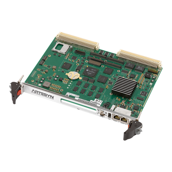
Chapter 3 Controls, LEDs, and Connectors Board Layout The following figure shows the components and the connectors on the MVME2500 board. Figure 3-1 Component Layout MVME2500 Installation and Use (6806800L01L) -
Page 50: Front Panel
Controls, LEDs, and Connectors Front Panel The following components are found on the MVME2500 front panel. Figure 3-2 Front Panel LEDs, Connectors and Switches MVME2500 Installation and Use (6806800L01L) -
Page 51: Reset Switch
Controls, LEDs, and Connectors 3.2.1 Reset Switch The MVME2500 has a single push button switch that has both “abort” and “reset” functions. Pressing the switch for less than three seconds generates an abort interrupt to the P20x0 QorIQ PIC. Holding it down for more than three seconds will generate a hard reset. The VME SYSRESET is generated if the MVME2500 is the VMEbus system controller. -
Page 52: Table 3-1 Front Panel Leds
Controls, LEDs, and Connectors Table 3-1 Front Panel LEDs Label Function Location Color Description USER 1 User Defined Front panel By default Yellow User Software Controllable. Refer to the “User LED Register.” User Software Controllable. Refer to the “User LED Register.” FAIL Board Fail Front panel... -
Page 53: On-Board Leds
Controls, LEDs, and Connectors 3.3.2 On-board LEDs The on-board LEDs are listed below. To view its location on the board, see Figure 3-1 on page Figure 3-4 On-board LEDs Table 3-2 On-board LEDs Status Label Function Color Description Power Fail This indicator is illuminated when one or more of the on- board voltage rails fails. -
Page 54: Front Panel Connectors
Controls, LEDs, and Connectors 3.4.1 Front Panel Connectors The following connectors are found on the outside of the MVME2500 board. These connectors are divided between the front panel connectors and the backplane connectors. The front panel connectors include the J1 and the J5 connectors. The backplane connectors include the P1 and the P2 connectors. -
Page 55: Front Panel Serial Port (J4)
There is one front access asynchronous serial port interface that is routed to the micro mini DB- 9 front panel connector. A male-to-male micro-mini DB9 adapter cable is available under Artesyn part number SERIAL-MINI-D (30-W2400E01A) and ACC/CABLE/SER/DTE/6E 9-pin micro-DSUB to 9-pin DSUB cross connected serial console cable. The pin assignments for these... -
Page 56: Usb Connector (J5)
Controls, LEDs, and Connectors 3.4.1.3 USB Connector (J5) The MVME2500 uses upright USB receptacle mounted in the front panel. Table 3-5 USB Connector (J5) Pin Name Signal Description +5 V Data - Data + Mounting Ground Mounting Ground Mounting Ground Mounting Ground 3.4.1.4 VMEBus P1 Connector... - Page 57 Controls, LEDs, and Connectors Table 3-6 VMEbus P1 Connector (continued) Row A Row B Row C Row D Row Z SYSCLK BGIN3 SYSFAIL BGOUT3 BERR SYSRESET +3.3V (not used) LWORD WRITE AM 5 +3.3V (not used) ADD 23 DTACK AM 0 ADD 24 +3.3V (not used)
-
Page 58: Vmebus P2 Connector
Controls, LEDs, and Connectors Table 3-6 VMEbus P1 Connector (continued) Row A Row B Row C Row D Row Z -12V +12V +12V 3.4.1.5 VMEBus P2 Connector The VME P2 connector is a 160-pin DIN. Row B of the P2 connector provides power to the MVME2500 board and to the upper eight VMEbus address lines and additional 16 VMEbus data lines. -
Page 59: On-Board Connectors
Controls, LEDs, and Connectors Table 3-7 VMEbus P2 Connector (continued) Row A Row B Row C Row D Row Z PMC IO 36 DATA 20 PMC IO 35 GE4_A_LED PMC IO 38 DATA 21 PMC IO 37 Serial 3 TX PMC IO 40 DATA 22 PMC IO 39... -
Page 60: Sata Connector (J3)
Controls, LEDs, and Connectors Table 3-8 Flash Programming Header (P7) (continued) Signal Description Programmer's VCC Master In Slave OUT (MISO) HOLD 0 Keying CLOCK Master OUT Slave IN (MOSI) 3.4.2.2 SATA Connector (J3) The on-board customized SATA connector is compatible with the SATA kit, namely VME- 64GBSSDKIT and IVME7210-MNTKIT. -
Page 61: Pmc Connectors
Controls, LEDs, and Connectors Table 3-9 Custom SATA Connector (J3) (continued) Signal Description Signal Description +3.3V SATA RX + +3.3V +3.3V +3.3V 3.4.2.3 PMC Connectors The MVME2500 supports only one PMC site. It utilizes J14 to support PMC I/O that goes to the RTM PMC. -
Page 62: Table 3-11 Pmc J12 Connector
Controls, LEDs, and Connectors Table 3-10 PMC J11 Connector (continued) Signal Description Signal Description PCI CLK +3.3V AD 15 AD 12 GNT A AD 11 REQ A AD 9 +3.3V AD 31 CBE0 AD 28 AD 6 AD 27 AD 5 AD 25 AD 4 +3.3V... - Page 63 Controls, LEDs, and Connectors Table 3-11 PMC J12 Connector (continued) Signal Description Signal Description JTAG TDO +3.3V JTAG TDI STOP PERR +3.3V SERR BUSMODE2 (Pulled CBE1 +3.3V PCI RESET AD 14 BUSMODE3 (PULLED AD 13 DWN) +3.3V M66EN BUSMODE4 (PULLED AD 10 DWN) AD 8...
-
Page 64: Table 3-12 Pmc J13 Connector
Controls, LEDs, and Connectors Table 3-11 PMC J12 Connector (continued) Signal Description Signal Description AD 18 ACK64 +3.3V AD 16 CBE2 Table 3-12 PMC J13 Connector Signal Description Signal Description AD48 AD 47 CBE7 AD 52 CBE6 AD 45 CBE5 CBE4 +3.3V AD 40... -
Page 65: Table 3-13 Pmc J14 Connector
Controls, LEDs, and Connectors Table 3-12 PMC J13 Connector (continued) Signal Description Signal Description +3.3V AD 35 AD 56 AD 34 AD 55 AD 33 AD 54 AD 53 +3.3V AD 32 AD 51 AD 50 AD 49 Table 3-13 PMC J14 Connector Signal Description Signal Description PMC IO 1... -
Page 66: Jtag Connector (P6)
Controls, LEDs, and Connectors Table 3-13 PMC J14 Connector (continued) Signal Description Signal Description PMC IO 13 PMC IO 45 PMC IO 14 PMC IO 46 PMC IO 15 PMC IO 47 PMC IO 16 PMC IO 48 PMC IO 17 PMC IO 49 PMC IO 18 PMC IO 50... - Page 67 Controls, LEDs, and Connectors Table 3-14 JTAG Connector (P6) (continued) Signal Description Signal Description SPI HOLD 0 SPI CS 0 SPI CLK SPI CS 1 SPI HOLD 1 SPI MOSI SPI MISO SPI VCC SCAN 1 TCK SCAN 1 TDI SCAN 1 TRST SCAN 1 TDO SCAN 1 TMS...
-
Page 68: Cop Connector (P50)
Controls, LEDs, and Connectors Table 3-14 JTAG Connector (P6) (continued) Signal Description Signal Description SCAN 5 TDI SCAN 5 TRST 3.4.2.5 COP Connector (P50) The COP header is used for the CPU debug. The pin assignment is dictated by Freescale and is compatible with the processor’s debugging tool. -
Page 69: Sd Connector (J2)
Controls, LEDs, and Connectors 3.4.2.6 SD Connector (J2) Table 3-16 SD Connector (J2) Signal Description DATA 3 COMMAND VCC (+3.3V) CLOCK DATA 0 DATA 1 DATA 2 WRITE PROTECT CARD DETECT 3.4.2.7 XMC Connector (XJ2) The MVME2500 has one XMC connector (XJ2) that supports XMC cards with J15 connector. It can also support XMC cards with J16 connector without encountering any mechanical interference. -
Page 70: Miscellaneous P2020 Debug Connectors
Controls, LEDs, and Connectors Table 3-17 XMC Connector (XJ2) Pinout (continued) Row A Row B Row C Row D Row E Row F +3.3V +3.3V JTAG TMS +12V +3.3V +3.3V JTAG TMS -12V +3.3V JTAG TDO GA 0 TX0 - BIST TX1 + TX1 -... -
Page 71: Switches
Controls, LEDs, and Connectors Table 3-18 P20x0 Debug Header (continued) Signal Description MSRCDI1 MDVAL MSRCDI2 TRIG_OUT MSRCDI3 TRIG_IN MSRCID4 Switches These switches control the configuration of the MVME2500. Board Malfunction Switches marked as “reserved” might carry production-related functions and can cause ... -
Page 72: Table 3-19 Geographical Address Switch
Controls, LEDs, and Connectors Note that this switch is wired in parallel with the geographical address pins on the 5-row connector. These switches must be in the "OFF" position when installed in a 5-row chassis in order to get the correct address from the P1 connector. This switch also includes the SCON control switches. -
Page 73: Smt Configuration Switch (S2)
Controls, LEDs, and Connectors 3.5.2 SMT Configuration Switch (S2) This eight position SMT configuration switch controls the flash bank write-protect, selects the flash boot image, and controls the safe start ENV settings. The default setting on all switch positions is "OFF" and is indicated by brackets in Table 3-20. - Page 74 Controls, LEDs, and Connectors Table 3-20 Geographical Address Switch Settings (continued) DEFAULT Signal Name Description Notes OFF (Flash Block A) BOOT_BLOCK_A Boot Block B Select The MVME2500 supports dual boot. ON: Flash Block B User can select either Flash OFF: Flash Block A A or Flash B to boot the board.
- Page 75 Controls, LEDs, and Connectors Table 3-20 Geographical Address Switch Settings (continued) DEFAULT Signal Name Description Notes OFF (WP Enabled) MASTER_WP_DISA Write-Protect Disable For I2C write-protect only. BLED switch Switching it "ON" will disable the write-protect. ON: WP disabled OFF: WP enabled OFF (Front) GBE_MUX_SEL User Defined switch that...
- Page 76 Controls, LEDs, and Connectors MVME2500 Installation and Use (6806800L01L)
-
Page 77: Functional Description
Chapter 4 Functional Description Block Diagram The MVME2500 block diagram is illustrated in Figure 4-1. All variants provide front panel access to one serial port via a micro-mini DB-9 connector, two 10/100/1000 Ethernet port (one is configurable to be routed to the front panel or to the rear panel) through a ganged RJ45 connector and one Type A USB port. -
Page 78: Chipset
Functional Description Chipset The MVME2500 utilizes the QorIQ P20x0 integrated processor. It offers an excellent combination of protocol and interface support which includes the following components: The QorIQ P20x0 integrated processor or e500v2 processor core (P2020) and a single e500v2 processor core (P2010). -
Page 79: Integrated Memory Controller
Functional Description 4.2.2 Integrated Memory Controller A fully programmable DDR SDRAM controller supports most JEDEC standard DDR2 and DDR3 memories available. Unbuffered registered DIMMs are also supported. A built-in error checking and correction (ECC) ensures very low bit-error rates for reliable high-frequency operation. Though ECC is not implemented on MVME2500, the board includes a place holder for additional chips for ECC whenever it is needed in the future. -
Page 80: Local Bus Controller (Lbc)
Functional Description 4.2.4 Local Bus Controller (LBC) The main component of the enhanced LBC is the memory controller that provides a 16-bit interface to various types of memory devices and peripherals. The memory controller is responsible for controlling eight memory banks shared by the following: a general purpose chip select machine (GPCM);... -
Page 81: Dma Controller
Functional Description 4.2.9 DMA Controller The DMA controller transfers blocks of data between the various interfaces and functional blocks of P20x0 that are independent of the e500 cores. The P20x0 DMA controller has three high-speed DMA channels, all of which capable of complex data movement and advanced transaction chaining. -
Page 82: Common On-Chip Processor (Cop)
Functional Description 4.2.13 Common On-Chip Processor (COP) The COP is the debug interface of the QorIQ P20x0 processor. It allows a remote computer system to access and control the internal operation of the processor. The COP interface connects primarily through the JTAG and has additional status monitoring signals. The COP has additional features like breakpoints, watch points, register and memory examination/modification and other standard debugging features. -
Page 83: Internal Timer
Functional Description Real-Time Clock Battery, on page 97 for more information on the real time clock back-up battery. 4.4.2 Internal Timer The processor's internal timer is composed of eight global timers divided into two groups of four timers each. Each timer has four individual configuration registers and they cannot be cascaded together. -
Page 84: Spi Bus Interface
Functional Description SPI Bus Interface The enhanced serial peripheral interface (eSPI) allows the device to exchange data with peripheral devices such as EEPROMs, RTC, Flash and the like. The eSPI is a full-duplex synchronous, character-oriented channel that supports a simple interface such as receive, transmit, clock and chip selects. -
Page 85: Firmware Redundancy
Functional Description Factory Pre-Programming the SPI Flash usually takes a while. Ideally, the SPI Flash should be pre-programmed in the factory before shipment. ICT Programming - This programming is done on exposed test points using a bed of nails ... -
Page 86: Figure 4-2 Spi Device Multiplexing Logic
Functional Description The MVME2500 FPGA controls the chip select to SPI devices A and B. The FPGA chip select control is based on the Switch Bank (S2-2). Figure 4-2 SPI Device Multiplexing Logic At power-up, the selection of the SPI boot device is strictly based upon the Switch Bank (S2-2) setting. -
Page 87: Crisis Recovery
The MVME2500 utilizes one of the two UART functions provided in the male micro-mini DB-9 front panel. A male-to-male micro-mini DB-9 to DB9 adapter cable is available under Artesyn Part Number SERIAL-MINI-D (30-W2400E01A) and is approximately 12 inches in length. -
Page 88: Rear Uart Control
Functional Description Only 115200 bps and 9600 bps are supported. The default baud rate on the front panel serial is 9600 kbps. Rear UART Control The MVME2500 utilizes the Exar ST16C554 quad UART (QUART) to provide four additional ports to the RTM. These devices feature 16 bytes of transmit and receive first-in first-out (FIFO) with selectable receive FIFO trigger levels and data rates of up to 1.5 Mbps. -
Page 89: Pmc Add-On Card
Functional Description PMC/XMC sites are keyed for 3.3V PMC signaling. The PMC and the XMC add-on cards must have a hole in the 3.3 V PMC keying position in order to be populated on the MVME2500. The XMC specification accommodates this since it is expected that carrier cards will host both XMC and PMC capable add-on cards. -
Page 90: Sata Interface
Functional Description 4.10 SATA Interface The MVME2500 supports an optional 2.5" SATA HDD. The connector interface is compatible with the SATAMNKIT, which contains the following: one SSD/HDD, one SATA board, screws and a mounting guide. The SATA connector can support a horizontal mounted SSD/HDD. The MVME2500 uses Marvell's 88SE6121B2-NAA2C000 SATA controller and supports up to 1.5 Gbps (SATA Gen 1). -
Page 91: I2C Devices
Functional Description 4.13 I C Devices The MVME2500 utilizes one of the two I2C ports provided by the board's processor. The I C bus is a two-wire, serial data (SDA) and serial clock (SCL), synchronous, multi-master bi-directional serial bus that allows data exchange between this device and other devices such as VPD, SPD, EEPROM, RTC, temperature sensor, RTM, XMC, and IDT clocking. -
Page 92: On-Board Voltage Supply Requirement
Functional Description 4.15.1 On-board Voltage Supply Requirement The on-board power supply is considered to be out of regulation if the output voltage level is below the minimum required power or goes beyond the maximum. Table 4-1 Voltage Supply Requirement Voltage Rail Requirement Voltage Rail Minimum Maximum... -
Page 93: Figure 4-3 Power Up Sequence
Functional Description The figure below describes the detailed power up sequence of the board from +5V (main source from backplane) up to the 1.5 V Power Good. Figure 4-3 Power Up Sequence POWER SEQUENCE DIAGRAM DOCUMENT NUMBER 6306822HA.cpm PAGE 83 OF 87 MVME2500 Installation and Use (6806800L01L) -
Page 94: Clock Structure
Functional Description 4.16 Clock Structure A total of three IDT chips, a discrete oscillator, and crystal supports all the clock requirements of MVME2500. Figure 4-4 Clock Distribution Diagram 4.17 Reset Structure The MVME2500 reset will initiate after the power up sequence if the 1.5 V power supply is “GOOD”. -
Page 95: Reset Sequence
Functional Description 4.17.1 Reset Sequence The timing of the reset sequence supports each chip reset requirements with respect to the power supply. All the resets are controlled by the FPGA with a power supply of +3.3 V from+5 V. All the resets are asserted until +1.5 V power is Good. -
Page 96: Reset Sequence
Functional Description The figure below describes the reset sequence from the +5 V Power Good to the release of the CPU reset. Figure 4-5 Reset Sequence RESET SEQUENCE DOCUMENT NUMBER 6306822HA.cpm PAGE 84 OF 87 MVME2500 Installation and Use (6806800L01L) -
Page 97: Thermal Management
It provides backup power for the on-board RTC when primary power is unavailable. 4.20 Debugging Support The following information shows the details of Artesyn debugging support as applied to the MVME2500. MVME2500 Installation and Use (6806800L01L) -
Page 98: Post Code Indicator
Functional Description 4.20.1 POST Code Indicator The following table shows the LED status of the POST Codes. For the location of the POST Code LEDs, see On-board LEDs, on page Logic 1 = LED is “ON”, Logic 0 = LED is “OFF” Table 4-3 POST Code Indicator on the LED Sequence Description... -
Page 99: Custom Debugging
Functional Description 4.20.3 Custom Debugging Custom debugging makes use of the common on-chip processor. Refer to Common On-Chip Processor (COP), on page 82 for details. 4.21 Rear Transition Module (RTM) The MVME2500 is compatible with the MVME721x RTM. The MVME721X RTM is for I/O routing through the rear of a compact VMEbus chassis. It connects directly to the VME backplane in chassis with an 80 mm deep rear transition area. - Page 100 Functional Description MVME2500 Installation and Use (6806800L01L)
-
Page 101: Memory Maps And Registers
Chapter 5 Memory Maps and Registers Overview System resources including system control and status registers, external timers, and the QUART are mapped into 16 MB address range accessible from the MVME2500 local bus through the P20x0 QorIQ LBC. Memory Map The following table shows the physical address map of the MVME2500. -
Page 102: Flash Memory Map
Memory Maps and Registers Flash Memory Map The table below lists the memory range designated to U-boot and ENV variables. Table 5-2 Flash Memory Map Description Memory Area U-boot 0x00000000 0x0008ffff Reserved 0x00090000 0x0009ffff ENV Variables 0x00100000 0x0011ffff Available Flash 0x00120000 0x007fffff Linux Devices Memory Map The table below lists the memory ranges designated to different devices in Linux. - Page 103 Memory Maps and Registers Table 5-3 Linux Devices Memory Map (continued) Device Memory Range Memory Area Size FPGA 0xffdf0000 0xffdf0fff 4 KB ecm local access window CCSR 0xffe00000 0xffe00ffff 4 KB ecm (Error Correction Module) CCSR 0xffe01000 0xffe01fff 4 KB Memory Controller CCSR 0xffe02000 0xffe02fff 4 KB...
-
Page 104: Programmable Logic Device (Pld) Registers
Memory Maps and Registers Programmable Logic Device (PLD) Registers 5.5.1 PLD Revision Register The MVME2500 provides a PLD revision register that is read by the system software to determine the current version of the timers/registers PLD. Table 5-4 PLD Revision Register PLD Revision Register - 0xFFDF0000 Field PLD Rev... -
Page 105: Pld Month Register
Memory Maps and Registers 5.5.3 PLD Month Register The MVME2500 PLD provides an 8-bit register which contains the build month of the timers/registers PLD. Table 5-6 PLD Month Register PLD Year Register - 0xFFDF0005 Field PLD Rev OPER RESET 5.5.4 PLD Day Register MVME2500 PLD provides an 8-bit register which contains the build day of the timers/registers PLD. -
Page 106: Pld Power Good Monitor Register
Memory Maps and Registers Table 5-8 PLD Sequence Register PLD Revision Register - 0xFFDF0007 Field PLD Rev OPER RESET 5.5.6 PLD Power Good Monitor Register The MVME2500 PLD provides an 8-bit register which indicates the instantaneous status of the supply’s power good signals. Table 5-9 PLD Power Good Monitor Register PLD PWRDG_MNTR - 0xFFDF0012 Field... -
Page 107: Pld Led Control Register
Memory Maps and Registers PWR_V3P3_PWRGD 3.3V Supply power good indicator PWR_V2P5_PWRGD 2.5V Supply power good indicator PWR_V1P2_SW_PWRG 1.2V SW Supply power good indicator PWR_V1P5_PWRGD 1.5V Supply power good indicator 1 - Supply Good and Stable 0 - Otherwise 5.5.7 PLD LED Control Register The MVME2500 PLD provides an 8-bit register which controls the eight LEDs. -
Page 108: Pld Pci/Pmc/Xmc Monitor Register
Memory Maps and Registers 5.5.8 PLD PCI/PMC/XMC Monitor Register The MVME2500 PLD provides an 8-bit register which indicates the status of the PCI/PMC/XMC interface signals. Table 5-11 PLD PCI/PMC/XMC Monitor Register PLD PCI_PMC_XMC_MNTR - 0xFFDF001D Field RSVD RSVD RSVD PMC_X PMC1_E PMC1P_ XMCP1_... -
Page 109: Pld U-Boot And Tsi Monitor Register
Memory Maps and Registers 5.5.9 PLD U-Boot and TSI Monitor Register The MVME2500 PLD provides an 8-bit register which indicates the status of the U-Boot's normal environment switch and TSI interface signals. Table 5-12 PLD U-Boot and TSI Monitor Register PLD PCI_PMC_XMC_MNTR - 0xFFDF001F Field RSVD... -
Page 110: Pld Write Protect And I2C Debug Register
Memory Maps and Registers Table 5-13 PLD Boot Bank Register PLD Boot Bank - 0xFFDF0050 Field SPI_GOODReg BOOT_B BOOT_S LOCK_A (write 0xA4 into this reg to indicate successful loading of the U- Boot. OPER RESET Field Description BOOT_BLOCK_A Boot Block Manual Selector Switch 1 - SPI0 0 - SPI1 BOOT_SPI... - Page 111 Memory Maps and Registers Field Description MASTER_WP_DISABLED I2C devices manual switch write-protect status 1 - Write-protect enabled 0 - Write-protect disabled FLASH_WP_N SPI devices manual switch write-protect status 1 - Write-protect disabled 0 - Write-protect enabled I2C_DEBUG_EN I2C debug ports (I2C_1_D and I2C_1_C) enable 1 - Drive Enabled 0 - Drive Disabled SERIAL_FLASH_WP...
-
Page 112: Pld Test Register 1
Memory Maps and Registers 5.5.12 PLD Test Register 1 The MVME2500 PLD provides an 8-bit general purpose read/write register which is used by the software for PLD testing or general status bit storage. Table 5-15 PLD Test Register 1 PLD Test Register 1- 0xFFDF0080 Field TEST_REG1 OPER... -
Page 113: Pld Gpio2 Interrupt Register
Memory Maps and Registers 5.5.14 PLD GPIO2 Interrupt Register The Abort switch, Tick Timer 0, 1 and 2 interrupts are ORed together. The MVME2500 provides an interrupt register that the system software reads to determine which device the interrupt originated from. GPIO2 will be driven "low" if any of the interrupts asserts. Table 5-17 PLD GPIO2 Interrupt Register PLD Write Protect I2C Debug- 0xFFDF0095 Field... -
Page 114: Pld Shutdown And Reset Control And Reset Reason Register
Memory Maps and Registers 5.5.15 PLD Shutdown and Reset Control and Reset Reason Register The MVME2500 provides an 8-bit register to execute the shutdown and reset commands. The board's reset reason is also included in this register. Table 5-18 PLD Shutdown and Reset Control and Reset Reason Register PLD Shutdown and Reset Reason- 0xFFDF00FF Field AUTO_SH... -
Page 115: Pld Watchdog Timer Refresh Register
Memory Maps and Registers CPU_RESET CPU_HRESET_REQ_L Reset Reason 1 - Reset is due to CPU_HRESET_REQ_L signal 0 -None WD_TIMEOUT Watchdog Timeout Reset Reason 1 - Reset is due to watchdog timing out 0 - None LRSTO TSI LRSTO Reset Reason 1 - Reset is due to LRSTO signal 0 - None Sft_RST... -
Page 116: Pld Watchdog Control Register
Memory Maps and Registers 5.5.17 PLD Watchdog Control Register The MVME2500 provides a watchdog control register. Table 5-20 PLD Watchdog Control Register PLD Watch Dog Timer Load - 0xFFC80604 Field Watchdog_EN RSVD RSVD RSVD RSVD RSVD RSVD RSVD RSVD RSVD RSVD RSVD RSVD... -
Page 117: External Timer Registers
Memory Maps and Registers Field Description Count Count. These bits define the watchdog timer count value. When the watchdog counter is enabled, it will count up from zero (reset value) with a 1 ms resolution until it reaches the COUNT value set by this register. Watchdog will generate a soft reset signal if it bites. -
Page 118: Control Registers
Memory Maps and Registers 5.6.2 Control Registers Table 5-23 Control Registers Tick Timer 0 Control Register - 0xFFC80202 Tick Timer 1 Control Register - 0xFFC80302 Tick Timer 2 Control Register - 0xFFC80402 Field INTS CINT RSVD RSVD RSVD RSVD RSVD ENINT RSVD COVF... -
Page 119: Compare High And Low Word Registers
Memory Maps and Registers 5.6.3 Compare High and Low Word Registers The tick timer counter is compared to the Compare Register. When the values are equal, the tick timer interrupt is asserted and the overflow counter increments. If the clear-on-compare mode is enable, the counter is also cleared. -
Page 120: Counter High And Low Word Registers
Memory Maps and Registers 5.6.4 Counter High and Low Word Registers When enabled, the tick timer counter register increments every microsecond. Software may read or write the counter at any time. Table 5-26 Counter High Word Registers Tick Timer 0 Counter Value High Word - 0xFFC80208 Tick Timer 1 Counter Value High Word - 0xFFC80308 Tick Timer 2 Counter Value High Word - 0xFFC80408 Field... -
Page 121: Boot System
Chapter 6 Boot System Overview The MVME2500 uses Das U-Boot, a boot loader software based on the GNU Public License. It boots the blade and is the first software to be executed after the system is powered on. Its main functions are: Initialize the hardware ... -
Page 122: Boot Options
Boot System U-Boot aborts the boot sequence and enters into a command line interface mode. Enter the command setenv bootdelay -1; saveenv to disable the U-Boot auto-boot feature and let the U-Boot directly enter the command line interface after the next reboot/power up. -
Page 123: Booting From An Optional Sata Drive
Boot System 6.3.2 Booting from an Optional SATA Drive Make sure that the are saved in the SATA drive with ext2 kernel, dtb, ramdisk partition. 2. Configure U-Boot environment variable: setenv File_uImage <kernel_image> setenv File_dtb <kernel dtb> setenv File_ramdisk <ramdisk> saveenv 3. -
Page 124: Booting From An Sd Card
Boot System 6.3.4 Booting from an SD Card Make sure that the , and are saved in the SD card with FAT kernel, dtb ramdisk partition. 2. Configure the U-Boot environment variable: setenv File_uImage <kernel_image> setenv File_dtb <kernel dtb> setenv File_ramdisk <ramdisk> saveenv Initialize SD card: mmcinfo... -
Page 125: Using The Persistent Memory Feature
Boot System 3. TFTP the files from the server to local memory, then boot: run vxboot Using the Persistent Memory Feature The persistent memory means that the RAM's memory is not deleted during a reset. Power cycling, or by temporarily removing the power and then powering up the blade again, will delete the memory content. -
Page 126: Mvme2500 Specific U-Boot Commands
Boot System MVME2500 Specific U-Boot Commands Table 6-1 MVME2500 Specific U-Boot Commands Command Description base Print or set address offset bdinfo Print board info structure boot Boot default, i.e., run 'bootcmd' bootd Boot default, i.e., run 'bootcmd' bootelf Boot from an ELF image in memory bootm Boot application image from memory bootp... - Page 127 Boot System Table 6-1 MVME2500 Specific U-Boot Commands (continued) Command Description help Print online help I2C sub-system iminfo Print header information for application image imxtract Extract a part of a multi-image interrupts Enable or disable interrupts itest Return true/false on integer compare loadb Load binary file over serial line (kermit mode) loads...
-
Page 128: Updating U-Boot
Boot System Table 6-1 MVME2500 Specific U-Boot Commands (continued) Command Description Run commands in an environment variable saveenv Save environment variables to persistent storage script Run a ';' delimited, ';;' terminated list of commands scsi SCSI sub-system scsiboot Boot from SCSI device setenv Set environment variables setexpr... - Page 129 Boot System 3. Select SPI flash # 0: sf probe 0 4. Erase 0x90000 bytes starting at SPI address 0: sf erase 0 0x90000 5. Write 0x90000 bytes from RAM address 0x1000000 starting at SPI address 0: sf write 0x1000000 0 0x90000 To replace the image in SPI bank 1, replace step 2 with Select SPI flash # 1: sf probe 1 MVME2500 Installation and Use (6806800L01L)
- Page 130 Boot System MVME2500 Installation and Use (6806800L01L)
-
Page 131: Programming Model
Chapter 7 Programming Model Overview This chapter includes additional programming information for the MVME2500. Reset Configuration The MVME2500 supports the power-on reset (POR) pin sampling method for processor reset configuration. Each option and the corresponding default setting are described in the following table. - Page 132 Programming Model Table 7-1 POR Configuration Settings (continued) CONFIG CONFIG PINS CONFIG SELECTION REMARKS Boot Sequence LGPL3/LFWP, LGPL5 CFG_BOOT_SEQ[1:0] = BOOT SEQUENCE DISABLED Memory Debug DMA2_DACK0 Debug information from Config the DDR SDRAM controller is driven on the MSPCID and MDVAL signs (default) DDR Debug DMA2_DDONE0...
- Page 133 Programming Model Table 7-1 POR Configuration Settings (continued) CONFIG CONFIG PINS CONFIG SELECTION REMARKS ETSEC2 SGMII LGPL1 eTSEC2 Ethernet Mode interface operates in standard parallel interface mode and uses the TSEC_2’pins (default). ETSEC3 SGMMI TSEC_1588_ALARM eTSEC3 Ethernet Mode _OUT2 interface operates in standard parallel interface mode and uses the TSEC_3’pins...
- Page 134 Programming Model Table 7-1 POR Configuration Settings (continued) CONFIG CONFIG PINS CONFIG SELECTION REMARKS BOOT ROM TSEC1_TXD[6:4], 011X On-chip boot ROM-SPI Location TSEC1_TX_ER configuration (x=0), SDHC (x=1) Host/Agent LWE1/LBS1, The processor acts as the Config LA[18:19] host/root complex for all PCI-E/Serial Rapid IO interfaces (default).
-
Page 135: Interrupt Controller
Programming Model Interrupt Controller The MVME2500 uses the MPC8548E integrated programmable interrupt controller (PIC) to manage locally generated interrupts. Currently defined external interrupting devices and interrupt assignments, along with corresponding edge/levels and polarities, are shown in the following table. Table 7-2 MVME2500 Interrupt List Interrupt Usage Interrupt Line (Schematic) -
Page 136: I2C Bus Device Addressing
Programming Model I2C Bus Device Addressing The following table contains the I2C devices used for the MVME2500 and its assigned device address. Table 7-3 I2C Bus Device Addressing I2C Bus Address Device Function Size Notes 0x50 256 x 8 0x4C ADT 7461 Temperature Sensor 0x68 DS 1375 real-time clock... -
Page 137: Other Software Considerations
Programming Model Table 7-4 PHY Types and MII Management Bus Address (continued) PHY MIIM Ethernet Port Function / Location PHY Types Address TSEC2 Gigabit Ethernet port routed to front or back panel, BCM54616 set by GBE_MUX_SEL in S2 TSEC3 Gigabit Ethernet port routed to back panel BCM54616 Other Software Considerations This section provides programming information in relation to various board components. -
Page 138: Quad Uart
Programming Model 7.6.3 Quad UART The MVME2500 console RS232 port is driven by the UART built into the P20x0 QorIQ chip. Additionally, the MVME2500 has a Quad UART chip which provides four 16550 compatible UART. These additional UARTs are internally accessed through the LBC bus. The Quad UART chip clock input (which is internally divided to generate the baud rate) is 1.8432 MHz. -
Page 139: Clock Distribution
Programming Model XACS Extra Address to chip-select setup 0 - Address to chip-select setup is determined by ORx[ACS] Cycle length in bus clocks 0011 - Three bus clock cycle wait state SETA External address termination 0 - Access is terminated internally by the memory controller unless the external device asserts LGTA earlier to terminate the access. -
Page 140: System Clock
Programming Model Table 7-6 Clock Distribution (continued) Device Clock Signal Frequency Clock Tree Source ICS9FG108 CLK_25MHZ_ICS9FG108 25Mhz ICS83905AGILF +3.3V BCM54616S BP_PHY_25MHZ_CLK 25Mhz ICS83905AGILF +3.3V BCM54616S FP_PHY_25MHZ_CLK 25Mhz ICS83905AGILF +3.3V BCM54616S SW_25MHZ_CLK 25Mhz ICS83905AGILF +3.3V CLK_XMC1 100MHz ICS9FG108 DIFF QorIQ P20x0 SD_REF_CLK 100MHz ICS9FG109... -
Page 141: Real Time Clock Input
Programming Model 7.7.2 Real Time Clock Input The RTC clock input is driven by a 1 MHz clock generated by the FPGA. This provides a fixed clock reference for the QorIQ P20x0 PIC timers which the software can use as a known time reference. - Page 142 Programming Model MVME2500 Installation and Use (6806800L01L)
-
Page 143: Replacing The Battery
Appendix A Replacing the Battery Replacing the Battery The figure below shows the location of the board battery. Figure A-1 Battery Location MVME2500 Installation and Use (6806800L01L) - Page 144 Replacing the Battery The battery provides seven years of data retention, summing up all periods of actual data use. Artesyn therefore assumes that there is usually no need to replace the battery except, for example, in case of long-term spare part handling.
- Page 145 Replacing the Battery Replacement Procedure To replace the battery, proceed as follows: 1. Remove the old battery. 2. Install the new battery with the plus sign (+) facing up. Dispose of the old battery according to your country’s legislation and in an environmentally safe way.
- Page 146 Replacing the Battery MVME2500 Installation and Use (6806800L01L)
-
Page 147: Table B-1 Artesyn Embedded Technologies - Embedded Computing Publications
The publications listed below are referenced in this manual. You can obtain electronic copies of Artesyn Embedded Technologies - Embedded Computing publications by contacting your local Artesyn sales office. For released products, you can also visit our Web site for the latest copies of our product documentation. -
Page 148: Table B-2 Manufacturers' Publications
Related Documentation Manufacturers’ Documents For additional information, refer to the following table for manufacturers’ data sheets or user manuals. As an additional help, a source for the listed document is provided. Please note that while these sources have been verified, the information is subject to change without notice. Table B-2 Manufacturers’... -
Page 149: Related Documentation
Related Documentation Table B-3 Related Specifications (continued) Organization Document IEEE IEEE 802.3 LAN/MAN CSMA/CD Access Method IEEE 802.3-2005 IEEE Standard for a Common Mezzanine Card (CMC) Family IEEE Std 1386-2001 IEEE Standard Physical and Environmental Layers for PCI Mezzanine Cards (PMC) IEEE Std 1386.1-2001 IEEE Standard Test Access Port and Boundary-Scan Architecture IEEE Std 1149.1-2001... - Page 150 Related Documentation MVME2500 Installation and Use (6806800L01L)
- Page 152 Artesyn Embedded Technologies, Artesyn and the Artesyn Embedded Technologies logo are trademarks and service marks of Artesyn Embedded Technologies, Inc. All other product or service names are the property of their respective owners. © 2015 Artesyn Embedded Technologies, Inc.
Need help?
Do you have a question about the MVME2500 Series and is the answer not in the manual?
Questions and answers