
Related Manuals for Artesyn MVME5500


Summary of Contents for Artesyn MVME5500
- Page 1 MVME5500 Single Board Computer Programmer’s Reference Guide P/N: 6806800H16C July 2014...
- Page 2 Artesyn reserves the right to revise this document and to make changes from time to time in the content hereof without obligation of Artesyn to notify any person of such revision or changes.
-
Page 3: Table Of Contents
2.10 VPD and User Configuration EEPROMs ..........40 MVME5500 Single Board Computer Programmer’s Reference Guide (6806800H16C) - Page 4 Related Documentation ............. . . 49 Artesyn Embedded Technologies - Embedded Computing Documentation ....49 Manufacturer’s Documents .
- Page 5 MVME5500 Features Summary ........
- Page 6 List of Tables MVME5500 Single Board Computer Programmer’s Reference Guide (6806800H16C)
-
Page 7: List Of Figures
MVME5500 Block Diagram ........ - Page 8 List of Figures MVME5500 Single Board Computer Programmer’s Reference Guide (6806800H16C)
-
Page 9: About This Manual
The MVME5500 Single Board Computer Programmer’s Reference Guide provides general programming information, including memory maps, interrupts, and register data for the MVME5500 family of boards. This document should be used by anyone who wants general, as well as technical information about the MVME5500 products. - Page 10 Repeated item for example node 1, node 2, ..., node Omission of information from example/command that is not necessary at the time being Ranges, for example: 0..4 means one of the integers 0,1,2,3, and 4 (used in registers) Logical OR MVME5500 Single Board Computer Programmer’s Reference Guide (6806800H16C)
-
Page 11: Summary Of Changes
Table "Supported Model Numbers" on page Table "Processor L3CR Register Assignments" on page Table "L3 Cache Configuration Data" on page 47and Table "Manufacturers’ Documents" on page 6806800H16C July 2014 Re branded to Artesyn template. MVME5500 Single Board Computer Programmer’s Reference Guide (6806800H16C) - Page 12 About this Manual About this Manual MVME5500 Single Board Computer Programmer’s Reference Guide (6806800H16C)
-
Page 13: Board Description And Memory Maps
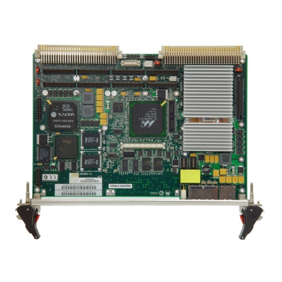
Board Description and Memory Maps Introduction This chapter briefly describes the board level hardware features of the MVME5500 Single Board Computer, including a table of features and a block diagram. The remainder of the chapter provides memory map information including a default memory map, MOTLoad’s processor memory map, a default PCI memory map, MOTLoad’s PCI memory map, a PCI I/O memory... - Page 14 Two PMC sites (one shared with the expansion memory and has IPMC capability) PCI Expansion One expansion connector for interface to PMCspan Miscellaneous Reset/Abort switch Front panel status indicators, Run and Board Fail MVME5500 Single Board Computer Programmer’s Reference Guide (6806800H16C)
- Page 15 Board Description and Memory Maps Table 1-1 MVME5500 Features Summary (continued) Feature Description Form Factor Standard VME Figure 1-1 MVME5500 Block Diagram MVME5500 Single Board Computer Programmer’s Reference Guide (6806800H16C)
-
Page 16: Memory Maps
32 MB PCI Bus 1 Memory Space 3 2A00 0000 F0FF FFFF 3184 MB Unassigned F100 0000 F100 FFFF 64 KB Internal Registers F101 0000 F1FF FFFF 16 MB - Unassigned 64 KB MVME5500 Single Board Computer Programmer’s Reference Guide (6806800H16C) -
Page 17: Motload's Processor Memory Map
F11F FFFF 1 MB GT-64260B Device Bus Registers F120 0000 F1FF FFFF 14 MB Reserved F200 0000 FE00 0000 32 MB Flash Bank 0 FF80 0000 FFFF FFFF 8 MB Flash Bank 1 MVME5500 Single Board Computer Programmer’s Reference Guide (6806800H16C) -
Page 18: Default Pci Memory Map
2200 0000 23FF FFFF 32 MB PCI Bus 0 P2P Memory Space 0 2400 0000 25FF FFFF 32 MB PCI Bus 0 P2P Memory Space 1 2600 0000 F1FF FFFF 32 MB Unassigned MVME5500 Single Board Computer Programmer’s Reference Guide (6806800H16C) -
Page 19: Motload's Pci Memory Maps
PCI 1 Memory Address Start Size Definition 0000 0000 7FFF FFFF 2 GB Onboard SDRAM E000 0000 EFFF FFFF 1 GB Local PCI 1 Domain Memory Space F000 0000 FFFF FFFF 256 MB Reserved MVME5500 Single Board Computer Programmer’s Reference Guide (6806800H16C) -
Page 20: Pci I/O Space Maps
1.3.6 System I/O Memory Map System resources for the MVME5500 board including system control and status registers, NVRAM/RTC, and the 16550 UARTs are mapped into a 1 MB address range assigned to device bank 1. The region defined by device bank 1 resides within the GT-64260B device bus register’s... -
Page 21: System Status Register 1
Reserved (undefined) 1.3.7 System Status Register 1 The MVME5500 board system status register 1 is used to provide board status information and software control of Abort. Table 1-10 System Status Register 1 System Status Register 1 - Offset 0x0 0000... -
Page 22: System Status Register 2
A set condition indicates that all fuses are functional. 1.3.8 System Status Register 2 The MVME5500 board system status register 2 provides board control and status bits. Table 1-11 System Status Register 2 System Status Register 2 - Offset 0x0 0001 FIELD... - Page 23 PCI Bus 0.1 M66EN. This bit reflects the state of the PCI Bus 0.1 M66EN pin. A cleared condition indicates that PCI Bus 0.0 is operating at 33 MHz. A set condition indicates that the bus is operating at 66 MHz. This bit is always cleared on the MVME5500. PCI1.0_M66EN PCI Bus 1.0 M66EN.
-
Page 24: System Status Register 3
OPER RESET BRD_RST Board reset. Setting this bit forces a hard reset of the MVME5500 board. This bit clears automatically when the board reset is complete. ABT_INT_MASK Abort interrupt mask. This bit is used to mask the abort interrupt. If this bit is set, the abort interrupt is masked so the abort interrupt is not generated. -
Page 25: Configuration Header/Switch Register (S1)
PMC module 1 present. If set, there is no PMC module installed in position 1. If cleared, the PMC module is installed. 1.3.11 Configuration Header/Switch Register (S1) The MVME5500 board has an 8-bit header or switch that may be read by the software. Table 1-14 Configuration Header/Switch Register Configuration Header/Switch Register - Offset 0x0 0005h... -
Page 26: Time Base Enable Register
OPER RESET TBEN0 Processor time base enable. When this bit is cleared, the TBEN pin of the processor is driven low. When this bit is set, the TBEN pin is driven high. MVME5500 Single Board Computer Programmer’s Reference Guide (6806800H16C) -
Page 27: Geographical Address Register (S2)
Configuration Header/Switch Register (S1) on page 25) to assign a geographical address according to the following diagram. The switch positions must all be turned off when the MVME5500 is used in a 5-row backplane. Table 1-16 Geographical Address Register Geographical Address Register - 0xFF100007... -
Page 28: Com1 & Com2 Universal Asynchronous Receiver/Transmitter (Uart)
For additional programming details, refer to the PC16550 Data Sheet. 1.3.15 Real-Time Clock and NVRAM The SGS-Thomson M48T37 is used by the MVME5500 board to provide 32 KB of non-volatile static RAM, real-time clock, and watchdog timer functions. The device is accessed as linear memory. -
Page 29: Programming Details
Chapter 2 Programming Details Introduction This chapter includes additional programming information for the MVME5500 Single Board Computer. Items discussed include: PCI Configuration Space and IDSEL Mapping on page 30 Interrupt Controller on page 31 Two-Wire Serial Interface on page 33 ... -
Page 30: Pci Configuration Space And Idsel Mapping
Table 2-1 shows the IDSEL assignments for the PCI devices on each of the PCI buses on the MVME5500 board along with the corresponding interrupt assignment to the general-purpose port (GPP) pins. Refer to the GT-64260B System Controller for PowerPC Processors Data Sheet and the PCI 6154 (HB2) PCI-to-PCI Bridge Data Book, both listed... -
Page 31: Interrupt Controller
Programming Details Interrupt Controller The MVME5500 uses the GT-64260B interrupt controller to handle interrupts internal to the GT-64260B, as well as the external interrupt sources. The GT-64260B has a limited number of directly triggerable interrupt inputs. Each of the GPP pins can be configured for an interrupt input, but the inputs are combined internally in groups of eight inputs (one for each byte lane) for one interrupt source. - Page 32 Watchdog Timer Expired Output WDE# GT-64260B SROM Initialization Active InitAct Level Not Used. Pulled High. Not Used. Pulled High. Optional External PPC Bus Arbiter BG1 Enable Unused. Pulled High. Unused. Pulled High. MVME5500 Single Board Computer Programmer’s Reference Guide (6806800H16C)
-
Page 33: Two-Wire Serial Interface
VPD EEPROM contained on the MVME5500 board, along with the SPD EEPROMs, to further initialize the memory controller and other interfaces. For additional details regarding the GT-64260B... -
Page 34: Gt-64260B Initialization
After reset, all GPP pins default to general-purpose inputs. Software must then configure each of the pins for the desired function. The following table defines the function assigned to each GPP pin on the MVME5500 board. Table 2-4 GT-64260B GPP Pin Function Assignments... - Page 35 Watchdog Timer NMI Output WDNMI# to GPP6 Watchdog Timer Expired Output WDE# GT-64260B SROM Initialization Active InitAct Not Used. Pulled high, tied to GPP4. Not Used. Pulled high, tied to GPP5. Optional external PPC Bus Arbiter BG1 Enable. MVME5500 Single Board Computer Programmer’s Reference Guide (6806800H16C)
-
Page 36: Gt-64260B Reset Configuration
C bus The MVME5500 board supports both options listed above. An onboard jumper setting is used to select the option. If the pin-sample-only method is selected, then states of the various pins on the device AD bus are sampled when reset is deasserted to determine the desired operating modes. -
Page 37: Table 2-5 Gt-64260B Power-Up Configuration Settings
0000 Reserved Must be Pulled Down AD[23] Fixed SDClkIn/SDClkOut Select SDClkIn AD[24] Resistor Internal Space Default Address 0xf100.0000 AD[27:25] Fixed Reserved Must be Pulled Down AD[28] Resistor PLL Tune Tuning Option 0 MVME5500 Single Board Computer Programmer’s Reference Guide (6806800H16C) - Page 38 Device AD Select Power-Up Bus Signal Options Settings Description State of Bit vs. Function AD[29] Resistor PLL Divider Divider Option 0 AD[30] Resistor PLL Bypass PLL Enabled AD[31] Fixed CPU Interface Voltage 2.5V MVME5500 Single Board Computer Programmer’s Reference Guide (6806800H16C)
-
Page 39: Gt-64260B Device Controller Bank Assignments
Programming Details GT-64260B Device Controller Bank Assignments The MVME5500 board uses three of the GT-64260B device controller banks for interfacing to various devices. The following tables define the device bank assignments and the programmable device bank timing parameters required for each of the banks used. Note that all device bank timing parameters, except BAdrSkew, have an extension bit that forms the most significant bit of the timing parameter. -
Page 40: System Clock Generators
2.10 VPD and User Configuration EEPROMs The MVME5500 board contains an Atmel AT24C64 vital product data (VPD) EEPROM containing configuration information specific to the board. Typical information that may be present in the VPD is: manufacturer, board revision, build version, date of assembly, memory present, options present, L3 cache information, etc. -
Page 41: Temperature Sensor
Programming Details 2.11 Temperature Sensor The MVME5500 board contains a Maxim DS1621 digital temperature sensor with an I C serial bus interface. This device may be used to provide a measure of the ambient temperature of the board. 2.12 Flash Memory The MVME5500 contains two banks of Flash memory accessed via the device controller contained within the GT-64260B. -
Page 42: Other Software Considerations
The processor internal clock frequency (core frequency) is a multiple of the system bus frequency. The processor has five configuration pins, PLL_EXT and PLL_CFG[0:3], for hardware strapping of the processor core frequency (between 2x and 16x of the system bus frequency). MVME5500 Single Board Computer Programmer’s Reference Guide (6806800H16C) -
Page 43: L1, L2, L3 Cache
The processors support on-chip L1 and L2 caches and external L3 cache. L3 cache supports 1 or 2 MB in a variety of SRAM device types. Each processor L3 interface on the MVME5500 consists of two 8 Mb devices providing a total of 2 MB of L3 cache. Data parity checking should be enabled. - Page 44 Programming Details MVME5500 Single Board Computer Programmer’s Reference Guide (6806800H16C)
-
Page 45: Vital Product Data
FMC_BANK Bank Number of Flash Memory Array: 0 for this bank FMC_SPEED ROM Access Speed in Nanoseconds FMC_SIZE Total Bank Size (Should agree with the physical organization above): 07 = 32M MVME5500 Single Board Computer Programmer’s Reference Guide (6806800H16C) -
Page 46: Table A-2 Flash 1 Memory Configuration Data
Bank Number of Memory Array: 1 for this bank FMC_SPEED ROM Access Speed in Nanoseconds FMC_SIZE Total Bank Size (Should agree with the physical organization above): 03 = 2M for this bank MVME5500 Single Board Computer Programmer’s Reference Guide (6806800H16C) -
Page 47: L3 Cache Configuration Data
SRAM clock control: 00 - SRAM clock control disabled SRAM type: 03 - SDR SRAM Data bus error detection type: 01 - parity Address bus error detection type: 00 - None MVME5500 Single Board Computer Programmer’s Reference Guide (6806800H16C) - Page 48 Vital Product Data MVME5500 Single Board Computer Programmer’s Reference Guide (6806800H16C)
-
Page 49: Related Documentation
The publications listed below are referenced in this manual. You can obtain electronic copies of Artesyn Embedded Technologies - Embedded Computing publications by contacting your local Artesyn sales office. For released products, you can also visit our Web site for the latest copies of our product documentation. -
Page 50: Manufacturer's Documents
MV-S100414-00B Marvell Technologies, Ltd. Web Site: http://www.marvell.com Intel 82545GM Gigabit Ethernet Controller with Integrated PHY Data 82545GM.pdf Sheet Intel Corporation Literature Center 19521 E. 32nd Parkway Aurora CO 80011-8141 Web Site: http://www.intel.com/design/litcentr/index.htm MVME5500 Single Board Computer Programmer’s Reference Guide (6806800H16C) - Page 51 PCI 6154 (HB2) PCI-to-PCI Bridge Data Book 6154_DataBook_v2.0.p PLX Technology, Inc. 870 Maude Avenue Sunnyvale, California 94085 Web Site: http://www.hintcorp.com/products/hint/default.asp TL16C550C Universal Asynchronous Receiver/Transmitter SLLS177E Texas Instruments P. O. Box 655303 Dallas, Texas 75265 Web Site: http://www.ti.com MVME5500 Single Board Computer Programmer’s Reference Guide (6806800H16C)
-
Page 52: Related Specifications
Table B-3 Specifications Document Title and Source Publication Number VITA http://www.vita.com/ VME64 Specification ANSI/VITA 1-1994 VME64 Extensions ANSI/VITA 1.1-1997 2eSST Source Synchronous Transfer VITA 1.5-199x PCI Special Interest Group (PCI SIG) http://www.pcisig.com/ MVME5500 Single Board Computer Programmer’s Reference Guide (6806800H16C) - Page 53 Related Documentation Table B-3 Specifications (continued) Document Title and Source Publication Number Peripheral Component Interconnect (PCI) PCI Local Bus Specification Local Bus Specification, Revision 2.0, 2.1, 2.2 MVME5500 Single Board Computer Programmer’s Reference Guide (6806800H16C)
- Page 54 Related Documentation MVME5500 Single Board Computer Programmer’s Reference Guide (6806800H16C)
-
Page 55: Safety Notes
Artesyn and our suppliers take significant steps to make sure that there are no bent pins on the backplane or connector damage to the boards prior to leaving the factory. Bent pins caused by improper installation or by inserting boards with damaged connectors could void the Artesyn warranty for the backplane or boards. - Page 56 When exchanging the on-board lithium battery, make sure that the new and the old battery are exactly the same battery models. If the respective battery model is not available, contact your local Artesyn sales representative for the availability of alternative officially approved battery models.
-
Page 57: Sicherheitshinweise
Verletzungen oder Schäden am System zur Folge haben. Artesyn ist darauf bedacht, alle notwendigen Informationen zum Einbau und zum Umgang mit dem System in diesem Handbuch bereit zu stellen. Da es sich jedoch bei dem System um ein komplexes Produkt mit vielfältigen Einsatzmöglichkeiten handelt, können wir die... - Page 58 Sie sicher, dass ausreichend Schutz vor Störstrahlung vorhanden ist. Die Blades müssen mit der Frontblende installiert und alle freien Steckplätze müssen mit Blindblenden abgedeckt sein. Änderungen, die nicht ausdrücklich von Artesyn erlaubt sind, können Ihr Recht das System zu betreiben zunichte machen. MVME5500 Single Board Computer Programmer’s Reference Guide (6806800H16C)
- Page 59 Wenn Sie die Lithium-Batterie auf dem Produkt austauschen, stellen Sie sicher, dass die alte und die neue Batterie vom gleichen Typ sind. Ist der Batterietyp nicht verfügbar, wenden Sie sich an Artesyn um herauszufinden, welcher Batterietyp offiziell alternativ verwendet werden darf.
- Page 60 Sicherheitshinweise MVME5500 Single Board Computer Programmer’s Reference Guide (6806800H16C)
- Page 62 Artesyn Embedded Technologies, Artesyn and the Artesyn Embedded Technologies logo are trademarks and service marks of Artesyn Embedded Technologies, Inc. All other product or service names are the property of their respective owners. © 2014 Artesyn Embedded Technologies, Inc.
Need help?
Do you have a question about the MVME5500 and is the answer not in the manual?
Questions and answers