Table of Contents
Advertisement
Quick Links
Advertisement
Table of Contents

Related Manuals for Artesyn MVME8105


Summary of Contents for Artesyn MVME8105
- Page 1 MVME8100/MVME8105/MVME8110 Programmer’s Reference P/N: 6806800P28H April 2019...
- Page 2 Artesyn reserves the right to revise this document and to make changes from time to time in the content hereof without obligation of Artesyn to notify any person of such revision or changes.
-
Page 3: Table Of Contents
C Devices ............... . 37 MVME8100/MVME8105/MVME8110 Programmer’s Reference (6806800P28H) - Page 4 Artesyn Embedded Technologies Documentation ........
- Page 5 Block Diagram of MVME8105 ........
- Page 6 List of Figures MVME8100/MVME8105/MVME8110 Programmer’s Reference (6806800P28H)
- Page 7 Artesyn Embedded Technologies Publications ........
- Page 8 List of Tables MVME8100/MVME8105/MVME8110 Programmer’s Reference (6806800P28H)
-
Page 9: About This Manual
Chapter 5, Boot System on page 39, provides information on the U-boot. Appendix A, Related Documentation on page 47, provides a listing of related Artesyn Embedded Technologies manuals, vendor documentation, and industry specifications. Abbreviations This document uses the following abbreviations:... - Page 10 Screen body text Used to characterize user input and to separate it from system output Courier + Bold Reference Used for references and for table and figure descriptions File > Exit Notation for selecting a submenu MVME8100/MVME8105/MVME8110 Programmer’s Reference (6806800P28H)
- Page 11 Indicates a hazardous situation which, if not avoided, could result in death or serious injury. Indicates a hazardous situation which, if not avoided, may result in minor or moderate injury. Indicates a property damage message. Helpful information and tips. MVME8100/MVME8105/MVME8110 Programmer’s Reference (6806800P28H)
-
Page 12: Summary Of Changes
Summary of Changes Part Number Publication Date Description Updated to new Artesyn format; minor grammar and formatting updates throughout document; converted bulleted lists of features into a comparison table; Freescale 6806800P28H April 2019 changed to NXP. Removed Board Variants and Board Accessories tables;... -
Page 13: Introduction
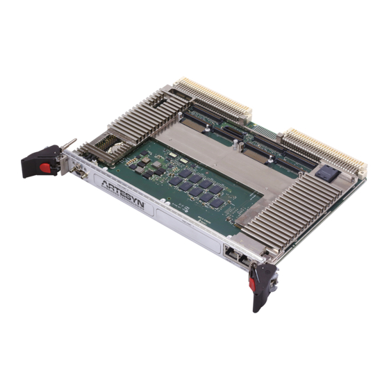
The MVME8100 can accommodate two PCI/PCI Express Mezzanine Cards (PMC/XMC). The MVME8105 is a dual core non‐VXS version of the MVME8100 board based on the NXP QorIQ P5020 processor. It runs at 2.0GHz with 4GB DDR3. The MVME8105 provides a second 1000Base-TX RJ-45 interface on the front panel. -
Page 14: Feature Summary
High-speed USB 2.0 controllers with integrated PHYs CoreNet platform cache with ECC 2Mbyte 2Mbyte 1Mbyte SATA 2.0 controller RAID5/6 engine SEC encryption System Memory DDR3 SDRAM with ECC DDR3 data rate 1333MT/s 1333MT/s 1200MT/s SMBus MVME8100/MVME8105/MVME8110 Programmer’s Reference (6806800P28H) -
Page 15: Table
USB 2.0 for backplane RTM I/O Ethernet 10/100/1000BASE-T Ethernet port to front panel 10/100/1000BASE-T Ethernet channels to P2/RTM 1000BASE-BX Ethernet SERDES channels to P0 backplane/RTM SATA Ports SATA Gen 3 ports to P0 backplane/RTM Serial Ports MVME8100/MVME8105/MVME8110 Programmer’s Reference (6806800P28H) -
Page 16: Table
Front panel RJ-45 connector with integrated LEDs for 10/100/1000 Ethernet channel PMC/XMC Site 1 front I/O and rear PMC I/O PMC/XMC Site 2 front I/O Serial ports to P2/RTM, (two Micro DB-9 connectors on RTM panel and two on planar headers) MVME8100/MVME8105/MVME8110 Programmer’s Reference (6806800P28H) -
Page 17: Ordering And Support Information
ENP4 (conduction cooled) variant are accessed through P2 only Ordering and Support Information The data sheets for the MVME8100, MVME8105 and MVME8110 boards contain a complete list of available variants and accessories. Refer to Appendix A Related Documentation or consult your local Artesyn sales representative for the availability of product variants. -
Page 18: Block Diagram
Introduction Introduction Block Diagram The block diagrams for MVME8100/MVME8105/MVME8110 SBC are shown in the following figures: Figure 1-1 Block Diagram of MVME8100 Front Panel NOTE: Front panel connectors are not assembled on conduction - cooled RESET variant . P 4I/O... - Page 19 Introduction Figure 1-2 Block Diagram of MVME8105 Front Panel M i c r o Dua l Reset PM C /XM C I / O 1 PM C /XM C I / O 2 DB09 R J45 P4 I/O PM C /XM C /2. 5"...
-
Page 20: Figure 1-3 Block Diagram Of Mvme8110
Introduction Introduction Figure 1-3 Block Diagram of MVME8110 MVME8100/MVME8105/MVME8110 Programmer’s Reference (6806800P28H) -
Page 21: Memory Maps
Chapter 2 Memory Maps Overview This chapter provides the memory mapping addresses for the MVME8100, MVME8105 and MVME8110 boards. Refer to the P5020/P5010 Reference Manual for additional details and/or programming information. Memory Maps The following table shows the suggested local memory address map of the P5010/P5020... - Page 22 Memory Maps Memory Maps NOTES MVME8100/MVME8105/MVME8110 Programmer’s Reference (6806800P28H)
-
Page 23: Register Descriptions
Chapter 3 Register Descriptions Overview This chapter describes the various registers on the MVME8100/MVME8105/MVME8110 boards. CPLD Registers For the Complex Programmable Logic Device (CPLD) register description, the convention shown in the following tables are used. Table 3-1 Register Defaults... -
Page 24: Enhanced Local Bus Register
Tick Timer3 Compare Registers 0x38 Tick Timer3 Counter Registers 0x40 Tick Timer4 Control Register 0x44 Tick Timer4 Compare Registers 0x48 Tick Timer4 Counter Registers 0x50 Tick Timer Prescaler Registers 0x60 RTM GPIO Registers 0x80 Scratch Register MVME8100/MVME8105/MVME8110 Programmer’s Reference (6806800P28H) -
Page 25: Identification Register
Note: Register state bits directly reflect logic level applied at pins 20:21 LBC:r BOARDREV (ex. 2'b01 for rev1.1). This will be used for backward compatibility. Board Identification Register 22:31 10'h007: MVME8100 10'b007 LBC:r Others: Reserved for future boards MVME8100/MVME8105/MVME8110 Programmer’s Reference (6806800P28H) -
Page 26: Cpld Command/Status Register
IWD Reset indication 1: IWD Reset has not generated reset 1'b1 LBC:r 0: IWD Reset has generated reset OSWD Reset indication 1: OSWD Reset has not generated reset 1'b1 LBC:r 0: OSWD Reset has generated reset MVME8100/MVME8105/MVME8110 Programmer’s Reference (6806800P28H) - Page 27 1: Enabled (Load Root Complex based EEPROM into PCIe and SRIO switches) LBC:r 0: Disabled (Load Endpoint based EEPROM into PCIe and SRIO switches) Note: The bit reflects SW4-2 setting sampled at reset. (SRIO for MVME8100 only) MVME8100/MVME8105/MVME8110 Programmer’s Reference (6806800P28H)
- Page 28 Note: The bit reflects SW2-8 setting sampled at reset (P0 and SRIO for MVME8100 only) XMC1 Detect 1: Not Present LBC:r 0: Present XMC2 Detect 1: Not Present LBC:r 0: Present PMC1 Detect 1: Not Present LBC:r 0: Present PMC2 Detect 1: Not Present LBC:r 0: Present MVME8100/MVME8105/MVME8110 Programmer’s Reference (6806800P28H)
- Page 29 LBC:r 0: Serial Port 0 Operates in RS-485/422 Mode (SW2-3 closed) Serial Port 1 Mode 1: Serial Port 1 Operates in RS-232 Mode (SW2-4 open) LBC:r 0: Serial Port 1 Operates in RS-485/422 Mode (SW2-4 closed) MVME8100/MVME8105/MVME8110 Programmer’s Reference (6806800P28H)
-
Page 30: User Led Control Register
User LED 1A (front panel USER 1 bicolor LED, yellow) 1: On LBC:r/w 0: Off User LED 1B (front panel USER 1 bicolor LED, red) 1: On LBC:r/w 0: Off User LED 2 (back side D19 bicolor LED, red) 1: On LBC:r/w 0: Off MVME8100/MVME8105/MVME8110 Programmer’s Reference (6806800P28H) -
Page 31: Cpld Build Code Register
Offset: 0x0C Description Default Access Two digit build year (BCD) 8'hxx LBC:r 8:15 Two digit build month (BCD) 8'hxx LBC:r 16:23 Two digit build day (BCD) 8'hxx LBC:r 24:31 Two digit sequence number (BCD) 8'hxx LBC:r MVME8100/MVME8105/MVME8110 Programmer’s Reference (6806800P28H) -
Page 32: Tick Timer Register
A value of "1" in this bit indicates that a interrupt has been generated by 1'b0 LBC:r the corresponding timer. A value of "0" indicates that no interrupt has been generated by the corresponding timer. 21'h00_ 11:31 Reserved LBC:r 0000 MVME8100/MVME8105/MVME8110 Programmer’s Reference (6806800P28H) -
Page 33: Table 3-9 Tick Timer Compare Register
When programming the tick timer for periodic interrupt, the counter should be cleared to zero by software and then enabled. If the counter does not initially start at zero, the time to the first interrupt may be longer or shorter than expected. MVME8100/MVME8105/MVME8110 Programmer’s Reference (6806800P28H) -
Page 34: Rtm Gpio Register
Table 3-13 Scratch Register Offset: 0x80 Description Default Access The Sticky Scratch Register (SSCR) is a 4-byte register that is intended for 0:31 LBC:r/w the programmer's use as a scratch pad and reset only by power cycle. MVME8100/MVME8105/MVME8110 Programmer’s Reference (6806800P28H) -
Page 35: Programming Model
Chapter 4 Programming Model Overview This chapter provides programming information for MVME8100/MVME8105/MVME8110 boards. Interrupt Controller Assignments The following table shows the external interrupts connected to the P5020/P5010 processors. Table 4-1 P5020 External Interrupt Assignments P5020 Interrupt Interrupt Source Description... -
Page 36: Ethernet Phy Management Addresses
00010 RTM GIGE3 BCM54616S 00011 Note: For MVME8105, RTM GIGE4 is GENET2 and Front Panel ETH is GENET1. Local Bus Controller Chip select Assignment The following table shows the devices connected to the P5020/P5010 LBC bus chip select. Table 4-3... -
Page 37: I 2 C Devices
XMC 2 0x52(0xA4) XMC dependent SRIO (only for MVME8100) Switch Alternate 0x54(0xA8) AT24C64D Configuration EEPROM1 SRIO (only for MVME8100) Switch Primary 0x55(0xAA) AT24C64D Configuration EEPROM1 SRIO (only for MVME8100) 0x5D(0xBA) 80HCPS1616 Switch I C Slave Interface MVME8100/MVME8105/MVME8110 Programmer’s Reference (6806800P28H) - Page 38 Selection of Primary and Alternate Configuration EEPROM is determined by PCIe/SRIO (only for MVME8100) Root Complex/Endpoint switch S4-2. For more information, refer to the S4 Switch section in the MVME8100/MVME8105/MVME8110 Installation and Use Manual. MVME8100/MVME8105/MVME8110 Programmer’s Reference (6806800P28H)
-
Page 39: Boot System
Boot System Overview The MVME8100/MVME8105/MVME8110 boards use Das U-Boot, a boot loader software based on the GNU Public License. It boots the board and is the first software to be executed after the system is powered on. Its main functions are: Initialize the hardware ... -
Page 40: Boot Options
3. Transfer the files through the TFTP from the server to the local memory. tftpboot 1000000 kernel_image> tftpboot 2000000 <ramdisk> tftpboot F00000 <kernel dtb> 4. Boot the Linux from the memory. bootm 1000000 2000000 f00000 MVME8100/MVME8105/MVME8110 Programmer’s Reference (6806800P28H) -
Page 41: Booting From An Optional Sata Drive
1. Make sure that the following are saved in the USB drive with FAT partition: kernel ramdisk 2. Configure the U-Boot environment variable: setenv bootfile <kernel_image> setenv dtbfile <kernel dtb> setenv ramdiskfile <ramdisk> saveenv 3. Initialize USB drive: usb reset (’USB reset 1’ for RTM USB) MVME8100/MVME8105/MVME8110 Programmer’s Reference (6806800P28H) -
Page 42: Booting From Mmc
5.3.5 Booting VxWorks Through the Network In this mode, the U-Boot downloads and boots VxWorks from an external TFTP server. 1. Make sure that the VxWorks image is accessible by the board from the TFTP server. MVME8100/MVME8105/MVME8110 Programmer’s Reference (6806800P28H) -
Page 43: Mvme8100/Mvme8105/Mvme8110 Specific U-Boot Commands
For more information on bootline configuration/usage, refer to the VxWorks Kernel Programmer’s Guide. 3. TFTP the files from the server to local memory, then boot: run vxboot MVME8100/MVME8105/MVME8110 Specific U-Boot Commands Table 5-1 MVME8100/MVME8105/MVME8110 Specific U-Boot Commands Command Description Print or set address offset base Print board info structure bdinfo Boot default, i.e., run 'bootcmd'... - Page 44 Boot System Boot System Table 5-1 MVME8100/MVME8105/MVME8110 Specific U-Boot Commands (continued) Command Description Memory copy Multiprocessor CPU boot manipulation and release Checksum calculation crc32 Get/set/reset date & time date Boot image via network using DHCP/TFTP protocol dhcp Runs POST diags...
- Page 45 Boot System Table 5-1 MVME8100/MVME8105/MVME8110 Specific U-Boot Commands (continued) Command Description Load S-Record file over serial line loads Load binary file over serial line (ymodem mode) loady Infinite loop on address range loop Display and program the system ID and MAC addresses...
-
Page 46: Updating U-Boot
Boot System Boot System Table 5-1 MVME8100/MVME8105/MVME8110 Specific U-Boot Commands (continued) Command Description Run script from memory source Minimal test like /bin/sh test Boot image through network using TFTP protocol tftpboot Initialize and configure Tundra Tsi148 tsi148 USB sub-system... -
Page 47: Related Documentation
The publications listed below are referenced in this manual. You can obtain electronic copies of Artesyn Embedded Technologies publications by contacting your local Artesyn sales office. For released products, you can also visit our Web site for the latest copies of our product documentation. -
Page 48: Related Specifications
April 27, 2000 PCI Special Interest Group PCI Rev 2.2 PCI Local Bus Specification, Revision 2.2 December 18, 1998 PCI-X Electrical and Mechanical Addendum to the PCI Local Bus PCI-X EM 2.0a Specification, Revision 2.0a August 22, 2003 MVME8100/MVME8105/MVME8110 Programmer’s Reference (6806800P28H) -
Page 49: Manufacturers' Documents
Document Title and Source Publication Number NXP Semiconductors P5020/P5010 QorIQ Integrated Processor Hardware Specifications P5020EC P5020RM P5020 QorIQ Integrated Multicore Communication Processor Reference Manual Integrated Device Technology IDT 89HPES32NT24xG2 PCI Express Switch User Manual CPS-1616 Central Packet Switch Datasheet MVME8100/MVME8105/MVME8110 Programmer’s Reference (6806800P28H) - Page 50 Related Documentation Related Documentation NOTES MVME8100/MVME8105/MVME8110 Programmer’s Reference (6806800P28H)
- Page 52 Artesyn Embedded Technologies, Artesyn and the Artesyn Embedded Technologies logo are trademarks and service marks of Artesyn Embedded Technologies, Inc. All other product or service names are the property of their respective owners. ©2019 Artesyn Embedded Technologies, Inc.
Need help?
Do you have a question about the MVME8105 and is the answer not in the manual?
Questions and answers