Table of Contents
Advertisement
Quick Links
Advertisement
Table of Contents

Subscribe to Our Youtube Channel
Related Manuals for Artesyn MVME2500-ECC


Summary of Contents for Artesyn MVME2500-ECC
- Page 1 MVME2500-ECC Installation and Use P/N: 6806800N30G May 2016...
- Page 2 Artesyn reserves the right to revise this document and to make changes from time to time in the content hereof without obligation of Artesyn to notify any person of such revision or changes.
-
Page 3: Table Of Contents
3.3.1 Front Panel LEDs ............. 51 MVME2500-ECC Installation and Use (6806800N30G) - Page 4 4.2.11 General Purpose I/O (GPIO)........... . 78 MVME2500-ECC Installation and Use (6806800N30G)
- Page 5 4.20.1 POST Code Indicator............92 MVME2500-ECC Installation and Use (6806800N30G)
- Page 6 Overview ............... . . 117 MVME2500-ECC Installation and Use (6806800N30G)
- Page 7 MVME2500-ECC Specific U-Boot Commands ........
- Page 8 Related Specifications ............. . 144 MVME2500-ECC Installation and Use (6806800N30G)
- Page 9 Key Features of the MVME2500-ECC ........
- Page 10 MVME2500-ECC Specific U-Boot Commands ........122...
- Page 11 MVME2500-ECC SCANBE Board ........
- Page 12 List of Figures MVME2500-ECC Installation and Use (6806800N30G)
-
Page 13: About This Manual
Abbreviations This document uses the following abbreviations: Term Definition CPLD Complex Programmable Logic Device DDR3 Double Data Rate 3 DUART Dual Universal Asynchronous Receiver Transmitter EEPROM Erasable Programmable Read-Only Memory MVME2500-ECC Installation and Use (6806800N30G) - Page 14 PCI Mezzanine Card (IEEE P1386.1) PrPMC Processor PCI Mezzanine Card Real-Time Clock Rear Transition Module SATA Serial Advanced Technology Attachment UART Universal Asynchronous Receiver-Transmitter VITA VMEbus International Trade Association Versa Module Eurocard PCI eXpress Mezzanine Card MVME2500-ECC Installation and Use (6806800N30G)
- Page 15 Repeated item for example node 1, node 2, ..., node Omission of information from example/command that is not necessary at the time being Ranges, for example: 0..4 means one of the integers 0,1,2,3, and 4 (used in registers) Logical OR MVME2500-ECC Installation and Use (6806800N30G)
- Page 16 Updated Boot Options and Crisis Recovery. 6806800N30F August 2014 Re-branded to Artesyn template. Added Declaration of Conformity on page24. 6806800N30E December 2013 Updated Chapter 4, PMC Add-on Card, on page 86 Chapter 5, PLD PCI/PMC/XMC Monitor Register, on page 101. MVME2500-ECC Installation and Use (6806800N30G)
- Page 17 Description, Chapter 5, Programmable Logic Device (PLD) Registers Chapter 5, PLD Boot Bank Register, on page 103. 6806800N30C January 2013 Updated Standard Compliances on page 6806800N30B May 2012 ECC-related updates 6806800N30A November 2011 First edition MVME2500-ECC Installation and Use (6806800N30G)
- Page 18 About this Manual About this Manual MVME2500-ECC Installation and Use (6806800N30G)
-
Page 19: Safety Notes
Artesyn intends to provide all necessary information to install and handle the product in this manual. Because of the complexity of this product and its various uses, we do not guarantee that the given information is complete. - Page 20 Changes or modifications not expressly approved by Artesyn Embedded Technologiescould void the user's authority to operate the equipment. Board products are tested in a representative system to show compliance with the above mentioned requirements.
- Page 21 Verify that the length of an electric cable connected to a TPE bushing does not exceed 100 meters. Make sure the TPE bushing of the system is connected only to safety extra low voltage circuits (SELV circuits). If in doubt, ask your system administrator. MVME2500-ECC Installation and Use (6806800N30G)
- Page 22 When exchanging the on-board lithium battery, make sure that the new and the old battery are exactly the same battery models. If the respective battery model is not available, contact your local Artesyn sales representative for the availability of alternative, officially approved battery models.
-
Page 23: Sicherheitshinweise
Installieren Sie keine Ersatzteile oder führen Sie keine unerlaubten Veränderungen am Produkt durch, sonst verfällt die Garantie. Wenden Sie sich für Wartung oder Reparatur bitte an die für Sie zuständige Geschäftsstelle von Artesyn Embedded Technologies. So stellen Sie sicher, dass alle sicherheitsrelevanten Aspekte beachtet werden. - Page 24 Sicherheitshinweise Das Produkt wurde in einem Artesyn Standardsystem getestet. Es erfüllt die für digitale Geräte der Klasse A gültigen Grenzwerte in einem solchen System gemäß den FCC-Richtlinien Abschnitt 15 bzw. EN 55022 Klasse A. Diese Grenzwerte sollen einen angemessenen Schutz vor Störstrahlung beim Betrieb des Produktes in Gewerbe- sowie Industriegebieten...
- Page 25 Weise vermeiden Sie, dass das Face Plate oder die Platine deformiert oder zerstört wird. Beschädigung des Produktes und von Zusatzmodulen Fehlerhafte Installation von Zusatzmodulen, kann zur Beschädigung des Produktes und der Zusatzmodule führen. Lesen Sie daher vor der Installation von Zusatzmodulen die zugehörige Dokumentation. MVME2500-ECC Installation and Use (6806800N30G)
- Page 26 Verwenden Sie deshalb nur den Batterietyp, der auch bereits eingesetzt wurde und befolgen Sie die Installationsanleitung. Datenverlust Wenn Sie die Batterie austauschen, können die Zeiteinstellungen verloren gehen. Eine Backupversorgung verhindert den Datenverlust während des Austauschs. Wenn Sie die Batterie schnell austauschen, bleiben die Zeiteinstellungen möglicherweise erhalten. MVME2500-ECC Installation and Use (6806800N30G)
- Page 27 Batteriehalter beschädigt werden. Um Schäden zu vermeiden, sollten Sie keinen Schraubendreher zum Ausbau der Batterie verwenden. Umweltschutz Entsorgen Sie alte Batterien und/oder Blades/Systemkomponenten/RTMs stets gemäß der in Ihrem Land gültigen Gesetzgebung, wenn möglich immer umweltfreundlich. MVME2500-ECC Installation and Use (6806800N30G)
- Page 28 Sicherheitshinweise MVME2500-ECC Installation and Use (6806800N30G)
-
Page 29: Introduction
Introduction Overview The MVME2500-ECC is a VMEbus board based on the Freescale QorlQ P2010 (single-core) or P2020 (dual-core) processor. It has a 6U form-factor and has an expansion slot for an optional PCI Mezzanine Card (PMC) or PCI eXpress Mezzanine Card (XMC). It comes with either 1 GB or 2 GB of DDR3 SDRAM, and is offered with either IEEE 1101.10 compliant or SCANBE ejector... - Page 30 Introduction Table 1-1 Key Features of the MVME2500-ECC (continued) Function Features Front panel I/O Micro DB9 RS-232 serial console port USB 2.0 Two RJ45 10/100/1000BASE-T Ethernet Reset/Abort switch Fail LED and User LED PMC/XMC front panel I/O (optional)
-
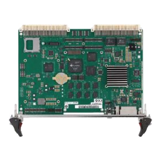
Page 31: Figure 1-1 Mvme2500-Ecc Ieee Board
Introduction Table 1-1 Key Features of the MVME2500-ECC (continued) Function Features Operating System Based from BSP provided by Freescale which is based from standard Linux version 2.6.32-rc3 Development tool is ltib 9.1.1 (Linux Target Image Builder) from Freescale VxWorks ... -
Page 32: Standard Compliances
The product is designed to meet the following standards. Results are pending until testing is finished. Table 1-2 Board Standard Compliances Standard Description EN 60950-1/A11:2009 Safety Requirements (legal) IEC 60950-1:2005 2nd Edition CAN/CSA C22.2 No 60950-1 MVME2500-ECC Installation and Use (6806800N30G) -
Page 33: Mechanical Data
233.44 mm (9.2 inches) Depth 160.0 mm (6.3 inches) Front Panel Height 261.8 mm (10.3 inches) Width 19.8 mm (0.8 inches) Max. Component Height 14.8 mm (0.58 inches) Weight 400 grams (standard variant), 700 grams (ET variants) MVME2500-ECC Installation and Use (6806800N30G) -
Page 34: Ordering Information
SERIAL-MINI-D2 SERIAL CABLE - MICRO D SUB CONNECTOR TO STANDARD DB9 MVME7216E-101 VME RTM (IEEE handle) MVME7216E-102 VME RTM (SCANBE Handle) MVME721ET-101 VME RTM Extended Temperature (IEEE handle) MVME721ET-102 VME RTM Extended Temperature (SCANBE Handle) MVME2500-ECC Installation and Use (6806800N30G) - Page 35 Female - to -male micro-mini DB-9 to DB9 adapter cable W2400E01A) Note: VME-HDMNTKIT can only be used with standard temp boards, MVME2500-01080101E, MVME2500-01080101S, MVME2500-02120201E and MVME2500-02120201S. VME-HDMNKIT2 can only be used with extended temp boards, MVME2500-02100202E and MVME2500-02100202S. MVME2500-ECC Installation and Use (6806800N30G)
-
Page 36: Product Identification
Introduction Product Identification The following graphics shows the location of the serial number label. Figure 1-3 Serial Number Location MVME2500-ECC Installation and Use (6806800N30G) -
Page 37: Hardware Preparation And Installation
This chapter provides installation and safety instructions for this product. Installation instructions for the optional PMC and transition module are also included. A fully implemented MVME2500-ECC consists of the base board plus: PCI Mezzanine Card (PMC) or PCI express Mezzanine Card (XMC) for added versatility ... -
Page 38: Unpacking And Inspecting The Board
The product is thoroughly inspected before shipment. If any damage occurred during transportation or any items are missing, contact customer service immediately. Requirements Make sure the board meets the requirements specified in the next sections when the board is operated in your particular system configuration. MVME2500-ECC Installation and Use (6806800N30G) -
Page 39: Environmental Requirements
0.04g2/Hz, 15 to 2000 Hz (8 (1hr/axis) GRMS) Shock 20g/11 mS 30g/11 mS Humidity to 95% RH (non-condensing) to 100% RH (non-condensing) 1. ft3/min minimum 2. Flat 15-1000Hz, -6db/octave 1000Hz - 2000Hz [MIL-STD 810F Figure 514.5C-17] MVME2500-ECC Installation and Use (6806800N30G) -
Page 40: Power Requirements
The board uses +5.0 V from the VMEbus backplane. On board power supply generates the required voltages for the various ICs. The MVME2500-ECC connects the +12 V and -12 V supplies from the backplane to the PMC sites, while the +3.3 V power supplied to the PMC sites comes from the +5.0 V backplane power. -
Page 41: Table 2-2 Power Requirements
The power is measured when the board is in standby (Linux prompt). Power will significantly increase when adding hard drives or a XMC/PMC card. The following table shows the power available when the MVME2500-ECC is installed in either a three row or five row chassis and when PMCs are present. -
Page 42: Equipment Requirements
Hardware Preparation and Installation 2.3.3 Equipment Requirements The following are recommended to complete a MVME2500-ECC system: VMEbus system enclosure System console terminal Operating system (and/or application software) Transition module and connecting cables Configuring the Board The board provides software control over most options. Settings can be modified to fit the user's specifications. -
Page 43: Installing Accessories
Installing Accessories 2.5.1 Rear Transition Module The MVME2500-ECC does not support hot swap. Remove power to the rear slot or system before installing the module. A PCMI/O Module (PIM) needs to be manually configured and installed before placing the transition module. -
Page 44: Pmc/Xmc Support
ESD-safe environment. Product Damage Inserting or removing modules with power applied may result in damage to module components. Before installing or removing additional devices or modules, read the documentation that came with the product. MVME2500-ECC Installation and Use (6806800N30G) -
Page 45: Installing And Removing The Board
This section describes the recommended procedure for installing the board in a chassis. Read all warnings and instructions before installing the board. The MVME2500-ECC does not support hot swap. Power off the slot or system and make sure that the serial ports and switches are properly configured. - Page 46 Connect the appropriate cables to the board. To remove the board from the chassis, reverse the procedure and press the red locking tabs (IEEE handles only) to extract the board. MVME2500-ECC Installation and Use (6806800N30G)
-
Page 47: Completing The Installation
Make sure the TPE bushing of the system is connected only to safety extra low voltage circuits (SELV circuits). If in doubt, ask your system administrator. The console settings for the MVME2500-ECC are: Eight bits per character One stop bit per character ... - Page 48 Hardware Preparation and Installation MVME2500-ECC Installation and Use (6806800N30G)
-
Page 49: Controls, Leds, And Connectors
Chapter 3 Controls, LEDs, and Connectors Board Layout The following figure shows the components and connectors on the MVME2500-ECC, applicable to both standard and extended variants. Figure 3-1 Component Layout MVME2500-ECC Installation and Use (6806800N30G) -
Page 50: Front Panel
Controls, LEDs, and Connectors Front Panel The following components are found on the MVME2500-ECC front panel, for both the standard and ET variants. Figure 3-2 Front Panel LEDs, Connectors and Switches MVME2500-ECC Installation and Use (6806800N30G) -
Page 51: Reset Switch
3.2.1 Reset Switch The MVME2500-ECC has a single push button switch that has both the abort and reset functions. Pressing the switch for less than three seconds generates an abort interrupt to the P20x0 QorIQ PIC. Holding it down for more than three seconds will generate a hard reset. The VME SYSRESET is generated if the MVME2500-ECC is the VMEbus system controller. - Page 52 GENET2 TSEC2 Front panel No link SPEED Link/Speed Integrated Amber 10/100BASE-T operation RJ45 LED Green 1000BASE-T operation (Left) GENET2 TSEC2 Front panel No activity Activity Integrated Blinking Green Activity proportional to bandwidth RJ45 LED utilization MVME2500-ECC Installation and Use (6806800N30G)
-
Page 53: Onboard Leds
This indicator is lit when the early 3.3V power supply fails. User Defined Amber Controlled by the FPGA User Defined Amber Controlled by the FPGA Connectors This section describes the pin assignments and signals for the connectors on the MVME2500- ECC. MVME2500-ECC Installation and Use (6806800N30G) -
Page 54: Front Panel Connectors
3.4.1 Front Panel Connectors The following connectors are found on the outside of the MVME2500-ECC. These connectors are divided between the front panel connectors and the backplane connectors. The front panel connectors include the J1 and J5 connectors. The backplane connectors include the P1 and P2 connectors. -
Page 55: Front Panel Serial Port (J4)
There is one front access asynchronous serial port interface that is routed to the micro mini DB- 9 front panel connector. A male-to-male micro-mini DB9 adapter cable is available under Artesyn part number SERIAL-MINI-D (30-W2400E01A). The pin assignments for these connectors are as follows:... -
Page 56: Usb Connector (J5)
Controls, LEDs, and Connectors 3.4.1.3 USB Connector (J5) The MVME2500-ECC uses upright USB receptacle mounted in the front panel. Table 3-5 USB Connector (J5) Pin Name Signal Description +5 V Data - Data + Mounting Ground Mounting Ground Mounting Ground Mounting Ground 3.4.1.4... - Page 57 IRQ5 ADD 34 +3.3V (not used) ADD 4 ADD 35 IRQ4 ADD 3 IRQ3 ADD 36 +3.3V (not used) ADD 2 IRQ2 ADD 37 ADD 1 IRQ1 ADD 38 +3.3V (not used) -12V +12V +12V MVME2500-ECC Installation and Use (6806800N30G)
-
Page 58: Vmebus P2 Connector
The VME P2 connector is a 160-pin DIN. Row B of the P2 connector provides power to the MVME2500-ECC and to the upper eight VMEbus address lines and additional 16 VMEbus data lines. The Z, A, C, and D pin assignments for the P2 connector are the same for both the... -
Page 59: Onboard Connectors
Onboard Connectors 3.4.2.1 Flash Program Connector (P7) The Flash Program Connector is depopulated in the production version of the MVME2500-ECC. However, each pin is exposed for the 60-pin header connector for the JTAG boundary scan. Table 3-8 Flash Programming Header (P7) -
Page 60: Sata Connector (J3)
Table 3-8 Flash Programming Header (P7) (continued) Signal Description Master OUT Slave IN (MOSI) 3.4.2.2 SATA Connector (J3) The onboard customized SATA connector is compatible with the Artesyn SATA kit, namely VME-64GBSSDKIT and IVME7210-MNTKIT. Table 3-9 Custom SATA Connector (J3) Signal Description Signal Description... -
Page 61: Pmc Connectors
+3.3V 3.4.2.3 PMC Connectors The MVME2500-ECC supports only one PMC site. It utilizes J14 to support PMC I/O that goes to the RTM PMC. The tables below show the pinout detail of J11, J12, J13 and J14. See Figure 3-1 for the location of the PMC connectors. - Page 62 AD 21 AD 1 AD 19 AD 0 +3.3V AD 17 REQ64 Table 3-11 PMC J12 Connector Signal Description Signal Description +12V JTAG TRST IDSELB JTAG TMS TRDY JTAG TDO +3.3V JTAG TDI STOP PERR +3.3V MVME2500-ECC Installation and Use (6806800N30G)
- Page 63 AD 7 AD 29 REQB +3.3V AD 26 GNTB AD 24 +3.3V IDSEL AD 23 EREADY +3.3V AD 28 RSTOUT AD 18 ACK64 +3.3V AD 16 CBE2 Table 3-12 PMC J13 Connector Signal Description Signal Description MVME2500-ECC Installation and Use (6806800N30G)
- Page 64 AD 40 AD 39 AD 60 AD 38 AD 59 AD 37 AD 58 AD 57 AD 36 +3.3V AD 35 AD 56 AD 34 AD 55 AD 33 AD 54 AD 53 +3.3V AD 32 MVME2500-ECC Installation and Use (6806800N30G)
- Page 65 PMC IO 15 PMC IO 47 PMC IO 16 PMC IO 48 PMC IO 17 PMC IO 49 PMC IO 18 PMC IO 50 PMC IO 19 PMC IO 51 PMC IO 20 PMC IO 52 MVME2500-ECC Installation and Use (6806800N30G)
-
Page 66: Jtag Connector (P6)
SPI HOLD 0 SPI CS 0 SPI CLK SPI CS 1 SPI HOLD 1 SPI MOSI SPI MISO SPI VCC SCAN 1 TCK SCAN 1 TDI SCAN 1 TRST SCAN 1 TDO SCAN 1 TMS +3.3V MVME2500-ECC Installation and Use (6806800N30G) - Page 67 SCAN 4 TDO SCAN 4 TCK 2 +3.3V SCAN 4 TDI SCAN 4 TCK 3 SCAN 4 TRST SCAN 5 TMS SCAN 5 SCAN 5 TDO +3.3V SCAN5 TCK2 SCAN 5 TDI SCAN 5 TRST MVME2500-ECC Installation and Use (6806800N30G)
-
Page 68: Cop Connector (P6)
COP VDD SENSE JTAG TCK COP CHECK STOP IN JTAG TMS P2020 SW RESET COP PRESENT COP HARD RESET KEYING COP CHECK STOP OUT 3.4.2.6 SD Connector (J2) Table 3-16 SD Connector (J2) Signal Description DATA 3 MVME2500-ECC Installation and Use (6806800N30G) -
Page 69: Xmc Connector (Xj2)
CARD DETECT 3.4.2.7 XMC Connector (XJ2) The MVME2500-ECC has one XMC connector (XJ2) that supports XMC cards with J15 connector. It can also support XMC cards with J16 connector without encountering any mechanical interference. Table 3-17 XMC Connector (XJ2) Pinout... -
Page 70: Miscellaneous P2020 Debug Connectors
GA 2 I2C DATA +3.3V MVMRO I2C CLOCK (PULLED DOWN) CLK + CLK - ROOT0 (PULLED UP) 3.4.2.8 Miscellaneous P2020 Debug Connectors Table 3-18 P20x0 Debug Header Signal Description MSRCDI0 MSRCDI1 MDVAL MSRCDI2 TRIG_OUT MSRCDI3 MVME2500-ECC Installation and Use (6806800N30G) -
Page 71: Switches
Table 3-18 P20x0 Debug Header (continued) Signal Description TRIG_IN MSRCID4 Switches These switches control the configuration of the MVME2500-ECC. Board Malfunction Switches marked as “reserved” might carry production-related functions and can cause the board to malfunction if their settings are changed. -
Page 72: Table 3-19 Geographical Address Switch
SCON mode which works in conjunction with the VME SCON SEL switch. 2. The VME SCON SEL switch is OFF to select non-SCON mode. The switch is ON to select always SCON mode. This switch is only effective when the VME SCON MAN switch is "ON". MVME2500-ECC Installation and Use (6806800N30G) -
Page 73: Smt Configuration Switch (S2)
FLASH_BOOT_BLOCK B = = switch is OFF switch is ON OFF (WP Disabled) WP_Disabled = switch is SPI Flash Write-Protect EEPROM_WP_Disabled = EEPROM_WP_Disabled = switch is OFF switch is ON OFF (133 MHz) PMC_133 PCI frequency selection MVME2500-ECC Installation and Use (6806800N30G) - Page 74 OFF (Front) GBE_MUX_SEL User Defined switch that will select if the GBE PHY will function on the front panel or on the Back PLANE OFF (CPU Reset Reserved Should be "OFF" for Deasserted) normal operation. MVME2500-ECC Installation and Use (6806800N30G)
-
Page 75: Functional Description
Figure 4-1 Block Diagram Chipset The MVME2500-ECC utilizes the QorIQ P20x0 integrated processor. It offers an excellent combination of protocol and interface support including dual high performance CPU cores, a large L2 cache, a DDR2/DDR3 memory controller, three enhanced three-speed Ethernet controllers, two Serial RapidIO interfaces with a messaging unit, a secure digital interface, a USB 2.0 interface and three PCI express controllers. -
Page 76: E500 Processor Core
Functional Description This section describes the protocol and interfaces provided in the QorIQ P20x0 integrated and is utilized by the MVME2500-ECC. 4.2.1 e500 Processor Core The QorIQ integrated processors offer dual high performance e500v2 core (P2020) and a single e500v2 core (P2010). It operates from 800 MHz up to 1.2GHz core frequency. The e500... -
Page 77: Pci Express Interface
MMC and SD. It is compatible with the SD Host Controller Standard Specification Ver. 2.0 and supports the following: SD, miniSD, SD Combo, MMC+ and RS-MMC card. 4.2.6 C Interface The MVME2500-ECC uses only one of the two independent I C buses on the processor. For more information, see I2C Devices, on page 4.2.7... -
Page 78: Duart
The eTSEC controller of the device communicates to the 10 Mbps, 100 Mbps, and 1 Gbps Ethernet/IEE 802.3 networks, as well as to devices with generic 8 to 16-bit FIFO ports. The MVME2500-ECC uses the eTSEC using the RGMII interface. 4.2.11 General Purpose I/O (GPIO) The P20x0 has a total of sixteen I/O ports. -
Page 79: Common On-Chip Processor (Cop)
2GB of ECC memory using 2 Gbit (256M x8) device densities. The MVME2500-ECC has a total of six board variants; four of which are commercial temperature and have both 2GB and 1GB of memory, whereas the other two variants are Extended Temperature (ET) and have 2GB of memory. -
Page 80: Internal Timer
FPGA to provide fully programmable registers for the timers. Ethernet Interfaces The MVME2500-ECC has three eTSEC controllers. Each one supports RGII, GMII, and SGMII interface to the external PHY. All controllers can only be utilized when using the RGMII interface. Using the GMII allows only up to two usable controllers. -
Page 81: Spi Bus Interface
4.6.1 SPI Flash Memory The MVME2500-ECC has two 8 MB onboard serial flash. Both contain the ENV variables and the U-Boot firmware image, which is about 513 KB in size. Both SPI flash contain the same programming for firmware redundancy and crisis recovery. The SPI flash can be programmed through the JTAG interface or through an onboard SPI flash programming header. -
Page 82: Firmware Redundancy
4.6.3 Firmware Redundancy The MVME2500-ECC uses two physically separate boot devices to provide boot firmware redundancy. Although the P20x0 provides four SPI Bus chip-selects, the P20x0 is only capable of booting from the SPI Device controlled by Chip Select 0. External SPI multiplexing logic is implemented on the MVME2500-ECC to accommodate this chipset limitation. -
Page 83: Figure 4-2 Spi Device Multiplexing Logic
Functional Description The MVME2500-ECC FPGA controls the chip select to SPI devices A and B. The FPGA chip select control is based on the Switch Bank (S2-2). Figure 4-2 SPI Device Multiplexing Logic At power-up, the selection of the SPI boot device is strictly based upon the Switch Bank (S2-2) setting. -
Page 84: Crisis Recovery
Functional Description The MVME2500-ECC supports automatic switch over. If booting one device is not successful, the watchdog will trigger the board reset and it will automatically boot on the other device. 4.6.4 Crisis Recovery The MVME2500-ECC provides an independent boot firmware recovery mechanism for the operating system. -
Page 85: Front Uart Control
MVME2500-ECC. PMC/XMC Sites The MVME2500-ECC hosts only one PMC/XMC site and accepts either a PMC or an XMC add-on card. Only an XMC or a PMC may be populated at any given time as both occupy the same physical space on the PCB. -
Page 86: Pmc Add-On Card
PMC/XMC sites are keyed for 3.3V PMC signaling. PMC and XMC add-on cards must have a hole in the 3.3 V PMC keying position in order to be populated on the MVME2500-ECC. The XMC specification accommodates this since it is expected that carrier cards will host both XMC and PMC capable add-on cards. -
Page 87: Sata Interface
4.11.1 Tsi148 VME Controller The VMEbus interface for the MVME2500-ECC is provided by the Tsi148 VMEbus controller. The Tsi148 provides the required VME, VME extensions, and 2eSST functions. TI SN74VMEH22501transceivers are used to buffer the VME signals between the Tsi148 and the VME backplane. -
Page 88: I2C Devices
4.13 I C Devices The MVME2500-ECC utilizes one of the two I2C ports provided by the board's processor. The C bus is a two-wire, serial data (SDA) and serial clock (SCL), synchronous, multi-master bi- directional serial bus that allows data exchange between this device and other devices such as VPD, SPD, EEPROM, RTC, temperature sensor, RTM, XMC and IDT clocking. -
Page 89: Onboard Voltage Supply Requirement
1.26 V +1.05 V 1.0 V 1.1 V 4.15.2 Power Up Sequencing Requirements The power up sequence describes the voltage rail power up timing, which is designed to support all the chip supply voltage sequencing requirement. MVME2500-ECC Installation and Use (6806800N30G) -
Page 90: Clock Structure
Clock Distribution Diagram 4.17 Reset Structure MVME2500-ECC reset will initiate after the power up sequence if the 1.5 V power supply is "GOOD". When the board is at "ready" state, the reset logic will monitor the reset sources and implement the necessary reset function. -
Page 91: Reset Sequence
4.18 Thermal Management The MVME2500-ECC utilizes two on-board temperature sensors: one for the board and the other for the CPU temperature sensor. The board temperature sensor is located near the dual RJ45 connector near the front panel. The CPU temperature sensor is located near the P2020 CPU. -
Page 92: Real-Time Clock Battery
In this case, the Renata battery specification is better than the BR type. The battery type used on the ENP2 board is the CR2325 from Renata. 4.20 Debugging Support The following information shows the details of Artesyn debugging support as applied to the MVME2500-ECC. 4.20.1 POST Code Indicator The following table shows the LED status of the POST Codes. -
Page 93: Custom Debugging
4.20.2 Custom Debugging Custom debugging makes use of the common on-chip processor. Refer to Common On-Chip Processor (COP), on page 79 for details. 4.21 Rear Transition Module (RTM) The MVME2500-ECC is compatible with the MVME721x RTM. MVME2500-ECC Installation and Use (6806800N30G) -
Page 94: Table 4-5 Transition Module Features
The MVME721X RTM is for I/O routing through the rear of a compact VMEbus chassis. It connects directly to the VME backplane in chassis with an 80 mm deep rear transition area. The MVME721X RTM is designed for use with the MVME7100, MVME2500-ECC, MVME2500ET- ECC, iVME7210, and MVME 4100. It has the following features:... -
Page 95: Memory Maps And Registers
Memory Maps and Registers Overview System resources including system control and status registers, external timers, and the QUART are mapped into 16 MB address range accessible from the MVME2500-ECC local bus through the P20x0 Q or IQ LBC. Memory Map The following table shows the physical address map of the MVME2500-ECC. -
Page 96: Linux Devices Memory Map
I2C2 CCSR 0xffe03100 0xffe031ff 256 B UART0 CCSR 0xffe04500 0xffe045ff 256 B UART1CCSR 0xffe04600 0xffe046ff 256 B ELBC CCSR 0xffe05000 0xffe05fff 4 KB SPI CCSR 0xffe07000 0xffe07fff 4 KB PCIE3 CCSR 0xffe08000 0xffe08fff 4 KB MVME2500-ECC Installation and Use (6806800N30G) -
Page 97: Programmable Logic Device (Pld) Registers
Programmable Logic Device (PLD) Registers 5.4.1 PLD Revision Register The MVME2500-ECC provides a PLD revision register that can be read by the system software to determine the current version of the timers/registers PLD. Table 5-3 PLD Revision Register PLD Revision Register - 0xFFDF0000... -
Page 98: Pld Year Register
8-bit field containing the current timer/register PLD revision. The revision number starts at 01. 5.4.2 PLD Year Register The MVME2500-ECC PLD provides an 8-bit register which contains the build year of the timers/registers PLD. Table 5-4 PLD Year Register PLD Year Register - 0xFFDF0004... -
Page 99: Pld Day Register
PLD Rev OPER RESET 5.4.5 PLD Sequence Register The MVME2500-ECC PLD provides an 8-bit register which contains the sequence of the PLD which is in synchrony with the PCB version. Table 5-7 PLD Sequence Register PLD Revision Register - 0xFFDF0007 Field... -
Page 100: Pld Power Good Monitor Register
Memory Maps and Registers 5.4.6 PLD Power Good Monitor Register The MVME2500-ECC PLD provides an 8-bit register which indicates the instantaneous status of the supply’s power good signals. Table 5-8 PLD Power Good Monitor Register PLD PWRDG_MNTR - 0xFFDF0012 Field... -
Page 101: Pld Led Control Register
Table "Front Panel LEDs" on page 52 Table "Onboard LEDs Status" on page 5.4.8 PLD PCI/PMC/XMC Monitor Register The MVME2500-ECC PLD provides an 8-bit register which indicates the status of the PCI/PMC/XMC interface signals. Table 5-10 PLD PCI/PMC/XMC Monitor Register PLD PCI_PMC_XMC_MNTR - 0xFFDF001D Field... -
Page 102: Pld U-Boot And Tsi Monitor Register
0 - PCI capable 5.4.9 PLD U-Boot and TSI Monitor Register The MVME2500-ECC PLD provides an 8-bit register which indicates the status of the U-Boot's normal environment switch and TSI interface signals. Table 5-11 PLD U-Boot and TSI Monitor Register... -
Page 103: Pld Boot Bank Register
0 - Non-system Controller 5.4.10 PLD Boot Bank Register The MVME2500-ECC PLD provides an 8-bit register which is used to declare successful U-Boot loading, indicating the SPI boot bank priority and actual SPI bank it booted from. Table 5-12 PLD Boot Bank Register... - Page 104 Board automatically switches-to and successfully boots-from the good SPI Flash 1 User replaces the image in SPI Flash 0 with a new good one User power-cycles the blade in order to ensure continued accuracy of BOOT_SPI MVME2500-ECC Installation and Use (6806800N30G)
-
Page 105: Pld Write Protect And I2C Debug Register
Memory Maps and Registers 5.4.11 PLD Write Protect and I2C Debug Register The MVME2500-ECC PLD provides an 8-bit register which is used to indicate the status of I2C and SPI write-protect manual switches and is used to control the SPI write-enable. I2C debug ports are also provided in this register which can be used in controlling the bus’... - Page 106 I2C debug port-Clock I2C_DEBUG_EN=0 HiZ - Tri-Stated I2C_DEBUG_EN-1 1 - Driven High 0 - Driven Low When SERIAL_FLASH_WP is set to "Low", this port will automatically read as low due to "AND" connection between the two ports. MVME2500-ECC Installation and Use (6806800N30G)
-
Page 107: Pld Test Register 1
Memory Maps and Registers 5.4.12 PLD Test Register 1 The MVME2500-ECC PLD provides an 8-bit general purpose read/write register which can be used by the software for PLD testing or general status bit storage. Table 5-14 PLD Test Register 1... -
Page 108: Pld Gpio2 Interrupt Register
Memory Maps and Registers 5.4.14 PLD GPIO2 Interrupt Register The Abort switch, Tick Timer 0, 1 and 2 interrupts are ORed together. The MVME2500-ECC provides an interrupt register that the system software reads to determine which device the interrupt originated from. GPIO2 will be driven "low" if any of the interrupts asserts. -
Page 109: Reset Control And Reset Reason Register
Memory Maps and Registers 5.4.15 Reset Control and Reset Reason Register The MVME2500-ECC provides an 8-bit register to execute the shutdown and reset commands. The board's reset reason is also included in this register. Table 5-17 PLD Shutdown and Reset Control and Reset Reason Register... -
Page 110: Pld Watchdog Timer Refresh Register
0 - None 5.4.16 PLD Watchdog Timer Refresh Register The MVME2500-ECC provides a watchdog timer refresh register. Table 5-18 PLD Watchdog Timer Refresh Register PLD Watch Dog Timer Load - 0xFFC80600 7 6 5 4 3 2 1 0... -
Page 111: Pld Watchdog Control Register
Enable. If cleared, the watchdog timer is disabled. If set, the watchdog timer is enabled. 5.4.18 PLD Watchdog Timer Count Register The MVME2500-ECC provides a watchdog timer count register. Table 5-20 PLD Watchdog Timer Count Register PLD Watchdog Timer Count - 0xffc80606... -
Page 112: External Timer Registers
60 seconds. External Timer Registers The MVME2500-ECC provides a set of tick timer registers to access the three external timers implemented in the timers/registers PLD. These registers are 32-bit and are word writable. The following sections describe the timer prescaler and control registers. -
Page 113: Control Registers
1 to the COVF bit. ENINT Enable Interrupt. When the bit is set, the interrupt is enabled. When the bit is cleared, the interrupt is not enabled. CINT Clear Interrupt. INTS Interrupt Status. RSVD Reserved for future implementation. MVME2500-ECC Installation and Use (6806800N30G) -
Page 114: Compare High And Low Word Registers
Tick Timer 0 Compare Value Low Word - 0xFFC80206 Tick Timer 1 Compare Value Low Word - 0xFFC80306 Tick Timer 2 Compare Value Low Word - 0xFFC80406 Field TickTimer Compare Value Low Word (16-bits) OPER RESET 0x0000 MVME2500-ECC Installation and Use (6806800N30G) -
Page 115: Counter High And Low Word Registers
Tick Timer 0 Counter Value Low Word - 0xFFC8020A Tick Timer 1 Counter Value Low Word - 0xFFC8030A Tick Timer 2 Counter Value Low Word - 0xFFC8040A Field TickTimer Counter Value Low Word (16-bits) OPER RESET 0x0000 MVME2500-ECC Installation and Use (6806800N30G) - Page 116 Memory Maps and Registers MVME2500-ECC Installation and Use (6806800N30G)
-
Page 117: Boot System
Chapter 6 Boot System Overview The MVME2500-ECC uses Das U-Boot, a boot loader software based on the GNU Public License. It boots the blade and is the first software to be executed after the system is powered Its main functions are: Initialize the hardware ... -
Page 118: Boot Options
TFTP server. Configure U-Boot environment variables: setenv ipaddr <IP address of MVME2500-ECC> setenv serverip <IP address of TFTP server> setenv gatewayip <gateway IP> setenv netmask <netmask> setenv bootargs 'root=/dev/ram rw console=ttyS0,9600n8... -
Page 119: Booting From An Optional Sata Drive
# option: usb - interface, 0:1 - device 0 partition 1 fatload usb 0:1 1000000 $File_uImage fatload usb 0:1 2000000 $File_ramdisk fatload usb 0:1 c00000 $File_dtb 5. Boot the Linux in memory: bootm 1000000 2000000 c00000 MVME2500-ECC Installation and Use (6806800N30G) -
Page 120: Booting From An Sd Card
In this mode, the U-Boot downloads and boots VxWorks from an external TFTP server. Make sure that the VxWorks image is accessible by the board from the TFTP server. 2. Configure U-Boot environment variables: setenv ipaddr <IP address of MVME2500-ECC> setenv serverip <IP address of TFTP server> setenv gatewayip <gateway IP>... -
Page 121: Using The Persistent Memory Feature
U-Boot reports less memory to the Linux kernel through the mem parameter, indicating that the operating system should not use it either. For more information, see the U-Boot documentation. MVME2500-ECC Installation and Use (6806800N30G) -
Page 122: Mvme2500-Ecc Specific U-Boot Commands
Boot System MVME2500-ECC Specific U-Boot Commands Table 6-1 MVME2500-ECC Specific U-Boot Commands Command Description base Print or set address offset bdinfo Print board info structure boot Boot default, i.e., run 'bootcmd' bootd Boot default, i.e., run 'bootcmd' bootelf Boot from an ELF image in memory... - Page 123 Boot System Table 6-1 MVME2500-ECC Specific U-Boot Commands (continued) Command Description help Print online help I2C sub-system iminfo Print header information for application image imxtract Extract a part of a multi-image interrupts Enable or disable interrupts itest Return true/false on integer compare...
-
Page 124: Updating U-Boot
Boot System Table 6-1 MVME2500-ECC Specific U-Boot Commands (continued) Command Description Run commands in an environment variable saveenv Save environment variables to persistent storage script Run a ';' delimited, ';;' terminated list of commands scsi SCSI sub-system scsiboot Boot from SCSI device... - Page 125 5. Write 0x90000 bytes from RAM address 0x1000000 starting at SPI address 0: sf write 0x1000000 0 0x90000 To replace the image in SPI bank 1, replace step 2 with Select SPI flash # 1: sf probe 1 MVME2500-ECC Installation and Use (6806800N30G)
- Page 126 Boot System MVME2500-ECC Installation and Use (6806800N30G)
-
Page 127: Programming Model
Overview This chapter includes additional programming information for the MVME2500-ECC. Reset Configuration The MVME2500-ECC supports the power-on reset (POR) pin sampling method for processor reset configuration. Each option and the corresponding default setting are described in the following table. Table 7-1 POR Configuration Settings... - Page 128 DDR Controller LA26 CFG_DDR_SPEED:1=DDR Speed FREQ>= 500 MHz Engineering use LA[22:20] 111111 Default (for future use) UART_SOUT[0], TRIG_OUT, MSRCID[1], MSRCID[4], DMA1_DDONE_B[0] SerDes Ref TSEC_1588_ALARM SerDes expects a 100 Clock Config _OUT1 MHz reference clock frequency (default). MVME2500-ECC Installation and Use (6806800N30G)
- Page 129 (or RGMII, if configured in reduced mode) if its not configured to operate in SGMII mode. ETSEC3 UART_RTS0, The eTSEC3 controller Protocol UART_RTS1 operates using the RGMII protocol if not configured to operate in SGMII mode. MVME2500-ECC Installation and Use (6806800N30G)
- Page 130 The power-on- reset sequence waits indefinitely for the SerDes PLL to lock (default). System Speed LA[28] SYSCLOCK is above 66 SDHC Card TSEC2_TXD_5 Not Inverted Detect Polarity RAPID System Default RapidIO is not used Size MVME2500-ECC Installation and Use (6806800N30G)
-
Page 131: Interrupt Controller
Programming Model Interrupt Controller The MVME2500-ECC uses the MPC8548E integrated programmable interrupt controller (PIC) to manage locally generated interrupts. Currently defined external interrupting devices and interrupt assignments, along with corresponding edge/levels and polarities, are shown in the following table. Table 7-2 MVME2500-ECC Interrupt List... -
Page 132: I2C Bus Device Addressing
Programming Model I2C Bus Device Addressing The following table contains the I2C devices used for the MVME2500-ECC and its assigned device address. Table 7-3 I2C Bus Device Addressing I2C Bus Address Device Function Size Notes 0x50 256 x 8 0x4C... -
Page 133: Other Software Considerations
7.6.3 Quad UART The MVME2500-ECC console RS232 port is driven by the UART built into the P20x0 QorIQ chip. Additionally, the MVME2500-ECC has a Quad UART chip which provides four additional 16550 compatible UART. These additional UART are internally accessed through the LBC bus. The Quad UART chip clock input (which is internally divided to generate the baud rate) is 1.8432... -
Page 134: Lbc Timing Parameters
10 - LCSn is outputted one quarter bus clock cycle after the address lines. XACS Extra Address to chip-select setup 0 - Address to chip-select setup is determined by ORx[ACS] Cycle length in bus clocks 0011 - Three bus clock cycle wait state MVME2500-ECC Installation and Use (6806800N30G) -
Page 135: Clock Distribution
Ethernet PHY and SATA bridge are supplied by ICS83905. Most of the QorIQ P2020 clocks are generated by ICS840S07I chip. Additional clocks required by individual devices are generated near the devices using individual oscillators. The following table lists the clocks required on the MVME2500-ECC along with the frequency and source. Table 7-6 Clock Distribution Device... -
Page 136: System Clock
System Clock The system and DDR clock is driven by ICS840S07I. The following table defines the clock frequency. Table 7-7 System Clock SYSCLK CORE CCB Clock (Platform) DDR3 100MHz 800/1200 MHz 400 MHz 400MHz 25MHz MVME2500-ECC Installation and Use (6806800N30G) -
Page 137: Real Time Clock Input
7.7.3 Local Bus Controller Clock Divisor The local bus controller (LBC) clock output is connected to the FPGA for LBC bus transaction. It is also the source of 1 MHz (CPU_RTC) and FPGA tick timers. MVME2500-ECC Installation and Use (6806800N30G) - Page 138 Programming Model MVME2500-ECC Installation and Use (6806800N30G)
-
Page 139: Replacing The Battery
Replacing the Battery Replacing the Battery The figure below shows the location of the board battery. This section applies only to the MVME2500-ECC commercial temperature board. The MVME2500ET-ECC does not have a battery to be replaced. Figure A-1 Battery Location... - Page 140 The battery provides seven years of data retention, summing up all periods of actual data use. Artesyn Embedded Technologies therefore assumes that there is usually no need to replace the battery except, for example, in case of long-term spare part handling.
- Page 141 To replace the battery, proceed as follows: 1. Remove the old battery. 2. Install the new battery with the plus sign (+) facing up. Dispose of the old battery according to your country’s legislation and in an environmentally safe way. MVME2500-ECC Installation and Use (6806800N30G)
- Page 142 Replacing the Battery MVME2500-ECC Installation and Use (6806800N30G)
-
Page 143: Related Documentation
The publications listed below are referenced in this manual. You can obtain electronic copies of Artesyn Embedded Technologies - Embedded Computing publications by contacting your local Artesyn sales office. For released products, you can also visit our Web site for the latest copies of our product documentation. -
Page 144: Related Specifications
PCI Local Bus Specification PCI Rev 3.0 Interest Group PCI-X Electrical and Mechanical Addendum to the PCI Local Bus (PCI-SIG) Specification (PCI-X EM) Revision 2.0a PCI-X Protocol Addendum to the PCI Local Bus Specification (PCI-X PT) Revision 2.0a MVME2500-ECC Installation and Use (6806800N30G) - Page 145 Serial ATA II: Extensions to Serial ATA 1.0 Revision 1.0 (SATA-IO) Trusted Computing TPM Specification 1.2, Level 2 Revision 103 Version 1.2 Group (TCG) USB Implementers Universal Serial Bus Specification (USB) Revision 2.0 Forum (USB-IF) MVME2500-ECC Installation and Use (6806800N30G)
- Page 146 Related Documentation MVME2500-ECC Installation and Use (6806800N30G)
- Page 148 Artesyn Embedded Technologies, Artesyn and the Artesyn Embedded Technologies logo are trademarks and service marks of Artesyn Embedded Technologies, Inc. All other product or service names are the property of their respective owners. © 2016 Artesyn Embedded Technologies, Inc.
Need help?
Do you have a question about the MVME2500-ECC and is the answer not in the manual?
Questions and answers