Table of Contents
Advertisement
Quick Links
Advertisement
Table of Contents

Related Manuals for Artesyn MVME8100


Summary of Contents for Artesyn MVME8100
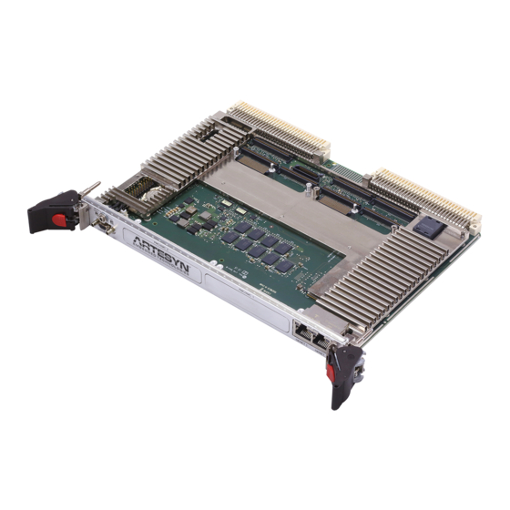
- Page 1 MVME8100/MVME8105/MVME8110 Installation and Use P/N: 6806800P25N April 2019...
- Page 2 Artesyn reserves the right to revise this document and to make changes from time to time in the content hereof without obligation of Artesyn to notify any person of such revision or changes.
-
Page 3: Table Of Contents
Front Panel ............... . 53 MVME8100/MVME8105/MVME8110 Installation and Use (6806800P25N) - Page 4 4.11 Rear UART Ports ..............89 MVME8100/MVME8105/MVME8110 Installation and Use (6806800P25N)
- Page 5 5.3.5 Booting VxWorks through the Network ........107 MVME8100/MVME8105/MVME8110 Specific U-Boot Commands ..... . . 107 Updating U-Boot .
- Page 6 Artesyn Embedded Technologies Documentation ........
- Page 7 MVME8100 - ENP4 LEDs and Switches ........
- Page 8 List of Figures MVME8100/MVME8105/MVME8110 Installation and Use (6806800P25N)
- Page 9 VXS P0 Connector (applicable to MVME8100 only) ....... . .
- Page 10 List of Tables MVME8100/MVME8105/MVME8110 Installation and Use (6806800P25N)
-
Page 11: About This Manual
About this Manual Overview of Contents This manual provides the information required to install and configure the Artesyn MVME8100, MVME8105 and MVME8110 boards. Additionally, this manual provides specific preparation and installation information and data applicable to the board. The MVME8100 and MVME8105 are high-performance, dual core processor boards featuring ©... - Page 12 Institute of Electrical and Electronics Engineers Inter IC Initial Hardware Watchdog JTAG Joint Test Access Group Local Bus Controller MRAM Magnetoresistive random-access memory OSWD OS Watchdog PCIE Peripheral Component Interconnect Express PCI-X Peripheral Component Interconnect -X Programmable Interrupt Controller MVME8100/MVME8105/MVME8110 Installation and Use (6806800P25N)
- Page 13 Static Random Access Memory SRIO Serial Rapid IO TSEC Three-Speed Ethernet Controller 2eSST Two edge Source Synchronous Transfer UART Universal Asynchronous Receiver/Transmitter VITA VMEbus International Trade Association VMEbus (Versa Module Eurocard) Vital Product Data PCI Express Mezzanine Card MVME8100/MVME8105/MVME8110 Installation and Use (6806800P25N)
- Page 14 Ranges, for example: 0..4 means one of the integers 0,1,2,3, and 4 (used in registers) Logical OR Indicates a hazardous situation which, if not avoided, could result in death or serious injury. Indicates a hazardous situation which, if not avoided, may result in minor or moderate injury. MVME8100/MVME8105/MVME8110 Installation and Use (6806800P25N)
- Page 15 Updated Standard Compliances table. Added a notice under Table 2-3 on page 45 and updated 6806800P25M July 2016 Table 1-1 on page 37. Removed Declaration of Conformity of MVME8100, 6806800P25L May 2016 Declaration of Conformity of MVME8105, and Declaration of Conformity of MVME8110.
- Page 16 Figure 2-4 on page 53, Figure 3-2 on page 60, Interrupt Controller Assignments on page 105 and GPIO Electrical Characteristics on page 106. 6806800P25C December 2012 Updated Standard Compliances on page 34. 6806800P25B November 2012 GA release. 6806800P25A May 2012 First edition. MVME8100/MVME8105/MVME8110 Installation and Use (6806800P25N)
-
Page 17: Safety Notes
Failure to comply with these precautions or with specific warnings elsewhere in this manual could result in personal injury or damage to the equipment. Artesyn Embedded Technologies intends to provide all necessary information to install and handle the product in this manual. Because of the complexity of this product and its various uses, we do not guarantee that the given information is complete. - Page 18 Changes or modifications not expressly approved by Artesyn Embedded Technologies could void the user's authority to operate the equipment. Board products are tested in a representative system to show compliance with the above mentioned requirements.
- Page 19 Verify that the length of an electric cable connected to a TPE bushing does not exceed 100 meters. Make sure the TPE bushing of the system is connected only to safety extra low voltage circuits (SELV circuits). If in doubt, ask your system administrator. MVME8100/MVME8105/MVME8110 Installation and Use (6806800P25N)
- Page 20 When exchanging the on-board lithium battery, make sure that the new and the old battery are exactly the same battery models. If the respective battery model is not available, contact your local Artesyn Embedded Technologies sales representative for the availability of alternative, officially approved battery models.
-
Page 21: Sicherheitshinweise
Installieren Sie keine Ersatzteile oder führen Sie keine unerlaubten Veränderungen am Produkt durch, sonst verfällt die Garantie. Wenden Sie sich für Wartung oder Reparatur bitte an die für Sie zuständige Geschäftsstelle von Artesyn Embedded Technologies. So stellen Sie sicher, dass alle sicherheitsrelevanten Aspekte beachtet werden. - Page 22 Sicherheitshinweise Das Produkt wurde in einem Artesyn Embedded Technologies Standardsystem getestet. Es erfüllt die für digitale Geräte der Klasse A gültigen Grenzwerte in einem solchen System gemäß den FCC-Richtlinien Abschnitt 15 bzw. EN 55022 Klasse A. Diese Grenzwerte sollen einen angemessenen Schutz vor Störstrahlung beim Betrieb des Produktes in Gewerbe- sowie...
- Page 23 Sie, dass das Face Plate oder die Platine deformiert oder zerstört wird. Beschädigung des Produktes und von Zusatzmodulen Fehlerhafte Installation von Zusatzmodulen, kann zur Beschädigung des Produktes und der Zusatzmodule führen. Lesen Sie daher vor der Installation von Zusatzmodulen die zugehörige Dokumentation. MVME8100/MVME8105/MVME8110 Installation and Use (6806800P25N)
- Page 24 Wenn Sie die Batterie schnell austauschen, bleiben die Zeiteinstellungen möglicherweise erhalten. Datenverlust Wenn die Batterie wenig oder unzureichend mit Spannung versorgt wird, wird der RTC initialisiert. Tauschen Sie die Batterie aus, bevor sieben Jahre tatsächlicher Nutzung vergangen sind. MVME8100/MVME8105/MVME8110 Installation and Use (6806800P25N)
- Page 25 Um Schäden zu vermeiden, sollten Sie keinen Schraubendreher zum Ausbau der Batterie verwenden. Umweltschutz Unsachgemäße Entsorgung von gebrauchten Produkten kann die Umwelt schädigen. Entsorgen Sie gebrauchte Produkte stets gemäß der in Ihrem Land gültigen Gesetzgebung und den Empfehlungen des Herstellers. MVME8100/MVME8105/MVME8110 Installation and Use (6806800P25N)
- Page 26 Sicherheitshinweise MVME8100/MVME8105/MVME8110 Installation and Use (6806800P25N)
-
Page 27: Introduction
QorIQ P5020 processor. It runs at 2.0GHz with 4GB DDR3. The MVME8105 provides a second 1000Base-TX RJ-45 interface on the front panel. The MVME8110 is a single core non-VXS version of the MVME8100 board based on the NXP QorIQ P5010 processor. It runs at 1.2GHz with 2GB DDR3. -
Page 28: Feature Summary
High-speed USB 2.0 controllers with integrated PHYs CoreNet platform cache with ECC 2Mbyte 2Mbyte 1Mbyte SATA 2.0 controller RAID5/6 engine SEC encryption System Memory DDR3 SDRAM with ECC DDR3 data rate 1333MT/s 1333MT/s 1200MT/s SMBus MVME8100/MVME8105/MVME8110 Installation and Use (6806800P25N) -
Page 29: Table
USB 2.0 for backplane RTM I/O Ethernet 10/100/1000BASE-T Ethernet port to front panel 10/100/1000BASE-T Ethernet channels to P2/RTM 1000BASE-BX Ethernet SERDES channels to P0 backplane/RTM SATA Ports SATA Gen 3 ports to P0 backplane/RTM Serial Ports MVME8100/MVME8105/MVME8110 Installation and Use (6806800P25N) - Page 30 Front panel RJ-45 connector with integrated LEDs for 10/100/1000 Ethernet channel PMC/XMC Site 1 front I/O and rear PMC I/O PMC/XMC Site 2 front I/O Serial ports to P2/RTM, (two Micro DB-9 connectors on RTM panel and two on planar headers) MVME8100/MVME8105/MVME8110 Installation and Use (6806800P25N)
-
Page 31: Ordering And Support Information
ENP4 (conduction cooled) variant are accessed through P2 only. Ordering and Support Information The data sheets for the MVME8100, MVME8105 and MVME8110 boards contain a complete list of available variants and accessories. Refer to Appendix B Related Documentation or consult your local Artesyn sales representative for the availability of product variants. -
Page 32: Standard Compliances
Customers may still purchase the non-RoHS product (with a waiver) for use in applications excluded from RoHS compliance. Mechanical Data The MVME8100 is a full 6U board with added mounting holes to support an ENP4 board variant. The MVME8100/MVME8105/MVME8110 occupies a single VME card slot. -
Page 33: Mechanical Data
Table 1-3 Mechanical Data Characteristic Value Height 233.44mm (9.2 inches) Depth 160.0mm (6.3 inches) Front Panel Height 261.8mm (10.3 inches) Width 19.8mm (0.8 inches) Maximum Component Height 14.8mm (0.58 inches) 0.58Kg (ENP1) Weight (estimated) 0.90Kg (ENP4) MVME8100/MVME8105/MVME8110 Installation and Use (6806800P25N) - Page 34 Introduction Introduction NOTES MVME8100/MVME8105/MVME8110 Installation and Use (6806800P25N)
-
Page 35: Hardware Preparation And Installation
RTM. Configuring the Board on page 41 3. Install the MVME8100 RTM (VXS1-RTM1) or the MVME8110 RTM (MVME8110-RTM) in the chassis. Rear Transition Module on page 4. Install PMC module (if required). -
Page 36: Unpacking And Inspecting The Board
Hardware Preparation and Installation Hardware Preparation and Installation 10. Program the board as needed for your applications. MVME8100/MVME8105/MVME8110 Single Board Computer Programmer’s Reference. Unpacking and Inspecting the Board Read all notices and cautions prior to unpacking the product. NOTICE... -
Page 37: Requirements
MVME8100/MVME8105/MVME8110 baseboard appears in Chapter 4 Functional Description. The MVME8100 has ENP1 and ENP4 variants which comply with the following environmental and regulatory specifications. The MVME8105 has ENP1variant only which comply with the following environmental and regulatory specifications. - Page 38 Note: The MVME8100 ENP 4 version includes NAND Flash memory in the form of the eMMC. The specified storage limits for the MVME8100 ENP 4 version are -55°C to +105°C. It should be noted that the industry standard (for Flash) as well as the Storage Temperature -40°...
-
Page 39: Power Requirements
The MVME8100-202180404 is non-compliant with the EU RoHS Directive and the CE mark as of July 21, 2016. The following table shows the power limits due to the available 5 volts pins, when the MVME8100/MVME8105 is installed in either a 3-row or 5-row chassis and when PMCs/XMCs are present. Chassis Type... -
Page 40: Thermal Requirements
C sensor at address 0x4C on the processor I C bus #1. For more information, refer MVME8100/MVME8105/MVME8110 Single Board Computer Programmer's Reference. 2.3.5 Equipment Requirements The following equipment is recommended to complete a system using an MVME8100, MVME8105 or MVME8110 board: VMEbus system enclosure System console terminal ... -
Page 41: Configuring The Board
Make sure that all user-defined switches are properly set before installing a PMC/XMC module. For more information about switches, see Switches on page Prior to installing PMC modules on the MVME8100/MVME8105/MVME8110 baseboard, ensure that all switches that are user configurable are set properly. Refer to Figure 2-1... -
Page 42: Figure 2-2 Switch Locations (Enp4 Board)
Hardware Preparation and Installation Hardware Preparation and Installation Figure 2-2 Switch Locations (ENP4 Board) S4 Switch S5 Switch S3 Switch S2 Switch MVME8100/MVME8105/MVME8110 Installation and Use (6806800P25N) -
Page 43: Installing Accessories
2.5.1 Rear Transition Module The RTM of MVME8100/MVME8105/MVME8110 does not support hot swap. You must remove power to the system before installing the module. Before installing the transition module, you may need to manually configure the RTM switches and install a PMC I/O Module (PIM). -
Page 44: Pmc/Xmc Installation
+3.3V I/O PMC modules. The on-board PMC sites do not support +5.0V I/O PMC modules. The MVME8100 ENP4 version only supports rugged conduction cooled PMC/XMC modules (see VITA 20-2001 for conduction cooled PMC for mechanical definition. - Page 45 Hardware Preparation and Installation Follow the steps to install a PMC/XMC module onto the MVME8100/MVME8105/MVME8110 board. Installation Procedure Read all notices and follow the steps to install a PMC/XMC on the baseboard. NOTICE Logic Ground to Chassis Ground Isolation The MVME8100/MVME8105/MVME8110 heat frames are isolated from the board logic ground.
-
Page 46: Figure 2-3 Typical Placement Of A Pmc/Xmc Module On A Vme Module
6. Insert the two front PMC/XMC mounting screws through the mounting holes on the bottom side of the board, and then install the top side screws. Tighten the screws. NOTE: Rugged PMC/XMC modules installed on an ENP4 MVME8100 have more than four mounting screws. -
Page 47: Sata Installation
2.5.3 SATA Installation A 2.5" SATA drive can be installed in PMC/XMC Site 2. The MVME8100-HDMTKIT4 SATA mounting kit (6706881A01x) provides the mounting hardware. A SATA drive which meets the intended board operating environment for temperature and vibration must be used. -
Page 48: Figure 2-4 Sata Drive Installation
4. Use two screws to secure adapter to mounting brackets as shown in step 3 of Figure 2-4. 5. Remove PMC/XMC bracket and mounting posts from site 2 as shown in step 4 of Figure 2-4. MVME8100/MVME8105/MVME8110 Installation and Use (6806800P25N) -
Page 49: Installing And Removing The Board
Installing and Removing the Board This section describes the recommended procedure for installing the MVME board in a chassis. The MVME8100/MVME8105/MVME8110 does not support hot swap, you must remove power to the slot or system before installing the module. Before installing the MVME8100/MVME8105/MVME8110, ensure that the serial ports and switches are properly configured. - Page 50 3. Remove any filler panel that might fill the slot. 4. Install the top and bottom edge of the MVME8100/MVME8105/MVME8110 into the guides of the chassis. 5. Ensure that the levers of the two IEEE locking injector/ejectors (if equipped) 6.
-
Page 51: Completing The Installation
7. Carefully remove the board from the chassis and store the board in anti-static envelope. Completing the Installation The MVME8100/MVME8105/MVME8110 is designed to operate as an application-specific compute blade or an intelligent I/O board/carrier. It can be used in any slot in a VME chassis. - Page 52 Verify that hardware is installed and the power/peripheral cables connected are appropriate for your system configuration. Replace the chassis or system cover, reconnect the chassis to the AC or DC power source, and turn the equipment power on. MVME8100/MVME8105/MVME8110 Installation and Use (6806800P25N)
-
Page 53: Connectors, Leds, And Switches
This chapter summarizes the front panel connectors, LEDs, and on-board switches and their configuration for the MVME8100/MVME8105/MVME8110 board. Front Panel The following figures illustrate the location of the components available on the front panels. Figure 3-1 MVME8100 - ENP1 Board Connectors, LEDs, Switches Fail LED Board Console Port Micro-DB9... -
Page 54: Figure 3-2 Mvme8100 - Enp4 Leds And Switches
Connectors, LEDs, and Switches Connectors, LEDs, and Switches Figure 3-2 MVME8100 - ENP4 LEDs and Switches MVME8100/MVME8105/MVME8110 Installation and Use (6806800P25N) -
Page 55: Figure 3-3 Mvme8105 - Enp1 Board Connectors, Leds, Switches
MVME8105 - ENP1 Board Connectors, LEDs, Switches Board User LED Console Port Micro DB9 Reset Switch Board Fail LED PMC/XMC Site2 PMC/XMC Site1 Link LED Gigabit Ethernet Port1 Activity LED Link LED Gigabit Ethernet Port2 Activity LED MVME8100/MVME8105/MVME8110 Installation and Use (6806800P25N) -
Page 56: Connectors
Serial console port (J1) Front panel Ethernet connector (J1) USB connector (J5) Table 3-1 Console Front Panel Connector (J1) Pin Number RS-232 SIGNALING RS-485 SIGNALING COM_0_RX COM_0_RX- COM_0_TX COM_0_TX- COM_0_RTS COM0_TX+ COM_0_CTS COM0_RX+ MVME8100/MVME8105/MVME8110 Installation and Use (6806800P25N) -
Page 57: Table 3-2 Front Panel Tri-Speed Ethernet Connector (J4)
NOTE: J4 is assembled only on ENP1 Pin Number Signal Description TD0+ TD0- TD1+ TD2+ TD2- TD1- TD3+ TD3- Table 3-3 USB Connector (J6) NOTE: J6 is assembled only on ENP1 Pin Number Signal Description Data - Data + MVME8100/MVME8105/MVME8110 Installation and Use (6806800P25N) -
Page 58: Backplane Connectors
DATA 7 BGIN2 DATA 15 BGOUT2 SYSCLK BGIN3 SYSFAIL BGOUT3 BERR +3.3V SYSRESET (not used) LWORD +3.3V WRITE AM 5 (not used) ADD 23 +3.3V DTACK AM 0 ADD 22 (not used) AM 1 ADD 21 MVME8100/MVME8105/MVME8110 Installation and Use (6806800P25N) - Page 59 ADD 5 IRQ5 ADD 12 (not used) ADD 4 IRQ4 ADD 11 +3.3V ADD 3 IRQ3 ADD 10 (not used) ADD 2 IRQ2 ADD 9 +3.3V ADD 1 IRQ1 ADD 8 (not used) +5V_STDB -12V +12V MVME8100/MVME8105/MVME8110 Installation and Use (6806800P25N)
-
Page 60: Table 3-5 P2 Connectors And Signal Descriptions
PMC IO 22 PMC IO 21 GPIO_2 DIO2_N PMC IO 24 PMC IO 23 GPIO_3 GIGE3_M PMC IO 26 PMC IO 25 I2C DATA DIO3_P PMC IO 28 DATA 16 PMC IO 27 I2C CLK MVME8100/MVME8105/MVME8110 Installation and Use (6806800P25N) - Page 61 _N/COM3_ RX_P COM4_RX/ GIGE4_M PMC IO 42 DATA 23 PMC IO 41 COM4_RX_ DIO1_P COM4_CTS PMC IO 44 PMC IO 43 _N/COM4_ RX_P COM1_TX/ GIGE4_M PMC IO 46 DATA 24 PMC IO 45 COM1_TX_ DIO1_N MVME8100/MVME8105/MVME8110 Installation and Use (6806800P25N)
- Page 62 PMC IO 58 DATA 30 PMC IO 57 COM4_TX_ DIO3_P COM4_RTS PMC IO 60 DATA 31 PMC IO 59 _N/COM4_ TX_P GIGE4_M PMC IO 62 PMC IO 61 DIO3_N PMC IO 64 PMC IO 63 MVME8100/MVME8105/MVME8110 Installation and Use (6806800P25N)
-
Page 63: On-Board Connectors
P2_RX2_N P2_RX2_P P2_TX3_N P2_TX3_P P2_RX3_N P2_RX3_P 3.3.2 On-Board Connectors The on-board customized SATA connector is compatible with the MVME8100 SATA kit. Following are the on-board connectors: SATA connector PMC connector Asset Joint Test Access Group (JTAG) connector ... -
Page 64: Table 3-7 Customized Sata Connector (J3)
Common On-chip Processor (COP) connector XMC connector SATA Connector The on-board customized SATA connector is compatible with the Artesyn Embedded Technologies SATA kit MVME8100-HDMTKIT4. Table 3-7 Customized SATA Connector (J3) Pin Name Signal Description Pin Name Signal Description... -
Page 65: Table 3-8 Pmc J11/J21 Connector And Signal Description
Signal Description +3.3V PMC Connectors The MVME8100/MVME8105/MVME8110 supports two PMC sites. The connector is located on the middle portion of the board. It utilizes J14 to support PMC I/O that goes to RTM PMC. Table 3-8 PMC J11/J21 Connector and Signal Description... -
Page 66: Table 3-9 Pmc J12/J22 Connector And Signal Descriptions
AD 21 AD 1 AD 19 AD 0 +3.3V AD 17 REQ64 Table 3-9 PMC J12/J22 Connector and Signal Descriptions Pin Name Signal Description Pin Name Signal Description +12V JTAG TRST IDSELB JTAG TMS TRDY MVME8100/MVME8105/MVME8110 Installation and Use (6806800P25N) - Page 67 +3.3V PCI RESET AD 14 BUSMODE3 (PULLED DWN) AD 13 +3.3V M66EN BUSMODE4 (PULLED DWN) AD 10 AD 8 +3.3V AD 30 AD 7 AD 29 REQB +3.3V AD 26 GNTB AD 24 +3.3V IDSEL MVME8100/MVME8105/MVME8110 Installation and Use (6806800P25N)
-
Page 68: Table 3-10 Pmc J13/J23 Connectors And Signal Descriptions
PMC J13/J23 Connectors and Signal Descriptions Pin Name Signal Description Pin Name Signal Description AD48 AD 47 AD 46 CBE7 AD 45 CBE6 CBE5 +3.3V CBE4 AD 44 AD 43 +3.3V AD 42 PAR64 AD 41 AD 63 AD 62 MVME8100/MVME8105/MVME8110 Installation and Use (6806800P25N) - Page 69 AD 37 AD 59 AD 58 AD 57 AD 36 AD 35 +3.3V AD 34 AD 56 AD 33 AD 55 AD 54 +3.3V AD 53 AD 32 AD 52 AD 51 AD 50 AD 49 MVME8100/MVME8105/MVME8110 Installation and Use (6806800P25N)
-
Page 70: Table 3-11 Pmc J14 Connectors And Signal Descriptions
PMC IO 17 PMC IO 49 PMC IO 18 PMC IO 50 PMC IO 19 PMC IO 51 PMC IO 20 PMC IO 52 PMC IO 21 PMC IO 53 PMC IO 22 PMC IO 54 MVME8100/MVME8105/MVME8110 Installation and Use (6806800P25N) -
Page 71: Table 3-12 Asset Jtag Header Pin Assignment (P12)
PMC IO 32 PMC IO 64 Asset JTAG Connector The MVME8100/MVME8105/MVME8110 contains a 20-pin 0.1" header for an Asset JTAG header. The pinout for the header is given in the following table. Table 3-12 Asset JTAG Header Pin Assignment (P12) -
Page 72: Table 3-13 Xmc Connectors And Signal Descriptions
Reserved - NC Reserved - NC Reserved - NC XMC Connector MVME8100/MVME8105/MVME8110 supports two XMC sites. The board only supports J15 for XMC site 1 and J25 for XMC site 2. Table 3-13 XMC Connectors and Signal Descriptions XJ1/2 (ROW A) XJ1/2 (ROW B) - Page 73 TX7 - * 17 NC 18 NC 18 NC ROOT0 CLK + CLK - 19 NC (PULLED 19 NC Note1: All * are NC on XJ2 Note2: Default configuration: XMC1 is x8; XMC2 is x4 MVME8100/MVME8105/MVME8110 Installation and Use (6806800P25N)
-
Page 74: Leds
Connectors, LEDs, and Switches Connectors, LEDs, and Switches LEDS Table 3-14 describes the LEDs on the front panel of the MVME8100/MVME8105/MVME8110. Refer to Figure 3-1 for LED locations. Table 3-14 Front Panel LEDs Label Function Color Description By Default... -
Page 75: On-Board Leds
ENP1: PS2_LED_N ENP4: POWER Green ENP1: PS3_LED_N ENP4: RESET Amber USR_LED2_N USR_LED3_N Yellow Switches The board provides the following configuration switches: S2 switch S3 switch S4 switch S5 switch Reset/Abort switch MVME8100/MVME8105/MVME8110 Installation and Use (6806800P25N) -
Page 76: Configuration Switches
OFF - Front Panel console Port is RS-232 ON - Front Panel console Port is RS-422/485 OFF - Select SRIO for P0 Backplane Fabric (applicable to MVME8100 only) ON - Select PCIe for P0 Backplane Fabric (applicable to MVME8100 only) -
Page 77: S3 Switch
OFF - SPI FLASH Write Protect is Disabled ON - SPI FLASH Write Protect is Enabled P0 Connector Port B PCIE/SRIO Fabric Selection (Applicable to MVME8100 only) OFF- Port B same as Port A selection and is controlled by SW2-8... - Page 78 1 11011 0 11010 0 11001 1 11000 1 10111 0 10110 0 10101 1 10100 0 10011 1 10010 1 10001 0 10000 1 01111 0 01110 0 01100 1 01100 0 01011 1 01010 MVME8100/MVME8105/MVME8110 Installation and Use (6806800P25N)
-
Page 79: S4 Switch
S4 Switch The S4 switch includes the SCON control and PCIE/SRIO P0 root complex/endpoint configuration switches for MVME8100. The S4 switch of MVME8105/MVME8110 includes SCON control only. The VME SCON AUTO switch is OFF to select Auto-SCON mode. The switch is ON to select manual SCON mode which works in conjunction with the VME SCON SEL switch. -
Page 80: Reset /Abort Switch
P5020 / P5010 processor. If the button is pressed for more than 3 seconds, the CPLD generates a board hard reset. If the board is configured as System Controller, the backplane VME SYSRESET signal is also asserted during a board hard reset. MVME8100/MVME8105/MVME8110 Installation and Use (6806800P25N) -
Page 81: Functional Description
Overview The MVME8100 single board computer is a 6U VME/VXS board based on the NXP QorIQ P5020 processor. The MVME8105 single board computer is a 6U VME board based on the NXP QorIQ P5020 processor. The MVME8110 single board computer is a 6U VME board based on the NXP QorIQ P5010 processor. -
Page 82: Figure 4-2 Block Diagram Of Mvme8105
T S 1148 4 M u l t i - Pr ot oc ol PHY1 T r a ns c e i v e r s US B Hub P2 RT M P1, P2 BP MVME8100/MVME8105/MVME8110 Installation and Use (6806800P25N) -
Page 83: Figure 4-3 Block Diagram Of Mvme8110
Functional Description Figure 4-3 Block Diagram of MVME8110 MVME8100/MVME8105/MVME8110 Installation and Use (6806800P25N) -
Page 84: Processor
The MVME8100/MVME8105 board ENP1 version is designed to use the 2.0GHz core processor version while the ENP4 version uses the 1.8GHz processor. The MVME8110 board ENP1 version is designed to use the 1.2GHz core processor. -
Page 85: Timers
4.5.1 Real Time Clock The MVME8100 implements an Real Time Clock (RTC) to maintain seconds, minutes, hours, day, date, month, and year accurately. It includes a 32.768KHz crystal, DS1337 RTC, and back- up power. For the ENP1 versions of the boards, a battery is used for the RTC back-up power. -
Page 86: Initial Hardware Watchdog
OSWD is serviced and disabled by writing 0xBBC2 to CPLD Command/Status Register. 4.5.4 CPLD Tick Timer The MVME8100 supports four independent 32-bit timers that are implemented on the CPLD to provide fully programmable registers for the timers. MVME8100/MVME8105/MVME8110 Installation and Use (6806800P25N) -
Page 87: Ethernet Interfaces
The P5020/P5010 has five dTSEC controllers. The controllers can be configured to implement RGMII, GMII, or SGMII interfaces to external Ethernet transceivers. The MVME8100/MVME8105/MVME8110 utilizes dTSEC4 for a dedicated front panel 10/100/1000BASE-T interface and dTSEC5 for a 10/100/1000BASE-T interface to the RTM via P2. -
Page 88: Firmware Redundancy
4.7.2 Firmware Redundancy The MVME8100/MVME8105/MVME8110 utilizes two separate 8MB boot devices in order to provide boot firmware redundancy. The P5020 / P5010 SPI device controller uses Chip Select 0 as the boot device, so CPLD logic is used to swap the chip select to the boot devices. The chip select control is based upon the configuration switch S5-1. -
Page 89: Rear Uart Ports
P0 connector ports for MVME8100. The selection of the root complex or end point EEPROM for loading the configuration data after reset is determined by the root complex configuration switch S4-2... -
Page 90: Srio Ports
SRIO ports. The SRIO switch supports multiple lane speeds including 1.25, 2.5, 3.125 and 5.0Gbaud. The MVME8100 provides two x4 SRIO ports which may be routed to the P0 connector through a high speed mux. The selection of SRIO or PCIe ports to P0 is... -
Page 91: Pmc/Xmc Sites
SRIO Bus Topology 4.14 PMC/XMC Sites The MVME8100/MVME8105/MVME8110 provides two PMC/XMC sites. Each PMC/XMC site will accept either a PMC or an XMC add-on card. For a given PMC/XMC site, only an XMC or a PMC maybe populated at any given time, as they occupy the same physical space on the PCB. -
Page 92: Pmc Add-On Card
PCIe Mux accordingly. 4.14.1 PMC Add-on Card The MVME8100/MVME8105/MVME8110 supports up to two PMC cards. PCI-X operation to each site is provided using a separate IDT TSI384 PCIe to PCI-X bridge for each site. Each Tsi384 can support up to 8.5 Gbps (64 bits x 133MHz). -
Page 93: Xmc Add-On Card
HDD/SDD in PMC/XMC Site 2. The heat frame has mounting holes to support the 2.5" SSD/HDD on board. The connector interface to the MVME8100/MVME8105/MVME8110 board is compatible with the Artesyn Embedded Technologies SATA mounting kit MVME8100- HDMTKIT4, which contains a SATA adapter board, screws and mounting brackets. The SATA adapter board provides a standard SATA connector to support horizontal mounting of the HDD/SSD. -
Page 94: Tsi384 Pcie To Pci/Pci-X Bridge
The P5020/P5010 provides two USB 2.0 controllers with integrated PHYs. The MVME8100/MVME8110 routes USB port 1 to the front panel to an upright USB Type A receptacle. The DC power for the front panel USB port is supplied through Micrel's MIC2076 power switch which provides soft, current limiting, over current detection and power enable. -
Page 95: Reset/Control Cpld
0x68 0x57 4.19 Reset/Control CPLD The MVME8100/MVME8105/MVME8110 uses a Lattice LCMXO2280C CPLD to provide reset, power up sequencing, timers, miscellaneous board logic, and status/control registers accessible through the P5020/P5010 LBC interface. The CPLD uses early 3.3V power from the +5V backplane and can be programmed through JTAG interface pins through the JTAG connector. -
Page 96: Power Management
CPLD through each regulator power good signal. If one voltage rail fails, the CPLD will disable all of the regulators and the only way to restart the board is by power cycling the chassis 5 volt power. MVME8100/MVME8105/MVME8110 Installation and Use (6806800P25N) -
Page 97: Power Distribution Structure
Functional Description 4.20.1 Power Distribution Structure The following figure displays the MVME8100/MVME8105/MVME8110 power distribution structure. Figure 4-7 Power Distribution +3.3V_ MGT (Early Power) Lattice LCMXO 2280 C LT1963AEST -3.3# TRPBF National SCANSTA112 BACKPLANE 400mA – 1 A max +1.0V... -
Page 98: Clock Structure
80HCPS1616 SRIO SW ICS841664 U124 125 Mhz Differential (HCSL) P5020 / P5010 SERDES REF3 32.768 KHz 1.8432MHz QUART CPLD 1.8432MHz 32.768 KHz P5020 / P5010 RTC 1.8432MHz 24MHz 24Mhz USB2512 HUB 24MHz 24Mhz P5020 / P5010 USB MVME8100/MVME8105/MVME8110 Installation and Use (6806800P25N) -
Page 99: Reset Structure
4.22 Reset Structure The MVME8100/MVME8105/MVME8110 reset begins after the power up sequence is completed. A board reset can also be initiated using the front panel reset switch, the RTM reset switch (through P2) or under software control through the processor Reset Request. -
Page 100: Interrupt Controller Assignments
BCM54616S INT BCM54616S PHY interrupt from LED4 pin. 80HCPS1616 SRIO IRQ_N pin (applicable to IRQ10/GPIO28 SRIO_IRQ_INT_L MVME8100 only) IRQ11/GPIO29 RTC_INT_L RTC interrupt (routed through CPLD) IRQ10/GPIO28 with interrupt source SRIO_IRQ_INT_L is applicable to MVME8100 only. MVME8100/MVME8105/MVME8110 Installation and Use (6806800P25N) -
Page 101: Gpio Electrical Characteristics
Functional Description 4.24 GPIO Electrical Characteristics The four GPIO signals routed to the P0 of MVME8100 and P2 connectors have the following electrical characteristics: Table 4-2 GPIO DC Electrical Characteristics Min.(V) Max.(V) Min.(V) Max.(V) Max.(V) V Min.(V) I (mA) (mA) -0.3... -
Page 102: Figure 4-10 Thermal Management
However, to maintain proper CPU temperature, the recommended air flow direction is to enter the board from the CPU side, that is, the air should flow in the direction from PMC/XMC Site 1 to PMC/XMC Site 2. Figure 4-10 Thermal Management MVME8100/MVME8105/MVME8110 Installation and Use (6806800P25N) -
Page 103: Boot System
Boot System Overview The MVME8100/MVME8105/MVME8110 uses Das U-Boot, a boot loader software based on the GNU Public License. It boots the blade and is the first software to be executed after the system is powered on. Its main functions are: Initialize the hardware ... -
Page 104: Boot Options
1. Make sure that the following are accessible to the board from the TFTP server: kernel ramdisk 2. Configure U-Boot environment variables: setenv ipaddr <IP address of MVME8100/MVME8110> setenv serverip <IP address of TFTP server> setenv gatewayip <gateway IP> setenv netmask <netmask>... -
Page 105: Booting From An Optional Sata Drive
5.3.3 Booting from a USB Drive 1. Make sure that the following are saved in the USB drive with FAT partition: kernel ramdisk 2. Configure the U-Boot environment variable: setenv File_uImage <kernel_image> setenv File_dtb <kernel dtb> setenv File_ramdisk <ramdisk> saveenv MVME8100/MVME8105/MVME8110 Installation and Use (6806800P25N) -
Page 106: Booting From Emmc
# option: mmc - interface, 0:1 - device 0 partition 1 fatload mmc 0:1 1000000 $File_uImage fatload mmc 0:1 2000000 $File_ramdisk fatload mmc 0:1 f00000 $File_dtb 5. Boot the Linux in memory: bootm 1000000 2000000 f00000 MVME8100/MVME8105/MVME8110 Installation and Use (6806800P25N) -
Page 107: Booting Vxworks Through The Network
In this mode, the U-Boot downloads and boots VxWorks from an external TFTP server. 1. Make sure that the VxWorks image is accessible by the board from the TFTP server. 2. Configure U-Boot environment variables: setenv ipaddr <IP address of MVME8100/MVME8105/MVME8110> setenv serverip <IP address of TFTP server> setenv gatewayip <gateway IP>... - Page 108 Load binary file from a DOS file system fatload List files in a directory (default /) fatls Flattened device tree utility commands Start application at address 'addr' Print online help help I2C sub-system Print header information for application image iminfo MVME8100/MVME8105/MVME8110 Installation and Use (6806800P25N)
- Page 109 Boot image through network using NFS protocol Memory modify (constant address) List and access PCI Configuration Space Show information about devices on PCI bus pci_info Send ICMP ECHO_REQUEST to network host ping Print environment variables printenv MVME8100/MVME8105/MVME8110 Installation and Use (6806800P25N)
- Page 110 Run script from memory source Minimal test like /bin/sh test Boot image through network using TFTP protocol tftpboot Initialize and configure Tundra Tsi148 tsi148 USB sub-system Boot from USB device usbboot Print monitor version version MVME8100/MVME8105/MVME8110 Installation and Use (6806800P25N)
-
Page 111: Updating U-Boot
4. Write 0x90000 bytes from RAM address 0x1000000 starting at SPI address 0: sf write 0x1000000 0 0x90000 To replace the image in SPI bank 1, replace step 2 with Select SPI flash # 1: sf probe 1 MVME8100/MVME8105/MVME8110 Installation and Use (6806800P25N) - Page 112 Boot System Boot System NOTES MVME8100/MVME8105/MVME8110 Installation and Use (6806800P25N)
-
Page 113: Battery Exchange
Appendix A Battery Exchange Battery Exchange The ENP1 variant contains an on-board battery. The battery location is shown in the following figure. Figure A-1 Battery Location Battery MVME8100/MVME8105/MVME8110 Installation and Use (6806800P25N) - Page 114 The battery provides data retention of seven years summing up all periods of actual data use. Artesyn Embedded Technologies therefore assumes that there usually is no need to exchange the battery except, for example, in case of long-term spare part handling.
-
Page 115: Related Documentation
The publications listed below are referenced in this manual. You can obtain electronic copies of Artesyn Embedded Technologies - Embedded Computing publications by contacting your local Artesyn sales office. For released products, you can also visit our Web site for the latest copies of our product documentation. -
Page 116: Related Specifications
PCI-X EM 2.0a PCI-X Electrical and Mechanical Addendum to the PCI Local Bus Specification, Revision 2.0a August 22, 2003 PCI-X PT 2.0a PCI-X Protocol Addendum to the PCI Local Bus Specification, Revision 2.0a July 22, 2003 MVME8100/MVME8105/MVME8110 Installation and Use (6806800P25N) -
Page 117: Manufacturers' Documents
Document Title and Source Publication Number NXP Corporation P5020/ P5010 QorIQ Integrated Processor Hardware Specifications P5020EC P5020RM P5020 QorIQ Integrated Multicore Communication Processor Reference Manual Integrated Devices IDT 89HPES32NT24xG2 PCI Express Switch User Manual CPS-1616 User Manual MVME8100/MVME8105/MVME8110 Installation and Use (6806800P25N) - Page 118 Related Documentation Related Documentation NOTES MVME8100/MVME8105/MVME8110 Installation and Use (6806800P25N)
- Page 119 NOTES...
- Page 120 Artesyn Embedded Technologies, Artesyn and the Artesyn Embedded Technologies logo are trademarks and service marks of Artesyn Embedded Technologies, Inc. All other product or service names are the property of their respective owners. ©2019 Artesyn Embedded Technologies, Inc.
Need help?
Do you have a question about the MVME8100 and is the answer not in the manual?
Questions and answers