Table of Contents
Advertisement
Quick Links
Advertisement
Table of Contents

Related Manuals for Artesyn MVME7100


Summary of Contents for Artesyn MVME7100
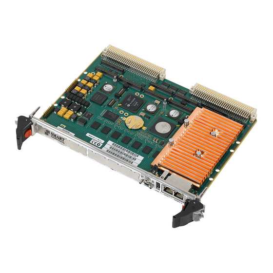
- Page 1 MVME7100 Single Board Computer Programmer’s Reference P/N: 6806800E82B June 2014...
- Page 2 Artesyn reserves the right to revise this document and to make changes from time to time in the content hereof without obligation of Artesyn to notify any person of such revision or changes.
-
Page 3: Table Of Contents
3.1.16 Watch Dog Timer Load Register ..........40 MVME7100 Single Board Computer Programmer’s Reference (6806800E82B) - Page 4 4.13.3 Local Bus Controller Clock Divisor ..........66 MVME7100 Single Board Computer Programmer’s Reference (6806800E82B)
- Page 5 A.10 VPD Contents for MVME7100 Boards ........
- Page 6 Contents Contents Contents MVME7100 Single Board Computer Programmer’s Reference (6806800E82B)
- Page 7 LBC Chip Select Assignments ........... . 58 MVME7100 Single Board Computer Programmer’s Reference (6806800E82B)
- Page 8 Variable SPD Contents ............88 Table B-1 Artesyn Embedded Technologies - Embedded Computing Publications ....95 Table B-2 Manufacturer’s Publications .
- Page 9 Boot Flash Bank ............32 MVME7100 Single Board Computer Programmer’s Reference (6806800E82B)
- Page 10 List of Figures MVME7100 Single Board Computer Programmer’s Reference (6806800E82B)
-
Page 11: About This Manual
IDSEL mapping, interrupt assignments for the MC864 D interrupt controller, Flash memory, two-wire serial interface addressing, and other device and system considerations. Appendix B, Related Documentation, provides a listing of related Artesyn manuals, vendor documentation, and industry specifications. Abbreviations This document uses the following abbreviations:... - Page 12 Repeated item for example node 1, node 2, ..., node 12 Omission of information from example/command that is not necessary at the time being Ranges, for example: 0..4 means one of the integers 0,1,2,3, and 4 (used in registers) MVME7100 Single Board Computer Programmer’s Reference (6806800E82B)
- Page 13 No danger encountered. Pay attention to important information Summary of Changes This is the first edition of this manual.. Part Number Publication Date Description 6806800E82A January 2009 First Release 6806800E82B June 2014 Re- branded to Artesyn template. MVME7100 Single Board Computer Programmer’s Reference (6806800E82B)
- Page 14 About this Manual About this Manual MVME7100 Single Board Computer Programmer’s Reference (6806800E82B)
-
Page 15: Introduction
D Reference Manual listed in Appendix B, Related Documentation, for more detail and programming information. At the time of publication of this manual, the MVME7100 Single Board Computer is available in the configurations shown below. Table 1-1 Board Variants Marketing #... - Page 16 PMC site 2 front I/O One four-channel USB 2.0 controller: one channel for front panel I/O Ethernet Four 10/100/1000 MC864xD Ethernet channels: two front panel Ethernet connectors and two channels for rear P2 I/O MVME7100 Single Board Computer Programmer’s Reference (6806800E82B)
- Page 17 User S/W controlled LED Planar status indicators One standard 16-pin JTAG/COP header Boundary scan support Switches for VME geographical addressing in a three-row backplane Software Support VxWorks OS support Linux OS support MVME7100 Single Board Computer Programmer’s Reference (6806800E82B)
-
Page 18: Block Diagram
Introduction Block Diagram The following figure is a block diagram of the MVME7100 architecture. MVME7100 Single Board Computer Programmer’s Reference (6806800E82B) - Page 19 Introduction Figure 1-1 Block Diagram MVME7100 Single Board Computer Programmer’s Reference (6806800E82B)
-
Page 20: Functional Description
I/O with access to the rear I/O via the MVME7216E transition module. The MVME7100 provides front panel access to one serial port with a mini DB-9 connector, two 10/100/1000 Ethernet ports with two RJ-45 connectors, and one USB port with one type A connector. -
Page 21: Memory Maps
Chapter 2 Memory Maps Overview The following sections describe the memory maps for the MVME7100. Refer to the MC864 Reference Manual for additional details and/or programming information. 2.1.1 Default Processor Memory Map The following table describes a default memory map from the point of view of the processor after a processor reset. -
Page 22: Pci Memory Map
The following table is the suggested PCI memory map for each PCI bus. This table reflects the address map implemented by the board level firmware at release time. Table 2-3 PCI Memory Map Processor Address Start Size Definition Notes 0000 0000 top_dram - 1 dram_size System Memory (on-board DRAM) MVME7100 Single Board Computer Programmer’s Reference (6806800E82B) -
Page 23: Vme Memory Map
Memory Maps 2.1.4 VME Memory Map The MVME7100 is fully capable of supporting both the PReP and the CHRP VME Memory Map examples with RAM size limited to 2 GB. MVME7100 Single Board Computer Programmer’s Reference (6806800E82B) - Page 24 Memory Maps MVME7100 Single Board Computer Programmer’s Reference (6806800E82B)
-
Page 25: Register Descriptions
Overview System resources including system control and status registers, external timers, and the QUART are mapped into a 16 MB address range accessible from the MVME7100 local bus via the MC864 D LBC. The memory map is defined in the following table including the LBC bank chip select used to decode the register. - Page 26 COM 2 (QUART channel 1) F201 1FFF F201 2000 - COM 3 (QUART channel 2) F201 2FFF F201 3000 - COM 4 (QUART channel 3) F201 3FFF F201 4000 - COM 5 (QUART channel 4) F201 4FFF MVME7100 Single Board Computer Programmer’s Reference (6806800E82B)
- Page 27 External PLD Tick Timer 4 Counter Register F202 004C - Reserved F2FF FFFF F203 0000 NAND Chip 1 Data Register F203 0001 - Reserved F203 0FFF F203 1000 NAND Chip 2 Data Register F203 1001 - Reserved F203 FFFF MVME7100 Single Board Computer Programmer’s Reference (6806800E82B)
-
Page 28: System Status Register
2. 32-bit write only. 3. Byte read/write capable. 3.1.1 System Status Register The MVME7100 has a System Status Register that is a read only register used to provide general board status information. Table 3-2 System Status Register System Status Register - 0xF200 0000... -
Page 29: System Control Register
A set condition indicates the switch is on. 3.1.2 System Control Register The MVME7100 has a System Control Register that provides general board control bits. Table 3-3 System Control Register System Control Register - 0xF200 0001 Field... -
Page 30: Status Indicator Register
3.1.3 Status Indicator Register The MVME7100 provides a Status Indicator Register that may be read by the system software to determine the state of the on-board status indicator LEDs or written to by system software to illuminate the corresponding on-board LEDs. -
Page 31: Nor Flash Control/Status Register
Reserved for future implementation 3.1.4 NOR Flash Control/Status Register The MVME7100 Flash Control/Status Register provides software controlled bank write protect and map select functions as well as boot block select, bank write protect, and activity status for the NOR flash. - Page 32 Memory Map Select. When this bit is cleared, the flash memory map is controlled by the Flash Boot Block Select switch (see the MVME7100 Installation and Use manual for switch settings). When the Map Select bit is set, boot block A is selected and mapped...
-
Page 33: Interrupt Register 1
Register Descriptions 3.1.5 Interrupt Register 1 The MVME7100 provides an Interrupt Register that may be read by the system software to determine which of the Ethernet PHYs originated their combined (OR'd) interrupt Table 3-6 Interrupt Register 1 Interrupt Register 1 - 0xF200 0004... -
Page 34: Presence Detect Register
Reserved for future implementation. 3.1.7 Presence Detect Register The MVME7100 provides a Presence Detect Register that may be read by the system software to determine the presence of optional devices. Table 3-8 Presence Detect Register Presence Detect Register - 0xF200 0006... -
Page 35: Nand Flash Chip 1 Control Register
Reserved for future implementation 3.1.8 NAND Flash Chip 1 Control Register The MVME7100 provides a Control Register for the NAND Flash device. Table 3-9 NAND Flash Chip 1 Control Register NAND Flash Chip 1 Control Register - 0xF200 0010 Field... -
Page 36: Nand Flash Chip 1 Select Register
Reserved for future implementation. 3.1.9 NAND Flash Chip 1 Select Register The MVME7100 provides a Select Register for the NAND Flash device. Table 3-10 NAND Flash Chip 1 Select Register NAND Flash Chip 1 Select Register - 0xF200 0011 Field... -
Page 37: Nand Flash Chip 1 Presence Register
Register Descriptions 3.1.10 NAND Flash Chip 1 Presence Register The MVME7100 provides a Presence Register for the NAND Flash device. Table 3-11 NAND Flash Chip 1 Presence Register NAND Flash Chip 1 Presence Register - 0xF200 0014 Field RSVD RSVD... -
Page 38: Nand Flash Chip 2 Control Register
RSVD Reserved for future implementation. 3.1.12 NAND Flash Chip 2 Control Register The MVME7100 provides a Control Register for the NAND Flash device. Table 3-13 NAND Flash Chip 2 Control Register NAND Flash Chip 2 Control Register - 0xF200 0018... -
Page 39: Nand Flash Chip 2 Presence Register
RSVD Reserved for future implementation. 3.1.14 NAND Flash Chip 2 Presence Register The MVME7100 provides a Presence Register for the NAND Flash device. Table 3-15 NAND Flash Chip 2 Presence Register NAND Flash Chip 2 Presence Register - 0xF200 001C... -
Page 40: Nand Flash Chip 2 Status Register
RSVD Reserved for future implementation. 3.1.15 NAND Flash Chip 2 Status Register The MVME7100 provides a Status Register for the NAND Flash device. Table 3-16 NAND Flash Chip 2 Status Register NAND Flash Chip 2 Status Register - 0xF200 001D... -
Page 41: Watch Dog Control Register
SYSRST System Reset. If cleared a board-level reset is generated when a time-out occurs. If set, a VMEbus SYSRST is generated when a time-out occurs. If MVME7100 is SYSCON then a local reset will also result in a VMEbus SYSRST. -
Page 42: Watch Dog Timer Resolution Register
Register Descriptions 3.1.18 Watch Dog Timer Resolution Register The MVME7100 provides a watch dog timer resolution register. Table 3-19 Watch Dog Timer count Register Watch Dog Timer Resolution Register - 0xF200 0025 Field RSVD RSVD RSVD RSVD OPER RESET Resolution. -
Page 43: Watch Dog Timer Count Register
If the counter reaches zero a system or board-level reset will be generated. 3.1.20 PLD Revision Register The MVME7100 provides a PLD revision register that can be read by the system software to determine the current revision of the timers/registers PLD. -
Page 44: Pld Date Code Register
8-bit field containing the current timer/register PLD revision. The revision number starts with 3.1.21 PLD Date Code Register The MVME7100 PLD provides a 32-bit register which contains the build date code of the inters/registers PLD. Table 3-22 PLD Date Code Register... -
Page 45: Test Register 2
TEST1. 3.1.24 External Timer Registers The MVME7100 provides a set of tick timer registers for access to the four external timers implemented in the timers/registers PLD. Note that these registers are 32-bit registers and are not byte writable. -
Page 46: Prescaler
Tick Timer 2 Control Register - 0xF202 0020 (32 bits) Tick Timer 3 Control Register - 0xF202 0030 (32 bits) Tick Timer 4 Control Register - 0xF202 0040 (32 bits) … Field … MVME7100 Single Board Computer Programmer’s Reference (6806800E82B) -
Page 47: Compare Register
If the clear-on-compare mode is enabled the counter is also cleared. For periodic interrupts this equation should be used to calculate the compare register value for a specific period (T): Compare register value=T (us) MVME7100 Single Board Computer Programmer’s Reference (6806800E82B) -
Page 48: Counter Register
Tick Timer 2 Counter Register - 0xF202 0028 (32 bits) Tick Timer 3 Counter Register - 0xF202 0038 (32 bits) Tick Timer 4 Counter Register - 0xF202 0048 (32 bits) … Field Tick Timer Counter Value OPER RESET MVME7100 Single Board Computer Programmer’s Reference (6806800E82B) -
Page 49: Geographical Address Register
The VMEbus Status Register in the Tsi148 provides the VMEbus geographical address of the MVME7100. This register reflects the inverted states of the geographical address pins at the 5- row, 160-pin P1 connector. Applications not using the 5-row backplane can use the planar switch described in the MVME7100 Installation and Use manual to assign a geographical address. - Page 50 Register Descriptions MVME7100 Single Board Computer Programmer’s Reference (6806800E82B)
-
Page 51: Programming Details
MC864xD Reset Configuration The MVME7100 supports the power-on reset (POR) pin sampling method for processor reset configuration. The states of the various configuration pins on the processor are sampled when reset is deasserted to determine the desired operating modes. Combinations of pull-up and pull-down resistors are used to set the options. -
Page 52: Table 4-1 Mc864Xd Por Configuration Settings
0_100 LA[27] the 1.3GHz MPX Clock) processor 0_110 2.5:1 0_1000 for 1_000 1.067GHz processor 1_110 3.5:1 1_010 0_111 4.5:1 TSEC3_TXD[2] Resistor Core 1 Enable Core 1 disabled (no option Core 1 enabled disabled) MVME7100 Single Board Computer Programmer’s Reference (6806800E82B) - Page 53 Local Bus GPCM - 16 1111 Local Bus GPCM -32 -bit TSEC1_TXD[0] Resistor 1 (no Alternate PCI-E 1 outbound ATMU option Boot Vector window 1 is enabled pulldown) Location Boot vector fetched from default boot ROM location MVME7100 Single Board Computer Programmer’s Reference (6806800E82B)
- Page 54 SerDes1: disabled SerDes2: x4 Serial RapidIO 1011 SerDes1: disabled SerDes2: x4 Serial RapidIO 1110 SerDes1: disabled SerDes2: x1/x2/x4/x8 PCIE 1111 SerDes1: x1/x2/x4/x8 PCI-E, 100 MHz ref clk SerDes2: x1/x2/x4/x8 PCI-E, 100 MHz ref clk MVME7100 Single Board Computer Programmer’s Reference (6806800E82B)
- Page 55 LGPL3, LGPL5 Testpoints Boot Normal I2C addressing Sequencer Extended I2C addressing Configuration Boot sequencer is disabled TSEC2_TXD[4] No Connects DDR SDRAM DDR1 Type TSEC2_TX_ER (default) DDR2 MVME7100 Single Board Computer Programmer’s Reference (6806800E82B)
- Page 56 D1_MSRCID[1] No Connect DDR Debug DDR debug information is Configuration driven on the ECC pins (processor instead of the normal ECC default) I/O. DDR debug information is not driven on the ECC pins. MVME7100 Single Board Computer Programmer’s Reference (6806800E82B)
-
Page 57: Mc864Xd Interrupt Controller
Programming Details MC864xD Interrupt Controller The MVME7100 uses the MC864xD integrated programmable interrupt controller (PIC) to manage locally generated interrupts. Currently defined external interrupting devices and interrupt assignments, along with corresponding edge/levels and polarities, are shown in the following table. -
Page 58: Local Bus Controller Chip Select Assignments
Not Used 1. Flash bank size determined by VPD flash packet. 2. Control/Status registers are byte read and write capable. 3. 32-bit timer registers are byte readable, but must be written as 32 bits. MVME7100 Single Board Computer Programmer’s Reference (6806800E82B) -
Page 59: I2C Device Addresses
MC864xD. The MC864xD I C controller is used by the system software to read the contents of the various I C devices located on the MVME7100. The following table contains the I C devices used for the MVME7100 and their assigned device addresses. -
Page 60: Vpd Eeprom
Programming Details VPD EEPROM The MVME7100 board provides an 8 KB dual address serial EEPROM containing Vital Product Data (VPD) configuration information specific to the MVME7100. Typical information that may be present in the EEPROM may include: manufacturer, board revision, build version, date of assembly, memory present, options present, L2 cache information, etc. -
Page 61: Flash Memory
Programming Details 4.10 Flash Memory The MVME7100 is designed to provide 128 MB of soldered-on NOR flash memory. Two AMD +3.0 V devices are configured to operate in 16-bit mode to form a 32-bit flash bank. This flash bank is also the boot bank and is connected to LBC Chip Select 0 and 1. The NOR flash is accessed via the MC864xD local bus. -
Page 62: Pci Idsel And Interrupt Definition
INTD INTA INTB (PEX8114) IRQ3 IRQ0 IRQ1 IRQ2 PCI4 0b0_0010 uPD720101 INTC INTA INTB (PEX8112) IRQ3 IRQ0 IRQ1 IRQ2 Refer to the MC864xD reference manual for additional details about the MC864xD PIC operation. MVME7100 Single Board Computer Programmer’s Reference (6806800E82B) -
Page 63: Pci Arbitration Assignments
The integrated PCI/X arbiters internal to the PEX8112 and the PEX8114 provide PCI arbitration for the MVME7100. The arbitration assignments on the MVME7100 are shown in the next table so that software may set arbiter priority assignments if necessary. Table 4-10 PCI Arbitration Assignments... -
Page 64: Lbc Timing Parameters
NAND NOR Flash NOR Flash Flash MRAM UART Timers BCTLD CSNT XACS SETA TRLX EHTR 4.12.2 USB Oscillator Configuration Software must configure the USB chip for the correct clock input of 48 MHz. MVME7100 Single Board Computer Programmer’s Reference (6806800E82B) -
Page 65: Clock Distribution
PCI-E clock. Additional clocks required by individual devices are generated near the devices using individual oscillators. The following table lists the clocks required on the MVME7100 along with their frequency and source. Table 4-12 Clock Assignments... -
Page 66: System Clock
MC864xD PIC timers which software can use as a known timing reference. 4.13.3 Local Bus Controller Clock Divisor The Local Bus Controller (LBC) clock output is connected to the PLD but is not used by the internal logic MVME7100 Single Board Computer Programmer’s Reference (6806800E82B) -
Page 67: Programmable Configuration Data
Overview This appendix provides data and specifications pertaining to programmable parts used on the MVME7100. The board is shipped after the programmable parts have been programmed through ATE or boundary scan according to the In-Circuit Test specifications. Table A-1 Programmable Devices... -
Page 68: Vital Product Data (Vpd) Introduction
Security information (VPD type, version and revision data, 32-bit CRC protection) How to Read and Modify VPD Information vpdDisplay may be used to display VPD information. vpdEdit can be used to modify the VPD information. MVME7100 Single Board Computer Programmer’s Reference (6806800E82B) -
Page 69: What Happens If Vpd Information Is Corrupted
The board may hang during startup (no-start condition). The board may be very unstable if it reaches the prompt. Device drivers, diagnostic tests and firmware commands may hang or fail in unexpected ways. MVME7100 Single Board Computer Programmer’s Reference (6806800E82B) -
Page 70: How To Fix Wrong Vpd Problems
If you suspect that your board has problems, as a result of wrong VPD information, select SAFE mode by setting S1:1 ON and reboot the MVME7100. At this point, the firmware will ignore all SROM contents. Use SROM or the IBM command to change the VPD to the correct parameters. - Page 71 (dataBitValue = 0; dataBitValue < 8; dataBitValue++) msbDataBitValue = (crcValue >> 31) & 1; crcValue <<= 1; if (msbDataBitValue ^ (dataByte & 1)) crcValue ^= 0x04c11db6; crcValue |= 1; dataByte >>= 1; crcValueFlipped = 0; MVME7100 Single Board Computer Programmer’s Reference (6806800E82B)
-
Page 72: Serial Presence Detect Checksum Calculation
The low order byte is the “Checksum”. Table A-3 Checksum Calculation Example SPD Byte Address Serial PD Convert to Decimal 00 (0x00) 0010 0100 > 01 (0x01) 1111 1110 > + 254 02 (0x02) 0000 0000 > MVME7100 Single Board Computer Programmer’s Reference (6806800E82B) - Page 73 > > > 60 (0x3C) 0000 0000 > 61 (0x3D) 0000 0000 > 62 (0x3E) 0000 0000 > Decimal Total Divide by 256 Remainder Convert to binary 0010 0010 < 63(0x3F)(Checksum) 0010 0010 MVME7100 Single Board Computer Programmer’s Reference (6806800E82B)
-
Page 74: Vpd Contents For Mvme7100 Boards
Data (HEX) Field Type Description ASCII Eye-Catcher ("Artesyn") Note: Lowest CRC byte for the calculation of CRC. BINARY Size of VPD area in bytes. The size is viewed as logical; it is not the size of the EEPROM. 512 bytes in this VPD... - Page 75 Table A-4 Static VPD Contents (continued) Offset (HEX) Data (HEX) Field Type Description ASCII Product Identifier. Refer to Table A-5. BINARY Factory Assembly Number. Refer to Notes and 2. BINARY # of bytes MVME7100 Single Board Computer Programmer’s Reference (6806800E82B)
- Page 76 **Serial number to be filled in. Refer to Notes and 3. BINARY # of bytes ASCII Most significant serial number character Least significant serial number character BINARY External Processor Clock Frequency Packet BINARY # of bytes MVME7100 Single Board Computer Programmer’s Reference (6806800E82B)
- Page 77 Ethernet Controller 0 BINARY Ethernet MAC Address Packet BINARY # of bytes BINARY Six bytes containing the next Ethernet address. BINARY Ethernet Controller 1 BINARY Ethernet MAC Address Packet BINARY # of bytes MVME7100 Single Board Computer Programmer’s Reference (6806800E82B)
- Page 78 Ethernet MAC Address Packet BINARY # of bytes BINARY Six bytes containing the highest Ethernet address. BINARY Ethernet Controller 3 BINARY Processor Identifier Packet BINARY # of bytes ASCII Processor type Refer to Table A-5. MVME7100 Single Board Computer Programmer’s Reference (6806800E82B)
- Page 79 Flash bank number BINARY Flash access speed in nanoseconds: 0x6E = 110 ns BINARY Total bank size [(1<<n)*256K bytes]: 0x09 = 128 MB BINARY Bank 2 Flash Memory Configuration Packet BINARY # of bytes MVME7100 Single Board Computer Programmer’s Reference (6806800E82B)
- Page 80 3. This data is not static. Each board's Serial Number packet must be unique. The board's serial number is obtained from the onboard serial number label. MVME7100 Single Board Computer Programmer’s Reference (6806800E82B)
-
Page 81: Table A-5 Variable Vpd Contents
0x32 represents the assembly revision letter (A=41, B=42, etc.). Table A-5 Variable VPD Contents Offset (Hex) MVME7100-161 MVME7100-163 MVME7100-171 MVME7100-173 0106839D01* 0106839D02* 0106839D03* 0106839D04* Product Identifier (ASCII) Factory Assembly Number (ASCII) MVME7100 Single Board Computer Programmer’s Reference (6806800E82B) - Page 82 Programmable Configuration Data Table A-5 Variable VPD Contents (continued) Offset (Hex) MVME7100-161 MVME7100-163 MVME7100-171 MVME7100-173 0106839D01* 0106839D02* 0106839D03* 0106839D04* Processor Type NAND Flash Size MVME7100 Single Board Computer Programmer’s Reference (6806800E82B)
-
Page 83: Spd Contents For Mvme7100 Boards
Refresh Rate/Type: 0x82 = 7.8us. Refer to Notes 3 and 4. 13 (0x0D) Primary SDRAM Width: 0x08 = 8 bits 14 (0x0E) Error Checking SDRAM Width: 0x08 = 8 bits 15 (0x0F) Reserved MVME7100 Single Board Computer Programmer’s Reference (6806800E82B) - Page 84 Minimum RAS to CAS delay (t RCD): 0x3C = 15ns. Refer to Note 3. 30 (0x1E) Minimum RAS Pulse width (t RAS): 0x2D = 45ns. Refer to Note 3. 31 (0x1F) Module Bank Density: 0x80 = 512 MB MVME7100 Single Board Computer Programmer’s Reference (6806800E82B)
- Page 85 Tcasemax: 0x50 = 95 degree max case temperature 48 (0x30) Not Used 49 (0x31) 0x03 = Double refresh mode bit and High temperature self-refresh 50 (0x32) Not Used 51 (0x33) Not Used 52 (0x34) Not Used 53 (0x35) Not Used MVME7100 Single Board Computer Programmer’s Reference (6806800E82B)
- Page 86 66 (0x42) 67 (0x43) 68 (0x44) 69 (0x45) 70 (0x46) 71 (0x47) 72 (0x48) Module Manufacturing location. Refer to Note 5. 73 (0x49) Module Part Number. Refer to Note 5. 74 (0x4A) 75 (0x4B) MVME7100 Single Board Computer Programmer’s Reference (6806800E82B)
- Page 87 Module Manufacturing Date. Refer to Note 5. 94 (0x5E) 95 (0x5F) Module Serial Number. Refer to Note 5. 96 (0x60) 97 (0x61) 98 (0x62) 99 (0x63) Manufacturer's Specific Data. Refer to Note 5. MVME7100 Single Board Computer Programmer’s Reference (6806800E82B)
-
Page 88: Table A-7 Variable Spd Contents
Reserved 08 (0x08) Voltage Interface Level of this assembly: 0x05 = SSTL 1.8 V 09 (0x09) SDRAM Cycle time at Maximum Supported CAS Latency (CL), CL=X: 0x30 = 3.0ns. Refer to Note 3. MVME7100 Single Board Computer Programmer’s Reference (6806800E82B) - Page 89 25 (0x19) Minimum Clock Cycle at CLX-2: 0x50 = 5.0 Ns. Refer to Note 3. 26 (0x1A) Maximum Data Access Time (t AC) from Clock at CLX-2: 0x60 = 0.60ns. Refer to Note 3. MVME7100 Single Board Computer Programmer’s Reference (6806800E82B)
- Page 90 Maximum Cycle Time (t CK max) 0x80 = 8ns 44 (0x2C) DQS-DQ Skew for DQS and associated DQ signals (t DQSQ max) 0x18 = 0.240ns 45 (0x2D) Read Data Hold Skew Factor (t QHS) 0x22 = 0.340ns MVME7100 Single Board Computer Programmer’s Reference (6806800E82B)
- Page 91 63 (0x3F) Checksum for bytes 0 - 62. Refer to Section 0 64 (0x40) Manufactures JEDEC ID Code. Refer to Note 5. 65 (0x41) 66 (0x42) 67 (0x43) 68 (0x44) 69 (0x45) 70 (0x46) MVME7100 Single Board Computer Programmer’s Reference (6806800E82B)
- Page 92 85 (0x55) 86 (0x56) 87 (0x57) 88 (0x58) 89 (0x59) 90 (0x5A) 91 (0x5B) Module Revision Code. Refer to Note 5. 92 (0x5C) 93 (0x5D) Module Manufacturing Date. Refer to Note 5. 94 (0x5E) MVME7100 Single Board Computer Programmer’s Reference (6806800E82B)
- Page 93 1. This will typically be programmed as 128 bytes. 2. his will typically be programmed as 256 bytes. 3. From datasheet. 4. High order bit is Self refresh “flag”. If set to “1”, the assembly supports self refresh. 5. Reserved. MVME7100 Single Board Computer Programmer’s Reference (6806800E82B)
- Page 94 Programmable Configuration Data MVME7100 Single Board Computer Programmer’s Reference (6806800E82B)
-
Page 95: Related Documentation
The publications listed below are referenced in this manual. You can obtain electronic copies of Artesyn Embedded Technologies - Embedded Computing publications by contacting your local Artesyn sales office. For released products, you can also visit our Web site for the latest copies of our product documentation. - Page 96 Freescale MR2A16AVYS35 512 KB MRAM Texas Instruments Data Sheet SCES357E SN74VMEH22501 Revised March 2004 8-bit Universal Bus Transceiver and Two 1-bit Bus Transceivers with Split LVTTL Port, Feedback Path, and 3-state Outputs Exar MVME7100 Single Board Computer Programmer’s Reference (6806800E82B)
- Page 97 FN 80A3020_ MA001_08 Broadcom Corporation BCM5482S 5482S-DS06-R 10/100/1000BASE-T Gigabit Ethernet Transceiver 2/15/07 PLX Technology PEX 8112AA Version 1.2 ExpressLane PCI Express-to-PCI Bridge Data Book ExpressLane PEX 8114BC Version 3.0 PCI Express-to-PCI/PCI-X Bridge Data Book MVME7100 Single Board Computer Programmer’s Reference (6806800E82B)
-
Page 98: Related Specifications
Connector Current Capacity ANSI/VITA 1.7-2003 Universal Serial Bus Universal Serial Bus Specification Revision 2.0 April 27, 2000 PCI Special Interest Group PCI Local Bus Specification, Revision 2.2 PCI Rev 2.2 December 18, 1998 MVME7100 Single Board Computer Programmer’s Reference (6806800E82B) - Page 99 Institute for Electrical and Electronics Engineers, Inc. Draft Standard for a Common Mezzanine P1386 - 2001 Card Family: CMC Draft Standard Physical and P1386 - 2001 Environmental Layer for PCI Mezzanine Cards: PMC MVME7100 Single Board Computer Programmer’s Reference (6806800E82B)
- Page 100 Related Documentation MVME7100 Single Board Computer Programmer’s Reference (6806800E82B)
- Page 102 Artesyn Embedded Technologies, Artesyn and the Artesyn Embedded Technologies logo are trademarks and service marks of Artesyn Embedded Technologies, Inc. All other product or service names are the property of their respective owners. © 2014 Artesyn Embedded Technologies, Inc.
Need help?
Do you have a question about the MVME7100 and is the answer not in the manual?
Questions and answers