Sign In
Upload
Manuals
Brands
Artesyn Manuals
Motherboard
MVME5100
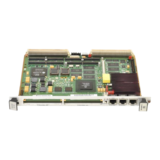
User Manuals: Artesyn MVME5100 VME Embedded Controller
Manuals and User Guides for Artesyn MVME5100 VME Embedded Controller. We have
1
Artesyn MVME5100 VME Embedded Controller manual available for free PDF download: Programmer's Reference Manual
Artesyn MVME5100 Programmer's Reference Manual (318 pages)
Brand:
Artesyn
| Category:
Motherboard
| Size: 20 MB
Table of Contents
Table of Contents
3
List of Figures
16
About this Manual
17
Summary of Changes
24
1 Product Data and Memory Maps
25
Features
25
Figure 1-1 MVME5100 Block Diagram
27
Memory Maps
28
Processor Memory Map
28
Table 1-2 Default Processor Memory Map
29
Table 1-3 Suggested CHRP Memory Map
30
Table 1-4 Hawk PPC Register Values for Suggested Memory Map
31
Pci Memory Map
31
PCI Local Bus Memory Map
32
Vmebus Memory Map
32
System Bus
32
Processors
33
Processor Type Identification
33
Processor PLL Configuration
34
L2 Cache
34
L2 Cache SRAM Size
34
Cache Speed
34
FLASH Memory
35
ECC Memory
35
P2 I/O Modes
36
Serial Presence Detect (SPD) Definitions
36
Hawk ASIC
36
Hawk I2C Interface and Configuration Information
37
Vital Product Data (VPD) and Serial Presence Detect (SPD) Data
38
Table 1-5 I2C Device Addressing
38
PCI Local Bus
39
MODFAIL Bit Register
39
TBEN Bit Register
39
PCI Arbitration Assignments for Hawk ASIC
40
Table 1-6 PCI Arbitration Assignments
40
The Ethernet Controller
40
Figure 1-2 PMC/PCI Expansion Slots
41
PMC/PCI Expansion Slots
41
Figure 1-3 Vmebus Master Mapping
42
The Universe ASIC
42
PCI Configuration Space
43
Table 1-7 IDSEL Mapping for PCI Devices
43
Hawk External Register Bus Address Assignments
44
Table 1-8 On-Board PCI Device Identification
44
Table 1-9 Hawk External Register Bus Summary
45
Dual TL16C550 Uarts
46
Status Register
47
Table 1-10 16550 Access Registers
47
MODFAIL Bit Register
48
Table 1-11 MVME5100 Status Register
48
MODRST Bit Register
49
Table 1-13 MODRST Bit Register
49
TBEN Bit Register
50
NVRAM/RTC & Watchdog Timer
51
Table 1-15 M48T37V Access Registers
51
Software Readable Header/Switch Register (S1)
52
Table 1-16 Software Readable Header/Switch Register (S1)
52
Figure 1-4 SRH Pin Assignments
53
Geographical Address Register (VME Board)
53
Table 1-17 Geographical Address Register (VME Board)
53
Extended Features Register 1
54
Table 1-18 Extended Features Register 1
54
Board Last Reset Register
55
Table 1-19 Board Last Reset Register
55
Extended Features Register 2
56
Ipmc7Xx ISA Bus Resources
56
Table 1-20 Extended Features Register 2
56
PC87308VUL Super I/O (ISASIO) Strapping
57
Table 1-21 Strap Pins Configuration for the PC87308VUL
57
W83C554 PIB Registers
57
Z85230 ESCC and Z8536 CIO Registers and Port Pins
57
Table 1-22 Z8536/Z85230 Access Registers
58
Table 1-23 Z8536 CIO Port Pins Assignment
58
Table
59
Table 1-24 Interpretation of MID3-MID0
60
ISA DMA Channels
61
Table 1-25 PIB DMA Channel Assignments
61
2 Hawk PCI Host Bridge & Multi-Processor Interrupt Controller
63
Overview
63
Features
63
Table 2-1 2Hawk PCI Host Bridge & Multi-Processor Interrupt Controller
63
Block Diagram
65
Figure 2-1 Hawk PCI Host Bridge Block Diagram
65
Functional Description
66
Architectural Overview
66
PPC Bus Interface
67
Figure 2-2 PPC to PCI Address Decoding
68
Figure 2-3 PPC to PCI Address Translation
69
Table 2-2 PPC Slave Response Command Types
70
Table 2-3 PPC Master Transaction Profiles and Starting Offsets
72
Table 2-4 PPC Master Write Posting Options
73
Table 2-5 PPC Master Read Ahead Options
74
Table 2-6 PPC Master Transfer Types
75
Table 2-7 PPC Arbiter Pin Assignments
76
PCI Bus Interface
79
Figure 2-4 PCI to PPC Address Decoding
80
Figure 2-5 PCI to PPC Address Translation
81
Figure 2-6 PHB Address Decoder Priority
81
Table 2-8 PCI Slave Response Command Types
82
Table 2-9 PCI Master Command Codes
86
Figure 2-7 PCI Spread I/O Address Translation
90
Table 2-11 Device Number Decoding
91
Table 2-54 Table
91
Table 2-12 PCI Arbiter Pin Description
93
Table 2-13 Fixed Mode Priority Level Setting
94
Table 2-14 Mixed Mode Priority Level Setting
95
Table 2-15 Arbitration Setting
96
Endian Conversion
97
Figure 2-8 Big-To-Little-Endian Data Swap
98
Table 2-16 Address Modification for Little Endian Transfers
99
Error Handling
100
Watchdog Timers
101
Table 2-18 Wdtxcntl Programming
102
PCI/PPC Contention Handling
104
Transaction Ordering
106
PHB Hardware Configuration
108
Table 2-19 PHB Hardware Configuration
108
Multi-Processor Interrupt Controller (MPIC)
109
MPIC Features
109
Architecture
110
External Interrupt Interface
110
Csr's Readability
111
Interrupt Source Priority
111
Figure 2-9 Serial Mode Interrupt Scan
111
Processor's Current Task Priority
112
Nesting of Interrupt Events
112
Spurious Vector Generation
112
Interprocessor Interrupts (IPI)
112
8259 Compatibility
113
Hawk Internal Error Interrupt
113
Timers
113
Interrupt Delivery Modes
114
Block Diagram Description
114
Figure 2-10 MPIC Block Diagram
116
Programming Notes
119
Operation
121
Architectural Notes
123
Effects of Interrupt Serialization
123
Registers
124
PPC Registers
124
Table 2-23 Revision ID Register
124
Table 2-20 PPC Register Map for PHB
125
Table 2-44 PCI Interrupt Acknowledge Register
125
Table 2-21 Vendor ID/Device ID Registers
126
Revision ID Register
127
Time-Out Length
129
Ppc ID
129
PPC Arbiter/Pci Arbiter Control Registers
130
Flatten Single Write Field
130
Parking Field
131
Priority Field
132
Parking Field
132
Table
133
Hierarchy Field
133
Hierarchy Field - Mixed Priority Scheme
133
Table 2-33 Hardware Control-Status/Prescaler Adjust Register
134
PPC/PCI Clock Ratio Field
135
Write Lock Resolution Threshold
135
Read Lock Resolution Threshold
136
Table 2-37 Common Scale Factors for Common CLK Frequencies
136
PPC Error Test/Error Enable Register
137
Table 2-39 PPC Error Status Register
140
PPC Error Address Register
141
PPC Error Attribute Register
142
PPC Error Attribute Register, PSMA or PRTA Set
143
PCI Interrupt Acknowledge Register
144
PPC Slave Offset/Attribute (0, 1 and 2) Registers
145
PPC Slave Address (3) Register
146
PPC Slave Offset/Attribute (3) Registers
147
Wdtxcntl Registers
148
RES Field Options
149
Wdtxstat Registers
151
PCI Registers
152
Table 2-48 Table
152
General Purpose Registers
152
PCI Configuration Register
152
Table
153
PCI I/O Register
153
Vendor ID/ Device ID Registers
154
PCI Command/ Status Registers
154
Revision ID/ Class Code Registers
156
Header Type Register
157
MPIC I/O Base Address Register
158
MPIC Memory Base Address Register
158
PCI Slave Address (0,1,2, and 3) Registers
160
PCI Slave Attribute/ Offset (0,1,2 and 3) Registers
161
Rmftx Field
162
Wxftx Field
162
Table 2-64 Conceptual Perspective from the PCI Bus
163
Table 2-65 Perspective from the PPC Bus in Big Endian Mode
163
Table 2-66 Perspective from the PPC Bus in Little Endian Mode
164
Table 2-67 Conceptual Perspective from the PCI Bus
165
Table 2-68 Perspective from the PPC Bus in Big Endian Mode
165
MPIC Registers
166
Table 2-69 Perspective from the PPC Bus in Little Endian Mode
166
MPIC Register Map
167
Feature Reporting Register
169
Global Configuration Register
170
Cascade Mode Encoding
171
Tie Mode Encoding
171
Vendor Identification Register
172
Processor Init Register
172
IPI Vector/Priority Registers
173
Spurious Vector Register
174
Timer Frequency Register
174
Timer Current Count Registers
175
Timer Basecount Registers
176
Timer Vector/Priority Registers
177
Timer Destination Registers
178
External Source Vector/Priority Registers
178
External Source Destination Registers
180
Table 2-86 Hawk Internal Error Interrupt Vector/Priority Register
180
Hawk Internal Error Interrupt Destination Register
182
Interprocessor Interrupt Dispatch Registers
182
Current Task Priority Registers
183
Interrupt Acknowledge Registers
184
End-Of-Interrupt Registers
184
3 System Memory Controller (SMC)
187
Overview
187
Bit Ordering Convention
187
Features
187
Block Diagrams
189
Figure 3-1 Hawk Used with Synchronous DRAM in a System
189
Figure 3-2 Hawk's System Memory Controller Internal Data Paths
190
Figure 3-3 Overall SDRAM Connections (4 Blocks Using Register Buffers)
191
Functional Description
192
Figure 3-4 Hawk's System Memory Controller Block Diagram
192
SDRAM Accesses
193
Ppc60X Bus Interface
196
SDRAM Organization
196
Sdram Ecc
198
Error Reporting
199
Error Logging
200
Rom/Flash Interface
201
Ppc60X to Rom/Flash (16 Bit Width) Address Mapping
202
Ppc60X to Rom/Flash (64 Bit Width) Address Mapping
204
Ppc60X Bus to Rom/Flash Access Timing (120Ns @ 100 Mhz)
206
Table
206
Table 2-52 Table
206
Ppc60X Bus to Rom/Flash Access Timing (50Ns @ 100 Mhz)
207
Ppc60X Bus to Rom/Flash Access Timing (80Ns @ 100 Mhz)
207
I2C Interface
208
Ppc60X Bus to Rom/Flash Access Timing (30Ns @ 100 Mhz)
208
Figure 3-5 Programming Sequence for I2C Byte Write
212
Figure 3-6 Programming Sequence for I2C Random Read
215
Figure 3-7 Programming Sequence for I2C Current Address Read
218
Figure 3-8 Programming Sequence for I2C
221
Figure 3-9 Programming Sequence for I2C Sequential Read
225
Chip Configuration
226
CSR Accesses
226
External Register Set
226
Refresh/Scrub
226
Programming Model
227
CSR Architecture
227
Register Summary
228
Detailed Register Bit Descriptions
230
Table 3-10 Possible Operations for each Bit in the Register
230
Table 3-11 Possible States of the Bits
230
Vendor/Device Register
232
Revision ID/General Control Register
232
SDRAM Enable and Size Register (Blocks A, B, C, D)
234
Table 3-15 Block_A/B/C/D/E/F/G/H Configurations
235
SDRAM Base Address Register (Blocks A/B/C/D)
236
CLK Frequency Register
237
Table 3-18 DRR and CLK Frequency Examples
238
ECC Control Register
239
Figure 3-10 Read/Write Check-Bit Data Paths
240
Error Logger Register
243
Error_Address Register
244
Scrub/Refresh Register
245
Scrub Address Register
246
ROM a Base/Size Register
247
Table 3-25 ROM Block a Size Encoding
248
Table 3-26 Rom_A_Rv and Rom_B_Rv Encoding
248
Table 3-27 Read/Write to Rom/Flash
249
ROM B Base/Size Register
250
Table
251
ROM Block B Size Encoding
251
ROM Speed Attributes Registers
252
Table 3-31 ROM Speed Bit Encoding
252
Data Parity Error Log Register
253
Data Parity Error Address Register
254
Data Parity Error Upper Data Register
255
Data Parity Error Lower Data Register
255
I2C Clock Prescaler Register
256
I2C Control Register
256
I2C Status Register
257
I2C Transmitter Data Register
258
I2C Receiver Data Register
259
SDRAM Enable and Size Register (Blocks E,F,G,H)
260
SDRAM Base Address Register (Blocks E/F/G/H)
261
SDRAM Speed Attributes Register
262
Trc Encoding
263
Tras Encoding
264
Address Parity Error Log Register
265
Address Parity Error Address Register
266
32-Bit Counter
266
External Register Set
267
Tben Register
268
Software Considerations
269
Table
269
Initializing SDRAM Related Control Registers
270
Table 3-55 Single Bit Errors Ordered by Syndrome Code
280
ECC Codes
280
MPIC Interrupt Assignments
283
Pci Arbitration
283
Interrupts
285
Table 4-2 PBC ISA Interrupt Assignments
285
Exceptions
286
Error Notification and Handling
287
Soft Reset
287
Endian Issues
288
Figure 4-1 Big-Endian Mode
289
Figure 4-2 Little-Endian Mode
290
Processor/Memory Domain
290
Pci Domain
291
A.1 Vital Product Data (VPD) Introduction
293
A.1.1 How to Read the VPD Information
294
A.1.3 What Happens if the VPD Information Is Corrupted
295
A.1.6 How to Fix Wrong VPD Problems
296
VPD Packet Types
296
A.1.8 VPD Definitions - Product Configuration Options Data
298
Table A-2 MCG Product Configuration Options Data
299
FLASH Memory Configuration Data
301
L2 Cache Configuration Data
302
VPD Revision Data
304
Table A-6 Example of a Checksum Calculation
307
B.1 Introduction
309
Table B-1 MVME2700/MVME5100 Sample Slave Image Settings
309
Related Documentation
313
Table C-1 Artesyn Embedded Technologies - Embedded Computing Publications
313
C.2 Manufacturer's Documents
314
C.3 Related Specifications
315
Advertisement
Advertisement
Related Products
Artesyn MVME5500
Artesyn MVME55006E
Artesyn MVME4100
Artesyn MVME6100
Artesyn MVME8105
Artesyn MVME8110
Artesyn MVME2500-0173
Artesyn MVME2500-02120201E
Artesyn MVME2500-0161
Artesyn MVME2500ET-0171
Artesyn Categories
Motherboard
Server
Single board computers
PCI Card
Computer Hardware
More Artesyn Manuals
Login
Sign In
OR
Sign in with Facebook
Sign in with Google
Upload manual
Upload from disk
Upload from URL