
Related Manuals for Advantech PCM-4380F-M0A2E


Summary of Contents for Advantech PCM-4380F-M0A2E
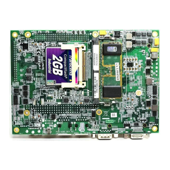
- Page 1 PCM-4380 Pentium® M 4" EPIC SBC with MIO/VGA/LCD/LVDS Ethernet/ USB2.0 and SSD User Manual...
- Page 2 Silicon Motion, Inc. Creative is a trademark of Creative Technology LTD. All other product names or trademarks are properties of their respective owners. For more information on this and other Advantech products, please visit our websites at: http://www.advantech.com http://www.advantech.com/eplatform For technical support and service, please visit our support website at: http://www.advantech.com/support...
- Page 3 Model Number Description PCM-4380F-S4A2E Pentium M 1.4GHz(2M L2) w/Dual LAN/VGA/ LCD/CFC PCM-4380F-S0A2E Celeron M 1.0GHz(512K L2) w/Dual LAN/VGA/ LCD/CFC PCM-4380F-M0A2E Celeron M 600MHz(512K L2) w/Dual LAN/VGA/ LCD/CFC PCM-4380Z2-S0A2E PCM-4380F-S0A2E with phoenix platinum pack- PCM-4380Z2-S4A2E PCM-4380F-S4A2E with phoenix platinum pack-...
- Page 4 PCM-410C-00A1E COM/LPT daughter board for EPIC Additional Information and Assistance Visit the Advantech web site at www.advantech.com where you can find the latest information about the product. Contact your distributor, sales representative, or Advantech's cus- tomer service center for technical support if you need additional assistance.
- Page 5 This device complies with the requirements in part 15 of the FCC rules: Operation is subject to the following two conditions: This device may not cause harmful interference, and This device must accept any interference received, including inter- ference that may cause undesired operation This equipment has been tested and found to comply with the limits for a Class A digital device, pursuant to Part 15 of the FCC Rules.
- Page 6 PCM-4380 User Manual...
-
Page 7: Table Of Contents
Contents Chapter 1 General Information ........2 Introduction ............... 2 Specifications ..............2 1.2.1 Standard 4" Biscuit SBC Functions........ 2 1.2.2 VGA/LVDS Interface ............. 3 1.2.3 Ethernet Interface............3 1.2.4 Audio Function ............... 3 1.2.5 Mechanical and Environmental ........4 Board layout and dimensions ..........5 Figure 1.1 Board layout: Dimensions (Component Side) ............ - Page 8 2.11.2 System FAN (CN5) ............16 2.12 Audio interfaces (CN31) ..........16 2.12.1 Audio connector (CN31) ..........16 2.13 COM port connector (CN21,CN30)........ 16 2.13.1 COM2 RS-232/422/485 setting (J3) ......16 Table 2.8 J3: COM2 RS-232/422/485 select..16 2.14 VGA/LCD/LVDS interface connections ......17 2.14.1 CRT display connector (CN16) ........
- Page 9 4.5.2 On-Chip Secondary PCI IDE........32 Figure 4.4 Integrated peripherals ......32 4.5.3 USB Controller ............32 4.5.4 USB Keyboard/Mouse Support ........32 4.5.5 AC97 Audio..............32 4.5.6 Init Display First ............32 4.5.7 IDE HDD Block Mode ..........33 4.5.8 Onboard Serial Port ............
- Page 10 5.2.2 AU M170EG01 (1024x768 LVDS LCD @ 36bit)..44 Table 5.2 Connections to AU M170EG01 (CN1) .. 44 Installation of the SVGA Driver ........45 5.3.1 Installation of Windows 2000........45 Further Information ............48 Chapter 6 Audio Setup.............50 Introduction ..............50 Driver installation............
- Page 11 LAN2(RJ45) (CN9)............72 Table A.7 LAN2(RJ45+10/100 Transformer) (CN9) ........... 72 Compact II without Ejector (CN11)........ 73 Table A.8 Compack II W/Ejector (CN11)....73 HD & Power LED (CN13)..........74 Table A.9 HD & Power LED (CN13) ..... 74 LVDS Connector (CN14)..........75 A.10 Table A.10 LVDS Connector (CN14).......
- Page 12 PCM-4380 User Manual...
- Page 13 General Information This chapter gives background infor- mation on the PCM-4380.
-
Page 14: Chapter 1 General Information
Chapter 1 General Information 1.1 Introduction The PCM-4380 is an EPIC SBC (Single Board Computer) with a high performance and lower power based on Pentium M/Celeron M proces- sors. The PCM-4380, in conjunction with Intel 855GME chipset, sup- ports processors clocked at up to 1.4 GHz, four USB 2.0 compatible ports, up to 2 PCI Fast or Gigabit Ethernet interface, 2 Channel LVDS interface and can accommodate up to 1 GB of DDR RAM memory. -
Page 15: Vga/Lvds Interface
• Keyboard/mouse connector: Supports one standard PC/AT key- board and a PS/2 mouse • Audio: Support AC 97 Audio Interface (with PCM-410A-00A1E option) • USB: 4 USB 2.0 compliant universal serial bus ports • Solid State Disk (SSD): Supports one 50-pin socket for CFC type I/II (PCM-4380F series only) 1.2.2 VGA/LVDS Interface... -
Page 16: Mechanical And Environmental
1.2.5 Mechanical and Environmental • Dimensions: 115 x 165 mm (4.5" x 6.5") Mechanical Drawing (dxf file) is available. • Power Supply Type: ATX, AT • Power Requirement: – ATX: +5 V ±5%, ±12 V ±5% (optional) – AT: 5 V only to boot up, 12 V for LCD inverter and PC/104 module (12 V optional for PC104 add on card and LCD inverter) •... -
Page 17: Board Layout And Dimensions
1.3 Board layout and dimensions Figure 1.1: Board layout: Dimensions (Component Side) Figure 1.2: Board layout: Dimensions (Solder Side) Chapter 1... - Page 18 PCM-4380 User Manual...
- Page 19 Installation This chapter explains the setup proce- dures of the PCM-4380 hardware, including instructions on setting jump- ers and connecting peripherals, switches and indicators. Be sure to read all safety precautions before you begin the installation procedure. Sections include:...
-
Page 20: Chapter 2 Installation
Chapter 2 Installation 2.1 Jumpers The PCM-4380 has a number of jumpers that allow you to configure your system to suit your application. The table below lists the functions of the various jumpers. 2.1.1 Jumper Location Table 2.1: Jumpers Label Function AT/ATX Power Select LCD Power... -
Page 21: Com2 Setting (J3)
Table 2.4: COM2 Setting (J3) Setting Function (1-2) RS232 (3-4) RS485 (5-6) RS422 Table 2.5: PCI-VIO Setting (J4) Setting Function +5 V +3.3 V Warning! To avoid damaging the computer, always turn off the power supply before setting “Clear CMOS.” Before turning on the power supply, set the jumper back to “3.0 V Battery On.”... -
Page 22: Connectors
2.2 Connectors On-board connectors link the PCM-4380 to external devices such as hard disk drives, a keyboard, or floppy drives. The table below lists the func- tion of each of the board’s connectors. Table 2.7: Connectors Label Function Power Con. DDR-SODIMM(RVS)-5.2 mm Battery Con. -
Page 23: Locating Connectors
2.3 Locating Connectors Figure 2.1: Connectors (component side) Figure 2.2: Connectors (solder side) Chapter 2... -
Page 24: Setting Jumpers
2.4 Setting Jumpers You may configure your card to match the needs of your application by setting jumpers. A jumper is a metal bridge used to close an electric cir- cuit. It consists of two metal pins and a small metal clip (often protected by a plastic cover) that slides over the pins to connect them. -
Page 25: Installing So-Dimm
2.5 Installing SO-DIMM Module Key Aligned With housing Key Housing Card Slot PC Board Module Tilted Approximately 25 Module Latching Ledge(TO Engage Edge of Module) The procedures for installing SODIMMs are described below. Please fol- low these steps carefully. You can install SDRAM memory modules using 200-pin SODIMMs (Small Outline Dual In-line Memory Modules). -
Page 26: Ide, Cdrom Hard Drive Connector (Cn27)
2.6 IDE, CDROM hard drive connector (CN27) The board provides 1 IDE channels which you can attach up to two Enhanced Integrated Device Electronics hard disk drives or CDROM to the board’s internal controller. Its IDE controller uses a PCI interface. This advanced IDE controller supports faster data transfer, PIO mode 3, mode 4 and up to UDMA/33. -
Page 27: Parallel Port Connector (Cn30)
2.8 Parallel port connector (CN30) Normally, the parallel port is used to connect the card to a printer. The board includes a multi-mode (ECP/EPP/SPP) parallel port accessed via CN30 and a 50-pin flat-cable connector. You will need an adapter cable if you use a traditional DB-25 connector. -
Page 28: Power Connectors (Cn1)
2.11 Power connectors (CN1) 2.11.1 Main power connector, +3.3V, +5 V, +12 V (CN1) Supplies main power to the PCM-4380 (+5 V), and to devices that require +12 V. 2.11.2 System FAN (CN5) 2.12 Audio interfaces (CN31) 2.12.1 Audio connector (CN31) The board provides all major audio signals and it can be optional with Line-in/Line-out/Speaker-out function by PCM-410A-00A1E. -
Page 29: Vga/Lcd/Lvds Interface Connections
2.14 VGA/LCD/LVDS interface connections The board’s PCI SVGA interface can drive conventional CRT displays and is capable of driving a wide range of flat panel displays, including passive LCD and active LCD displays. The board has two connectors to support these displays: one for standard CRT VGA monitors, one for flat panel displays, and one for LVDS type LCD panels. -
Page 30: Usb Connectors (Cn31,Cn18)
2.17 USB connectors (CN31,CN18) The board provides up to four USB (Universal Serial Bus) ports. This gives complete Plug and Play, and hot attach/detach for up to 127 external devices. The USB interfaces comply with USB specification Rev. 2.0 which supports 480Mbps transfer rate, and are fuse protected. The USB interface is accessed through one 8 x 2-pin flat-cable connec- tors, CN31 (USB0, 1). - Page 31 Chipset Software Installation Utility...
-
Page 32: Chapter 3 Chipset Software Installation Utility
Chapter 3 Chipset Software Installation Utility 3.1 Before you begin To facilitate the installation of the enhanced display device drivers and utility software, you should read the instructions in this chapter carefully before you attempt installation. The device drivers for the PCM-4380 board are located on the software installation CD. -
Page 33: Introduction
3.2 Introduction The Intel® Chipset Software Installation (CSI) utility installs to the target system the Windows INF files that outline to the operating system how the chipset components will be configured. This is needed for the proper functioning of the following features: •... - Page 34 Click "Next" when you see the following message. Click "Yes" when you see the following message. PCM-4380 User Manual...
- Page 35 Click "Next" when you see the following message. When the following message appears, click "Finish" to complete the installation and restart Windows. Chapter 3...
- Page 36 PCM-4380 User Manual...
- Page 37 Award BIOS Setup...
-
Page 38: Chapter 4 Award Bios Setup
Chapter 4 Award BIOS Setup 4.1 Introduction Award’s BIOS ROM has a built-in setup program that allows users to modify the basic system configuration. This type of information is stored in battery-backed memory (CMOS RAM) so that it retains the setup information when the power is turned off. -
Page 39: Entering Setup
4.2 Entering Setup Turn on the computer and check for the “patch code”. If there is a number assigned to the patch code, it means that the BIOS supports your CPU. If there is no number assigned to the patch code, please contact Advan- tech’s applications engineer to obtain an up-to-date patch code file. -
Page 40: Standard Cmos Setup
4.3 Standard CMOS Setup Choose the “Standard CMOS Features” option from the “Initial Setup Screen” menu, and the screen below will be displayed. This menu allows users to configure system components such as date, time, hard disk drive, floppy drive, display, and memory. Figure 4.2: Standard CMOS features screen PCM-4380 User Manual... -
Page 41: Advanced Bios Features
4.4 Advanced BIOS Features The “Advanced BIOS Features” screen appears when choosing the “Advanced BIOS Features” item from the “Initial Setup Screen” menu. It allows the user to configure the PCM-4380 according to his particular requirements. Below are some major items that are provided in the Advanced BIOS Features screen. -
Page 42: Quick Power On Self Test
4.4.3 Quick Power On Self Test This option speeds up the Power-On Self Test (POST) conducted as soon as the computer is turned on. When enabled, BIOS shortens or skips some of the items during the test. When disabled, the computer conducts nor- mal POST procedures. -
Page 43: Security Option
4.4.10 Security Option This setting determines whether the system will boot up if the password is denied. Access to Setup is always limited. • System: The system will not boot, and access to Setup will be denied if the correct password is not entered at the prompt. •... -
Page 44: On-Chip Secondary Pci Ide
4.5.2 On-Chip Secondary PCI IDE If you enable IDE HDD Block Mode, the enhanced IDE driver will be enabled. Leave IDE HDD Block Mode on the default setting. Figure 4.4: Integrated peripherals 4.5.3 USB Controller Select Enabled if your system contains a Universal Serial Bus (USB) con- troller and you have USB peripherals. -
Page 45: Ide Hdd Block Mode
4.5.7 IDE HDD Block Mode You can enable the Primary IDE channel and/or the Secondary IDE chan- nel. Any channel not enabled is disabled. This field is for systems with only SCSI drives. 4.5.8 Onboard Serial Port For settings reference the Appendix for the serial resource allocation, and Disabled for the on-board serial connector. -
Page 46: Power Management Setup
4.6 Power Management Setup The power management setup controls the CPU card’s “green” features to save power. The following screen shows the manufacturer’s defaults: Figure 4.5: Power management setup screen 4.6.1 Power-Supply Type ATX power supply 4.6.2 ACPI function The choice: Enabled, Disabled. PCM-4380 User Manual... -
Page 47: Power Management
4.6.3 Power Management This category allows you to select the type (or degree) of power saving and is directly related to the following modes: HDD Power Down Suspend Mode There are four selections for Power Management, three of which have fixed mode settings. -
Page 48: Poweron By Lan(Gigalan Option)
4.6.8 PowerOn By LAN(GigaLAN option) This item allows you to wake up the system via LAN from the remote- host. The choices: Enabled, Disabled. 4.6.9 PowerOn By Ring When Enabled, an input signal on the serial Ring Indicator (RI) line (in other words, an incoming call on the modem) awakens the system from a soft off state. -
Page 49: Pnp/Pci Configurations
4.7 PnP/PCI Configurations 4.7.1 PnP OS Installed Select Yes if you are using a plug and play capable operating system. Select No if you need the BIOS to configure non-boot device. Figure 4.6: PnP/PCI configurations screen 4.7.2 Reset Configuration Data Default is Disable. -
Page 50: Password Setting
4.8 Password Setting To change the password: Choose the “Set Password” option from the “Initial Setup Screen” menu and press <Enter>. The screen will display the following message: Please Enter Your Password Press <Enter>. If the CMOS is good or if this option has been used to change the default password, the user is asked for the password stored in the CMOS. - Page 51 PCI SVGA/LCD Setup This chapter details the software con- figuration information. It shows you how to configure the card to match your application requirements.
-
Page 52: Chapter 5 Pci Svga/Lcd Setup
Chapter 5 PCI SVGA/LCD Setup 5.1 Introduction The board has an onboard Intel 855GME chipset for its AGP/SVGA con- troller. It supports LVDS LCD displays and conventional analog CRT monitors with 64MB frame buffer shared with system memory. The VGA controller can drive CRT displays with resolutions up to 1600 x 1200 @ 85 Hz and 2048 x 536 @ 75 Hz and support 2 channel LVDS display mode up to UXGA panel resolution with frequency range from 25 MHz... - Page 53 Select “Windows 2000”, “Control panel”, "Setting", "Advanced", "Graphics Properties" "Device". Chapter 5...
- Page 54 Select “1” for current display, or “2” for second display. Enable “Extend my Windows desktop onto this monitor”. Click “OK”. PCM-4380 User Manual...
-
Page 55: Connections To Two Standard Lcds
5.2 Connections to Two Standard LCDs The following tables illustrate typical LCD connection pinouts for the PCM-4380. 5.2.1 LG LM 150x06 (1024x768 LVDS LCD) * LCD connector type: HRS DF 19K-20P-1H or compatible Table 5.1: Connections to LCD/Flat Panel (CN1) LCD Connector Flat Panel Connector Unipac-UB104S01... -
Page 56: Au M170Eg01 (1024X768 Lvds Lcd @ 36Bit)
5.2.2 AU M170EG01 (1024x768 LVDS LCD @ 36bit) Table 5.2: Connections to AU M170EG01 (CN1) AU M170EG01 PCM-4380 CN1 Function Function RxOIN0- LVDS_YAM0 RxOIN0+ LVDS_YAP0 RxOIN1- LVDS_YAM1 RxOIN1+ LVDS_YAP1 RxOIN2- LVDS_YAM2 RxOIN2+ LVDS_YAP2 RxOCLKIN- LVDS_CLKAM RxOCLKIN+ LVDS_CLKAP RxOIN3- LVDS_YAM3 RxOIN3+ LVDS_YAP3 RxEIN0- LVDS_YBM0... -
Page 57: Installation Of The Svga Driver
5.3 Installation of the SVGA Driver Complete the following steps to install the SVGA driver. Follow the pro- cedures in the flow chart that apply to the operating system that you are using within your PCM-4380. Note 1. The windows illustrations in this chapter are intended as examples only. - Page 58 Double click "setup" and "next" into setup wizard. Click “Next” to install Intel Extreme Graphics Driver. PCM-4380 User Manual...
- Page 59 Click “Yes” to continue setup. Chapter 5...
-
Page 60: Further Information
Restart computer when installation finished. 5.4 Further Information For further information about the AGP/VGA installation in your PCM- 4380, including driver updates, troubleshooting guides and FAQ lists, visit the following web resources: Intel website: www.intel.com Advantech websites: www.advantech.com www.advantech.com.tw PCM-4380 User Manual... - Page 61 Audio Setup The PCM-4380 is equipped with an audio interface that records and plays back CD-quality audio. This chapter provides instructions for installing the software drivers included on the audio driver diskettes.
-
Page 62: Chapter 6 Audio Setup
Chapter 6 Audio Setup 6.1 Introduction The PCM-4380's audio interface provides high-quality stereo sound and FM music synthesis (ESFM) by using the Intel ICH4 audio controller. The audio interface can record, compress, and play back voice, sound, and music with built-in mixer control and PCM-4380 daughterboard can support this feature. -
Page 63: Windows 98 Drivers
6.2.2 Windows 98 drivers Find Win2000/XP Audio driver folder from CD at the directory of PCM-4380 CD, click "setup" to start the installation process. Chapter 6... - Page 64 PCM-4380 User Manual...
- Page 65 Click "yes" to reboot your computer. Chapter 6...
- Page 66 PCM-4380 User Manual...
- Page 67 Ethernet Interface This chapter provides information on Ethernet configuration.
-
Page 68: Chapter 7 Ethernet Interface
Chapter 7 Ethernet Interface 7.1 Introduction The PCM-4380 is equipped with a high performance 32-bit Ethernet chipset which is fully compliant with IEEE 802.3 100 Mbps CSMA/CD standards. It is supported by major network operating systems. It is also both 1000Base-T and 100Base-T compatible. The network boot feature can be utilized by incorporating the boot ROM image files for the appro- priate network operating system. - Page 69 Double click "Network". Chapter 7...
- Page 70 Click “Add new hardware wizard” and prepare to install network function. PCM-4380 User Manual...
- Page 71 Choose Hardware Device “Ethernet Controller”. Chapter 7...
- Page 72 Insert the CD into D: drive. Fill in the Find the LAN chipset folder at the directory of PCM- 4380 win2000 folder from CD ROM drive. Click “OK”. Choose the "Intel GD82559ER PCI Adapter" item. PCM-4380 User Manual...
- Page 73 Click “Next”. Make sure the configurations of relative items are set correctly. Chapter 7...
-
Page 74: Further Information
Click “OK”. 7.3 Further information Intel website: www.intel.com Advantech websites: www.advantech.com www.advantech.com.tw PCM-4380 User Manual... - Page 75 Installing MIO Modules This appendix gives instructions for installing MIO modules.
-
Page 76: Chapter 8 Installing Mio Modules
8.1.2 Easy to have wireless technology with your embedded motherboard Advantech MIO-series products provide Wireless/Bluetooth/GSM/GPRS modules through onboard USB interface. Also, there are more advanced applications like GPS, Zigbee, and RFID that are going to be introduced in a near future. -
Page 77: Optional Modules
8.2 Optional Modules 8.2.1 MIO-2310 Wireless module • Support 802.11b/g • Data rate up to 54Mbps • RoHS compliance 8.2.2 MIO-2320 GSM/GPRS module • Support Quad-band: GSM 850/900/1800/1900MHz • Support Multi-slot Class 12 • RoHS compliance Chapter 8... -
Page 78: Mio Drawings
8.3 MIO drawings Figure 8.2: MIO module mounting diagram PCM-4380 User Manual... - Page 79 Pin Assignments This appendix contains information of a detailed or specialized nature. It includes:...
-
Page 80: Appendix A Pin Assignments
Appendix A Pin Assignments A.1 Power connector (CN1) Table A.1: ATX Power Connector (CN1) Part Number: 1655000042 Description: WAFER 4.2 mm 10P 180D(M) Pin Name Signal Type Signal Level PS_ON +5 V VCC_12V +12 V VCC3 +3.3 V VCC_SB +5 V +5 V +5 V V-12V... -
Page 81: System Fan (Cn5)
A.3 System FAN (CN5) Table A.3: System FAN (CN5 Part Number: 1655303020 Description: WAFER BOX 2.0 mm 3P 180D w/LOCK Pin Name Signal Type Signal Level FAN_IO +5 V +12 V +12 V A.4 Power Switch (CN6) Table A.4: Power Switch (CN6) Part Number: 1655302020 Description: WAFER BOX 2P 180D 2.0 mm MALE W/Lock... -
Page 82: Gpio (Cn7)
A.5 GPIO (CN7) Table A.5: GPIO (CN7) Part Number: 1653005261 Description: PIN HEADER SMD 5*2P 180D(M) 2.0 mm Pin Name Signal Type Signal Level +5 V GPIO4 +5 V GPIO0 +5 V GPIO5 +5 V GPIO1 +5 V GPIO6 +5 V GPIO2 +5 V GPIO7... -
Page 83: Lan1(Rj45) (Cn8)
A.6 LAN1(RJ45) (CN8) Table A.6: LAN1(RJ45+10/100 Transformer) (CN8) Part Number: 1652000174 Description: PhoneJack RJ45 14P 90D(F) W/Xfam Pin Name Signal Type Signal Level LAN_TX+ Analog LAN_TX- Analog LAN_RX+ Analog LAN_MID0+ Analog LAN_MID0- Analog LAN_RX- Analog LAN_MID1+ Analog LAN_MID1- Analog Appendix A... -
Page 84: Lan2(Rj45) (Cn9)
A.7 LAN2(RJ45) (CN9) Table A.7: LAN2(RJ45+10/100 Transformer) (CN9) Part Number: 1652000174 Description: PhoneJack RJ45 14P 90D(F) W/Xfam Pin Name Signal Type Signal Level LAN_TX+ Analog LAN_TX- Analog LAN_RX+ Analog LAN_MID0+ Analog LAN_MID0- Analog LAN_RX- Analog LAN_MID1+ Analog LAN_MID1- Analog PCM-4380 User Manual... -
Page 85: Compact Ii Without Ejector (Cn11)
A.8 Compact II without Ejector (CN11) Table A.8: Compack II W/Ejector (CN11) Part Number: 1653025211 Description: HEADER 50P 90D(M) ANGLE Standard SMT for Compack II W/Ejector Pin Name Signal Type Signal Level IDE1_D3 +5 V IDE1_D4 +5 V IDE1_D5 +5 V IDE1_D6 +5 V IDE1_D7... -
Page 86: Hd & Power Led (Cn13)
Table A.8: Compack II W/Ejector (CN11) IDE1_D15 +5 V IDE1_CS#3 +5 V IDE1_IOR# +5 V IDE1_IOW# +5 V IDE1_WE# +5 V IDE1_IRQ15 +5 V +5 V +5 V CF_CSEL# +5 V IDE1_RST# +5 V IDE1_IORDY +5 V IDE1_DREQ +5 V IDE1_DACK# +5 V CF_ASP#... -
Page 87: Lvds Connector (Cn14)
A.10 LVDS Connector (CN14) Table A.10: LVDS Connector (CN14) Part Number: 1653920200 Description: *CONN. 40P 90D 1.25mm SMD WO/Pb DF13-40DP-1.25 Pin Name Signal Type Signal Level +5 V/+3.3 V +5 V/+3.3 V +5 V/+3.3 V +5 V/+3.3 V +5 V/+3.3 V +5 V/+3.3 V +5 V/+3.3 V +5 V/+3.3 V... -
Page 88: Inverter Power (Cn15)
Table A.10: LVDS Connector (CN14) LVDS0_CLK+ LVDS LVDS1_CLK+ LVDS LVDS0_SC_DDC I/O +3 V/+5 V LVDS0_SD_DDC I/O +3 V/+5 V LVDS0_D3- LVDS LVDS1_D3- LVDS LVDS0_D3+ LVDS LVDS1_D3+ LVDS LVDS0_VCON 0.3 V A.11 Inverter Power (CN15) Table A.11: Inverter Power (CN15) Part Number: 1655305020 Description: WAFER BOX 2.0 mm 5P 180D MALE W/LOCK Pin Name... -
Page 89: Usb0/1 (Cn18)
A.12 USB0/1 (CN18) Table A.12: USB0/1 (CN18) Part Number: 1654908100 Description: USB Conn. DUAL port 8 pin90D(M) Pin Name Signal Type Signal Level +5 V +5 V USB0_P- USB0_P+ +5 V +5 V USB1_P- USB1_P+ Appendix A... -
Page 90: Keyboard/Mouse (Cn19)
A.13 Keyboard/Mouse (CN19) Table A.13: KB_MS1 (CN19) Part Number: 1654606203 Description: MINIDIN 6P 90D(F) D Short body W/Shielding) Pin Name Signal Type Signal Level KB_DAT +5 V MS_DAT +5 V +5 V +5 V KB_CLK +5 V MS_CLK +5 V A.14 COM1 (CN21) Table A.14: COM1 (CN21) Part Number: 1654000056... -
Page 91: Isa_-5V (Cn24)
Table A.14: COM1 (CN21) RTS# +5 V CTS# +5 V +5 V A.15 ISA_-5V (CN24) Table A.15: ISA_-5V (CN24) Part Number: 1653002101 Description: PIN HEADER 2*1P 180D(M)SQUARE 2.0 mm Pin Name Signal Type Signal Level -5 V -5 V Appendix A... -
Page 92: Rs-422/485 (Cn26)
A.16 RS-422/485 (CN26) Table A.16: RS-422/485 (CN26) Part Number: 1653002201 Description: PIN HEADER 2*2P 180D(M) 2.0 mm Pin Name Signal Type Signal Level TXD485- +5 V TXD485+ +5 V RXD485- +5 V RXD485+ +5 V PCM-4380 User Manual... -
Page 93: Ide0 (Cn27)
A.17 IDE0 (CN27) 41 43 42 44 Table A.17: IDE0 (CN27) Part Number: 1653000263 Description: BOX Header 2*22P 180D(M)2.0 mm DIP W/Lock Pin Name Signal Type Signal Level IDE0_RST# +5 V IDE0_D7 +5 V IDE0_D8 +5 V IDE0_D6 +5 V IDE0_D9 +5 V IDE0_D5... -
Page 94: Mio-Usb (Cn28)
Table A.17: IDE0 (CN27) IDE0_DACK# +5 V IDE0_IRQ14 +5 V IDE0_IOIS16# +5 V IDE0_A1 +5 V IDE0_D66DET# +5 V IDE0_A0 +5 V IDE0_A2 +5 V IDE0_CS#0 +5 V IDE0_CS#1 +5 V IDE0_ASP# +5 V +5 V +5 V +5 V +5 V A.18 MIO-USB (CN28) Table A.18: MIO-USB (CN28) -
Page 95: Com2/3/4 & Lpt (Cn30)
A.19 COM2/3/4 & LPT (CN30) 47 49 48 50 Table A.19: COM2/3/4 & LPT (CN30) Part Number: 1653000320 Description: BOX HEADER 25*2P 180D(M) 1.27 mm Pin Name Signal Type Signal Level COM2_DCD# +5 V COM2_DSR# +5 V COM2_RXD +5 V COM2_RTS# +5 V COM2_TXD... - Page 96 Table A.19: COM2/3/4 & LPT (CN30) COM4_RI# +5 V LPT_STBR# +5 V LPT_AFD# +5 V LPT_PRD0 +5 V LPT_ERR# +5 V LPT_PRD1 +5 V LPT_INIT# +5 V LPT_PRD2 +5 V LPT_SLIN# +5 V LPT_PRD3 +5 V LPT_PRD4 +5 V LPT_PRD5 +5 V LPT_PRD6 +5 V...
-
Page 97: Usb2/3 & Ac97 (Audio I/F) (Cn31)
A.20 USB2/3 & AC97 (Audio I/F) (CN31) 14 16 13 15 Table A.20: USB2/3 & AC97 (AUDIO I/F) (CN31) Part Number: 1653005260 Description: BOX Header 2*8P 180D(M) 2.0 mm DIP W/Lock Pin Name Signal Type Signal Level AC-SYNC +5 V +5 V AC-SDIN0 AC-RST... - Page 98 PCM-4380 User Manual...
- Page 99 Mechanical Drawings...
-
Page 100: Appendix B Mechanical Drawings
Appendix B Mechanical Drawings B.1 Mechanical Drawings Figure B.1: PCM-4380 Mechanical Drawing (Component Side) PCM-4380 User Manual... -
Page 101: Figure B.2 Pcm-4380 Mechanical Drawing (Solder Side)
Figure B.2: PCM-4380 Mechanical Drawing (Solder Side) Appendix B... - Page 102 PCM-4380 User Manual...
- Page 103 DC Input Timing...
-
Page 104: Appendix C Dc Input Timing (Reference As Atx 2.2)
Appendix C DC Input Timing (Reference as ATX 2.2) C.1 DC Input Timing The power-on time is defined as the time from when PS_ON# is pulled low to when the +12 VDC, +5 VDC, and +3.3 VDC outputs are within the regulation ranges. - Page 105 Cables...
-
Page 106: Appendix D Cables
Appendix D Cables D.1 Cables table Table D.1: Cables Cable Part Cable Connector Terminating Cable Description 1700002034 3 COM and LPT CN30 FLAT Cable 44P 20 cm cable 3Com & LPT 1.27 mm to D-sub (Vendor: ) 1701440504 IDE Cable CN27 FLAT Cable 44P IDC 44P/44P/40P keyed 50...
Need help?
Do you have a question about the PCM-4380F-M0A2E and is the answer not in the manual?
Questions and answers