
Related Manuals for Advantech PCI-1714


Summary of Contents for Advantech PCI-1714
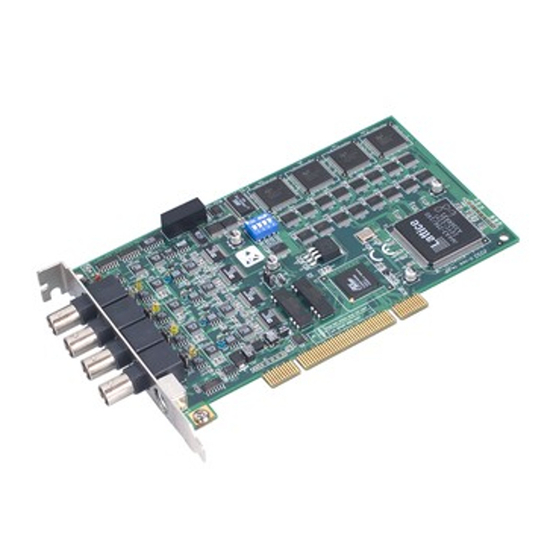
- Page 1 PCI-1714 30 MS/s Simultaneous 4-ch Analog Input Card PCI-1714UL 10 MS/s Simultaneous 4-ch Analog Input Card with Universal PCI User Manual...
- Page 2 No part of this man- ual may be reproduced, copied, translated or transmitted in any form or by any means without the prior written permission of Advantech Co., Ltd. Information provided in this manual is intended to be accurate and reli- able.
- Page 3 Product Warranty (2 years) Advantech warrants to you, the original purchaser, that each of its prod- ucts will be free from defects in materials and workmanship for two years from the date of purchase. This warranty does not apply to any products which have been repaired or...
- Page 4 This product has passed the CE test for environmental specifications when shielded cables are used for external wiring. We recommend the use of shielded cables. This kind of cable is available from Advantech. Please contact your local supplier for ordering information.
-
Page 5: Table Of Contents
Figure 2.6:The Device Name Appearing on the list of De- vices box ............18 Device Testing..............19 Figure 2.7:The Device Test Dialog Box of PCI-1714 . 19 2.5.1 Testing the Analog Input Function ......20 Figure 2.8:Analog Input tab on the Device Test dialog box .............. - Page 6 Internal A/D Sample Clock .......... 33 4.3.2 External A/D Sample Clock 0 ........33 4.3.3 External A/D Sample Clock 1 ........33 Figure 4.5:PCI-1714 Sample Clock Sources ....34 Trigger Sources ............... 34 4.4.1 Software Trigger ............34 4.4.2 External Digital (TTL) Trigger ........34 4.4.3...
- Page 7 Appendix C Register Structure & Format ....... 52 Overview ................ 52 Register Format ............... 52 Table C.1:PCI-1714 register format (Part 1) ....53 Table C.2:PCI-1714 register format (Part 2) ....54 Table C.3:PCI-1714 register format (Part 3) ....55 Table C.4:PCI-1714 register format (Part 4) ....57 A/D Single Value Acquisition.........
- Page 8 PCI-1714 & 1714L User Manual viii...
- Page 9 Introduction This chapter will provide information on the features of the PCI-1714 and PCI-1714UL cards, a quick installation guide, together with some brief infor- mation on software and accessories. Sections include: • Features • Applications • Installation Guide • Software Overview •...
-
Page 10: Chapter 1 Introduction
PCI-1714 and PCI-1714L offer the following main features: • 32-bit PCI bus Mastering DMA data transfer • Four A/D converters for simultaneous sampling • 12-bit A/D converter with up to 30 MS/s for PCI-1714, and 10 MS/s for PCI-1714UL • 4 single-ended analog input channels •... -
Page 11: 32-Bit Pci Bus Mastering Dma Data Transfer
1.1.4 On-board FIFO Memory There is 32k of FIFO sample memory on PCI-1714, and 8k of FIFO sam- ple memory on PCI-1714UL. This is an important feature for faster data transfers and more predictable performance under Windows systems. -
Page 12: Applications
1.2 Applications The following are some of the possible applications of PCI-1714 cards: • Testing Instruments • Ultrasound Imaging • Gamma Camera Imaging • CCD Camera Imaging • Video Digitizing 1.3 Installation Guide Before you install your PCI-1714 or PCI-1714UL card, please make sure you have the following necessary components: •... - Page 13 Figure 1.1: Installation Flow Chart Chapter 1...
-
Page 14: Software Overview
1.4 Software Overview Advantech offers a rich set of DLL drivers, third-party driver supports and application software to help fully utilize the functions of your PCI- 1714 cards: • Device Drivers (on the companion CD-ROM) • LabVIEW driver • ADAQView 1.4.1 Programming Choices for DA&C Cards... -
Page 15: Device Drivers Programming Roadmap
• C++ Builder For instructions on how to begin programming in each development tool, Advantech offers a Tutorial Chapter in the Device Drivers Manual for your reference. Please refer to the corresponding sections in this chapter of the Device Drivers Manual to begin your programming efforts. You can also look at the example source code provided for each programming tool.. -
Page 16: Programming With Device Drivers Function Library
1.5.2 Programming with Device Drivers Function Library Advantech Device Drivers offers a rich function library to be utilized in various application programs. This function library consists of numerous APIs that support many development tools, such as Visual C++, Visual Basic, Delphi and C++ Builder. -
Page 17: Accessories
PCL-1010B-1 is designed for connecting to a signal source. The cable links the PCI-1714 cards with the signal source via the BNC connectors. There are four BNC ports available for simultaneous signal input. - Page 18 PCI-1714 & 1714UL User Manual...
- Page 19 Installation This chapter gives a package item checklist, proper instructions about unpacking and step-by-step procedures for both driver and card installation.. Sections include: • Unpacking • Driver Installation • Hardware Installation • Device Setup & Configuration • Device Testing...
-
Page 20: Chapter 2 Installation
Chapter 2 Installation 2.1 Unpacking After receiving your PCI-1714 package, please inspect its contents first. The package should contain the following items: ! PCI-1714 or PCI-1714UL card ! Companion CD-ROM (DLL driver included) ! User Manual The PCI-1714 cards harbors certain electronic components vulnerable to electrostatic discharge (ESD). -
Page 21: Driver Installation
1714 cards into your system, since this will guarantee a smooth installa- tion process. The Advantech Device Drivers setup program for the PCI-1714 cards is included on the companion CD-ROM that is shipped with your DA&C card package. Please follow the steps below to install the driver software: Step 1: Insert the companion CD-ROM into your CD-ROM drive. - Page 22 Figure 2.2: Different Options for Driver Setup For further information on driver-related issues, an online version of the Device Drivers Manual is available by accessing: Start/Programs/Advantech Automation/Device Driver's Manual PCI-1714 & 1714UL User Manual...
-
Page 23: Hardware Installation
2.3 Hardware Installation After the DLL driver installation is completed, you can now go on to install the PCI-1714 series card in any PCI slot on your computer. It is recommended that you refer to the computer’s user manual or related documentation if you have any doubts. - Page 24 After the PCI-1714 series card is installed, you can verify whether it is properly installed on your system in Device Manager: Access Device Manager through: Start /Control Panel /System /Device Manager. The device name of card should be listed on the Device Manager tab on the System Property Page.
-
Page 25: Device Setup & Configuration
Device Manager is a utility that allows you to setup, configure and test your device, and later store your settings on the system registry. These settings will be used when you call the APIs of Advantech Device Driv- ers. Setting Up and Configuring the Device... - Page 26 Installed Devices as shown below. Figure 2.6: The Device Name Appearing on the list of Devices box Note: As we have noted, the device name “001:<PCI-1714 BoardID=7 I/O=c800H>” begins with a device number “000”, which is specifically assigned to each card. The...
-
Page 27: Device Testing
Figure 2.7: The Device Test Dialog Box of PCI-1714 In the Device Test dialog box, you are free to test various functions of PCI-1714 cards on the analog input tab, functions on the other tabs are not supported for this model. -
Page 28: Testing The Analog Input Function
Scroll the Sampling period scroll bar freely to test any sam- pling rate you want. When the device is fully tested, click the Exit button to end the testing procedure. Figure 2.8: Analog Input tab on the Device Test dialog box PCI-1714 & 1714UL User Manual... - Page 29 Signal Connections This chapter provides useful informa- tion about how to connect input signals to the PCI-1714 cards via the I/O con- nectors. Sections include: • Overview • Switch and Jumper Settings • Signal Connections...
-
Page 30: Chapter 3 Signal Connections
A good signal connection can avoid unnecessary and costly dam- age to your PC and other hardware devices. This chapter provides useful information about how to connect input signals to PCI-1714 cards via the I/O connectors. 3.2 Switch and Jumper Settings PCI-1714 cards have one function switch and five jumper settings. -
Page 31: Boardid Switch Setting (Sw1)
3.2.1 BoardID Switch Setting (SW1) BoardID settings are used to set a board’s unique identifier when multiple identical cards are installed in the same system. PCI-1714UL cards have a built-in DIP switch (SW1), which is used to define each card’s unique identifier. You can determine the unique identi- fier in the register as shown in following table. -
Page 32: Power On Configuration After Hot Reset (Jp1)
3.2.2 Power on Configuration after Hot Reset (JP1) Use JP1 to set the hot reset type of PCI-1714. Power on configuration after hot reset Keep the hardware register setting after hot reset. Load the hardware register default setting after hot reset. (Default setting) 3.2.3 Input Terminator Select (JP2 to JP5) -
Page 33: Signal Connections
3.3 Signal Connections 3.3.1 Pin Assignments The pin assignments for the PS-2 connector and the DB9 connector are shown below. Table 3.1: PS-2 Pin Assignments Description EXT TRIG 0 EXT CLK 0+ EXT CLK 0- EXT CLK 1 Table 3.2: DB9 Pin Assignments Description EXT TRIG 0 EXT CLK 0+... - Page 34 PCI-1714 & 1714UL User Manual...
- Page 35 Operation This chapter describes the following features of the PCI-1714 cards: • Analog input ranges and gains • Analog input acquisition modes • A/D sample clock sources • Trigger sources • Analog Input Data Format...
-
Page 36: Chapter 4 Operation
Each channel on the PCI-1714 cards can measure bipolar analog input signals ranging within ± 5 V FSR, and can be set up with different input ranges respectively. The sampling rate can be up to 30 MS/s for PCI-1714 and 10 MS/s for PCI-1714UL. -
Page 37: Pacer Acquisition Mode
4.2.3 Post-Trigger Acquisition Mode Post-trigger allows you to acquire data based on a trigger event. Posttrig- ger acquisition starts when the PCI-1714 cards detect the trigger event and stop when the preset number of post-trigger samples has been acquired or when you stop the operation. This trigger mode must work with the DMA data transfer mode enabled. -
Page 38: Delay Trigger Acquisition Mode
The delay number of sample ranges from 2 to 65535 as defined in DMA counter. Delay-trigger acquisition starts when the PCI-1714 cards detect the trig- ger event and stop when the specified number of A/D samples has been acquired or when you stop the operation. -
Page 39: About Trigger Acquisition Mode
Once a trigger event happens, the on-going data acquisition will continue until the designated amount of samples have been reached. When the PCI-1714 cards detect the selected about trigger event, the cards keeps acquiring the preset number of samples, and keep the total number of samples on the FIFO. -
Page 40: Pre-Trigger Acquisition Mode
N+2. Figure 4.4: Pre-Trigger Acquisition Mode 4.3 A/D Sample Clock Sources The PCI-1714 cards can adopt both internal and external clock sources for pacer, post-trigger, delay-trigger, about-trigger acquisition modes: • Internal A/D sample clock with 8-bit divider •... -
Page 41: Internal A/D Sample Clock
The external sample clock 0 is a sine wave signal source which is con- verted to a TTL signal inside PCI-1714 cards. This signal is AC coupled. The input impedance of the external clock 0 is 50 ohms and the input level is 5 volts peak-to-peak. -
Page 42: Trigger Sources
4.4.2 External Digital (TTL) Trigger For analog input operations, an external digital trigger event occurs when PCI-1714 cards detect either a rising or falling edge on the External A/D TTL trigger input signal from screw terminal EXT_TRIG on the ADAM- 3909 screw terminal board. -
Page 43: Analog Threshold Trigger
TS0 to TS2 of Write/Read BASE+Eh. On the PCI-1714 cards, the analog trigger threshold voltage level is set using a dedicated 8-bit DAC; you can write or read the flags from AT0 to AT7 on Write/Read BASE+24h to define or identify the analog trigger threshold voltage level. -
Page 44: Analog Input Data Format
Mapping Voltage Hex. Dec. 000h 7FFh 2047d -1 LSB 800h 2048d FFFh 2095d FS-1 LSB 1LSB FS/2048 Table 4.3: Corresponding Full Scale Values for Various Input Volt- age Ranges Gain Range ±5 ±2.5 ±1 ±0.5 PCI-1714 & 1714UL User Manual... - Page 45 Calibration This chapter offers you a brief guide to the calibration procedure. Sections include: • Calibration Procedure...
-
Page 46: Chapter 5 Calibration
Chapter 5 Calibration The PCI-1714 cards have been well calibrated at the factory for initial use. You are not required to calibrate the PCI-1714 cards in normal con- ditions. However, if calibration is required, the procedure shown in the next pages will show how it is done. -
Page 47: Calibration
Step 2:Select the input range of the channel which you want to calibrate. Step 3:Click the Calibration button to start the calibration process. The Calibration Wizard window will pop up. Note: Each calibration process can calibrate only one channel and one input range at a time. Figure 5.2: Click the Calibration Button to Launch the Calibration Step 4:Follow the instruction of Calibration Wizard to input a correct DC voltage as a reference and click the Next button to proceed to the next... - Page 48 Start button is clicked. When the offset calibration is completed, the Status will indicate Succeeded, then click the Next button to proceed to the next step Figure 5.5: Offset Calibration Succeeded PCI-1714 & 1714UL User Manual...
- Page 49 Step 6a:Once the Status indicates Failed, please check if both the wiring and the input voltage are correct. When finished checking, click the Start button again to restart the procedure, or click the Cancel button to stop the calibration. Figure 5.6: Offset Calibration Failed Step 7:If the offset calibration is completed, it will proceed to the Gain Calibration.
- Page 50 Unknown as default at the beginning. Figure 5.8: The Adjustment Process of Gain Calibration Step 9:When the gain calibration is completed click the Next button to proceed. Figure 5.9: Gain Calibration Succeeded PCI-1714 & 1714UL User Manual...
- Page 51 Step 9a:Once the Status indicates Failed, please check if both the wiring and the input voltage are correct. When finished checking, click the Start button again to restart the procedure, or click the Cancel button to stop the calibration. Figure 5.10: Gain Calibration Failed Step 10:When the current channel is calibrated, click the Finish button to end the procedure.
- Page 52 PCI-1714 & 1714UL User Manual...
- Page 53 Specifications...
-
Page 54: Appendix A Specifications
+5 V @ 1 A ; +12 V @ 700mA Max. 0~70° C (32~158° F) Temperature Operating -20 ~ 85° C (-4 ~ 185° F) Storage 5~95%RH, non-condensing (refer to IEC 68-2-3) Relative Humidity CE certified Certification PCI-1714 & 1714UL User Manual... -
Page 55: Pci-1714Ul Analog Input
Range By analog input range Trigger Input Resolution 8-bit Frequency Up to 1MHz PCI-1714: 30 MHz is only for FIFO depth of 32K. PCI-1714UL: 10 MHz is only for FIFO depth of 8K. Continuous acquisition depends on performance. Appendix A... - Page 56 PCI-1714 & 1714UL User Manual...
- Page 57 Block Diagram...
-
Page 58: Appendix B Block Diagram
Appendix B Block Diagram PCI-1714 & 1714UL User Manual... - Page 59 Register Structure & Format...
-
Page 60: Appendix C Register Structure & Format
PCI-1714 cards are delivered with an easy-to-use 32-bit DLL driver for user programming under the Windows 98, 2000, and XP operating sys- tems. We advise users to program the PCI-1714 using the 32-bit DLL driver provided by Advantech to avoid the complexity of low-level pro- gramming by register. - Page 61 Table C-1 shows the function of each register of the PCI-1714 cards or driver and their address relative to the cards’ base address. Table C.1: PCI-1714 register format (Part 1) Base PCI-1714 Register Format Address + HEX 13 12 11 10 9...
- Page 62 Table C.1: PCI-1714 register format (Part 1) Ch W Clock Source and Divider Register Eh W Trigger Mode and Source Register TRGF DMA TSE TS2 TS1 TS0 TM2 TM1 TM0 _TCF TRGF DMA TSE TS2 TS1 TS0 TM2 TM1 TM0 _TCF Table C.2: PCI-1714 register format (Part 2)
- Page 63 Table C.2: PCI-1714 register format (Part 2) 18h W FIFO 2 Programmable Flag Register PF9 PF8 PF PF5 PF4 PF3 PF2 PF1 R FIFO 2 Programmable Flag Register PF9 PF8 PF PF5 PF4 PF3 PF2 PF1 1Ah W FIFO 3 Programmable Flag Register...
- Page 64 Table C.3: PCI-1714 register format (Part 3) 24h W Analog Trigger Threshold voltage Register AT2 AT1 AT0 R Analog Trigger Threshold voltage Register AT2 AT1 AT0 26h W N/A R N/A 28h W Calibration Command Register CG1 CG0 X CD2 CD1 CD0...
-
Page 65: A/D Single Value Acquisition
Table C.4: PCI-1714 register format (Part 4) Base PCI-1714 Register Format Address + HEX 30h W Reset start read channel to CH0 R AD Channel n DATA OV G1 G0 AD1 AD9 AD8 AD7 AD6 AD5 AD4 AD3 AD2 AD1 AD0... - Page 66 This bit indicates whether the input voltage is over range or not. Read 1 means over range. TRGF Trigger Flag (For about trigger use only) The trigger flag indicates whether a trigger event has happened during A/ D conversion process. PCI-1714 & 1714UL User Manual...
-
Page 67: Ai Range Control- Write/Read Base+8
C.4 AI Range Control- Write/Read BASE+8 Table C.6: Register for Analog Input Range Control Base PCI-1714 Register Format Address + HEX 15 14 12 11 10 9 8 7 AI Range Control Register CH0_ CH0_ Analog Input Range Selector These registers are used to select the analog input range for each channel. -
Page 68: Clock Source And Divider- Write/Read Base+C
255 divide by 256 CKS1: CKS0 Clock Source selector These 2 bits select the clock source feed to the A/D converters. CKS1 CKS0 Clock source Internal clock 60MHz External clock 0 External clock 1 PCI-1714 & 1714UL User Manual... -
Page 69: Trigger Mode And Source- Write/Read Base+E
TSE TS2 TS1 TS0 TM2 TM1 TM0 TM2: TM0 Trigger Mode selector There are 5 trigger modes for PCI-1714 cards. Please refer to the opera- tion theorem for more information. Meaning Single value acquisition mode (SW trigger) Pacer acquisition mode... -
Page 70: Fifo Control- Write Base+10,12
Write 1 to this bit to clear FIFO data. FRSTn (n = 0~3) FIFO Reset register Write 1 to this bit to clear FIFO data and reset the AE and AF flag posi- tion to 7FH. PCI-1714 & 1714UL User Manual... -
Page 71: Fifo Status- Read Base+10,12
C.9 FIFO Status- Read BASE+10,12 Table C.11: Register for FIFO Status Base PCI-1714 Register Format Address + HEX 15 14 13 11 10 7 6 5 10h R FIFO Status Register FIFO FIFO FIFO FIFO1 FIFO FIFO FIFO FIFO0 FIFO... -
Page 72: Fifo For Programmable Flag - Write/Read
PF14: PF0 FIFO n Programmable Flag Register (n = 0 ~3) The FIFO on PCI-1714 cards is very powerful. It allows user to define the indicate flag in any depth. There are two flags could be defined: FIFO Almost Empty flag and FIFO Almost Full flag. To define these flags must follow the procedure: First write is the Almost Empty flag offset count from the empty. -
Page 73: Dmacounter-Write/Read Base+1C, Write Base+1E
C.11 DMA Counter - Write/Read BASE+1C, Write BASE+1E Table C.13: Register for DMA Counter Base PCI-1714 Register Format Address + HEX 15 14 13 12 11 10 9 1Ch W DMA Counter Register CN9 CN8 CN7 CN6 CN5 CN4 CN3 CN2 CN1 CN0... -
Page 74: Interrupt Control/Flag- Write/Read Base+20
R Interrupt Flag INTF3 INTF2 INTF1 INTF0 C.12.1 Interrupt Control Register PCI-1714 cards provide 9 sources to generate the interrupt. Write 1 to enable the interrupt, write 0 to disable. The INTE is control the total inter- rupt. FIFO0_HFFIFO 0 Half Full... -
Page 75: Interrupt Flag
INTF Total Interrupt flag C.13 Clear Interrupt- Write BASE+22 Table C.15: Register for Clear Interrupt Base PCI-1714 Register Format Address + HEX Clear Interrupt Clear Interrupt Write any value to this address will clear interrupt. It will clear all flags to 0 if there is no any interrupt in coming. -
Page 76: Analog Trigger Threshold V-Write/Read Base+24
These registers set the analog trigger threshold voltage level. AT7: AT0 ±0.5V ±1V ±2.5V ±5V 0.496 0.992 2.48 4.96 0.492 0.984 2.46 4.92 0.004 0.008 0.02 0.04 -0.004 -0.008 -0.02 -0.04 -0.496 -0.992 -2.48 -4.96 -0.5 -2.5 PCI-1714 & 1714UL User Manual... -
Page 77: Calibration Command- Write/Read Base+28
C.15 Calibration Command- Write/Read BASE+28 Table C.17: Register for Calibration Command Base PCI-1714 Register Format Address + HEX 15 14 13 28h W Calibration Command Register CG1 CG0 X CM2 CM1 CM0 CD CD3 CD2 CD1 CD0 CG1 CG0 CBU... -
Page 78: Boardid- Read Base+2C
Reset DMA start channel to CH0 Write any value to BASE+30h to reset DMA transfer data from CH0. Before start DMA transfer, user has to reset the start channel to CH0. This only for four channels DMA data transfer. PCI-1714 & 1714UL User Manual... -
Page 79: Ad Channel N Data- Read Base+30,32
C.18 AD Channel n DATA- Read BASE+30,32 Table C.20: Register for AD Channel n DATA Base PCI-1714 Register Format Address + HEX 14 13 12 11 30h R AD Channel n DATA TRGF OV G1 G0 AD11 AD10 AD9 AD8 AD7 AD6 AD5 AD4 AD3 AD2 AD1 AD0... -
Page 80: Dma Request Selector- Write Base+34
34h W DMA Request selector DMA Request selector This bit select the DMA request (hardware signal DREQ), user could use FIFO 0 flag or FIFO 2 flag to generate DREQ. FIFO 0 flag FIFO 2 flag PCI-1714 & 1714UL User Manual...
Need help?
Do you have a question about the PCI-1714 and is the answer not in the manual?
Questions and answers