Table of Contents
Advertisement
Quick Links
Advertisement
Table of Contents

Related Manuals for Advantech PCI-1718 Series


Summary of Contents for Advantech PCI-1718 Series
- Page 1 PCI-1718 Series 12-bit Multifunction Cards with Universal PCI Bus User Manual...
- Page 2 No part of this man- ual may be reproduced, copied, translated or transmitted in any form or by any means without the prior written permission of Advantech Co., Ltd. Information provided in this manual is intended to be accurate and reli- able.
- Page 3 Product Warranty (2 years) Advantech warrants to you, the original purchaser, that each of its prod- ucts will be free from defects in materials and workmanship for two years from the date of purchase. This warranty does not apply to any products which have been repaired or...
- Page 4 This product has passed the CE test for environmental specifications when shielded cables are used for external wiring. We recommend the use of shielded cables. This kind of cable is available from Advantech. Please contact your local supplier for ordering information.
-
Page 5: Table Of Contents
Accessories..............10 Chapter 2 Installation ............. 12 Unpacking ............... 12 Driver Installation ............13 Figure 2.1:Setup Screen of Advantech Automation Soft- ware 14 Figure 2.2:Different Options for Driver Setup .... 14 Hardware Installation ............15 Device Setup & Configuration ........16 Figure 2.3:The Device Manager Dialog Box .... - Page 6 Digital I/O Registers - BASE + 03/0BH ......68 Table C.9:Register for Digital Output ......68 Table C.10:Register for Digital Output ...... 69 D/A Output — BASE+04/05H ........69 Table C.11:Register for D/A Output ......69 C.10 FIFO Interrupt Control — BASE+06H......70 PCI-1718 Series User Manual...
- Page 7 Table C.12:Register for FIFO Interrupt Control ..70 C.11 Clear Interrupt Request — BASE+08H ......71 Table C.13:Register for Clear Interrupt Request ..71 C.12 A/D Status — BASE+08H..........71 Table C.14:Register for A/D Status ......71 C.13 A/D Control — BASE+09H ........... 73 Table C.15:Register for A/D Control ......
- Page 8 PCI-1718 Series User Manual viii...
- Page 9 Introduction This chapter introduces the PCI-1718 cards and their typical applications. Sections include: • Features • Applications • Installation Guide • Software Overview • Device Driver Programming Road- • Accessories...
-
Page 10: Chapter 1 Introduction
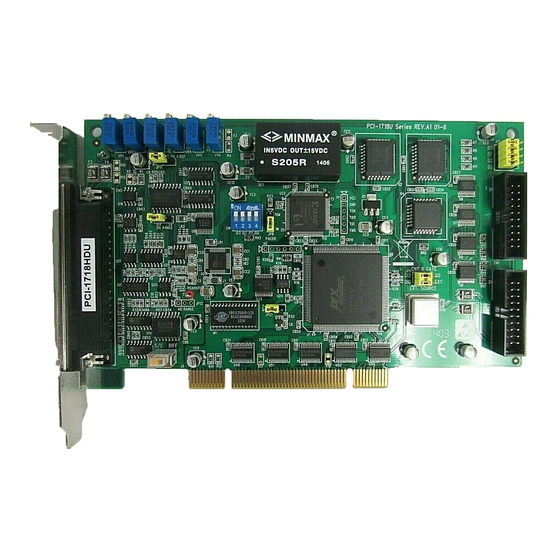
Chapter 1 Introduction Thank you for buying the Advantech PCI-1718HDU/HGU. PCI- 1718HDU/HGU is a PCI-Bus multifunction card for IBM PC/XT/AT or compatible computers. It offers the five most desired measurement and control functions: • 12-bit A/D conversion • D/A conversion •... -
Page 11: Features
1.1 Features • Register level programming compatible with PCL-818HD/HG • 16 single-ended or 8 differential A/D inputs, switch selectable • 12-bit A/D converter, up to 100 kHz sampling rate • Programmable gain for each input channel • Automatic Channel/Gain Scanning •... -
Page 12: Applications
Note: For detailed specifications of the PCI- 1718HDU/HGU, please refer to Appendix A. 1.2 Applications • Transducer and sensor measurements • Waveform acquisition and analysis • Process control and monitoring • Vibration and transient analysis PCI-1718 Series User Manual... -
Page 13: Installation Guide
Before you install your PCI-1718HDU/HGU card, please make sure you have the following necessary components: • PCI-1718HDU/HGU DA&C card • PCI-1718HDU/HGU User Manual • Driver software Advantech DLL drivers (included in the companion CD-ROM) • Personal computer or workstation with a PCI-bus slot (running Win- dows 98/2000/XP) •... -
Page 14: Figure 1.1:Installation Flow Chart
Figure 1.1: Installation Flow Chart PCI-1718 Series User Manual... -
Page 15: Software Overview
Device Drivers Advantech Device Driver software is included on the companion CD- ROM at no extra charge. It also comes with all Advantech DA&C cards. Advantech’s Device Drivers features a complete I/O function library to help boost your application performance. Advantech Device Drivers for Windows 98/2000/XP works seamlessly with development tools such as Visual C++, Visual Basic, Borland C++ Builder and Borland Delphi. -
Page 16: Device Driver Programming Roadmap
• C++ Builder For instructions on how to begin programming works in each develop- ment tool, Advantech offers a Tutorial Chapter in the Device Drivers Manual for your reference. Please refer to the corresponding sections in this chapter on the Device Drivers Manual to begin your programming efforts. - Page 17 Programming with Device Drivers Function Library Advantech Device Drivers offer a rich function library that can be uti- lized in various application programs. This function library consists of numerous APIs that support many development tools, such as Visual C++, Visual Basic, Delphi and C++ Builder.
-
Page 18: Accessories
1.6 Accessories Advantech offers a complete set of accessory products to support the PCI-1718HDU/HGU card. These accessories include: Wiring Cables PCL-10120 The PCL-10120 cable is a 20-pin flat cable for PCI-1718HDU/HGU cards. PCL-10137 The PCL-10137 shielded cable is specially designed for PCI-1718HDU/ HGU cards to provide high resistance to noise. - Page 19 Installation This chapter provides a packaged item checklist, proper instructions for unpacking and step-by-step procedures for both driver and card installation.. Sections include: • Unpacking • Driver Installation • Hardware Installation • Device Setup & Configuration...
-
Page 20: Chapter 2 Installation
• Avoid physical contact with materials that could hold static electricity such as plastic, vinyl and Styrofoam. • Whenever you handle the card, grasp it only by its edges. DO NOT TOUCH the exposed metal pins of the connector or the electronic com- ponents. PCI-1718 Series User Manual... -
Page 21: Driver Installation
1718HDU/HGU card into your system, since this will guarantee a smooth installation process. The Advantech Device Drivers Setup program for the PCI-1718HDU/ HGU card is included in the companion CD-ROM that is shipped with your DA&C card package. Please follow the steps below to install the driver software: Insert the companion CD-ROM into your CD-ROM drive. -
Page 22: Figure 2.1:Setup Screen Of Advantech Automation Soft Ware
Figure 2.1: Setup Screen of Advantech Automation Software Select the Device Drivers option. Select the specific device then just follow the installation instruc- tions step by step to complete your device driver installation and setup. Figure 2.2: Different Options for Driver Setup... -
Page 23: Hardware Installation
Plug in the power cord and turn on the computer. After your card is properly installed on your system, you can now config- ure your device using the Advantech Device Manager Program that has itself already been installed on your system during driver setup. A com- plete device installation procedure should include device setup, configu- ration and testing. -
Page 24: Device Setup & Configuration
2.4 Device Setup & Configuration The Advantech Device Manager program is a utility that allows you to set up, configure and test your device, and later stores your settings on the system registry. These settings will be used when you call the APIs of Advantech Device Drivers. -
Page 25: Figure 2.4:The Device Setting Dialog Box
Configuring the Device On the Device Setting dialog box (Fig. 2-4), you can configure the A/D channels configuration either as 8 Differential or 16 Single- ended, and specify the D/A voltage reference either as External or Internal. Figure 2.4: The Device Setting Dialog Box After you have finished configuring the device, click OK and the device name will appear in the Installed Devices box as seen below: Figure 2.5: Device Name Appearing on the List of Devices Box... -
Page 26: Figure 2.6:The Test Utility Dialog Box
Figure 2.6: The Test Utility Dialog Box For more detailed information, please refer to Chapter 2 of the Device Drivers Manual. You can also find rich examples on the CD-ROM to speed up your pro- gramming. PCI-1718 Series User Manual... -
Page 27: Signal Connections
Signal Connections This chapter provides useful informa- tion about how to connect input and output signals to the PCI-1718 cards via the I/O connector.. Sections include: • Overview • Switch and Jumper Settings • Signal Connections • Field Wiring Considerations... -
Page 28: Chapter 3 Signal Connections
Trigger Source & Gate Control S.E/Diff Connection Setting Setting Timer Clock Setting IDE 20-pin Header 1 JP10 Internal Reference Voltage Set- IDE 20-pin Header 2 ting Jp11 D/A Reference Voltage Setting DB-37 Pin Connector JP21 Reset Protection Setting PCI-1718 Series User Manual... -
Page 29: Setting The Boardid Switch (Sw1)
3.2.1 Setting the BoardID Switch (SW1) BoardID settings are used to set a board’s unique identifier when multiple identical cards are installed in the same system. PCI-1718 cards have a built-in DIP switch (SW1), which is used to define each card’s unique identifier. You can determine the unique identifier in the register as shown in Table 3.1. -
Page 30: Channel Configuration, S/E Or Diff (Sw2)
Jumper JP10 selects either -5 V or -10 V onboard reference voltage. With JP11 set to INT the D/A chan- nel has an output range of 0 to +5 V or 0 to +10 V, respectively. PCI-1718 Series User Manual... -
Page 31: Internal Voltage Reference, -10 V Or -5 V (Jp10)
When you set JP11 to EXT, the D/A converter takes its reference voltage input from pin 31 of connector CN3. You can apply any voltage between -10 V and +10 V to this pin to function as the external reference. The ref- erence input can be either DC or AC (<100 kHz). -
Page 32: Timer Clock Selection (Jp8)
Fclk is 1 MHz or 10 MHz, as set by jumper JP8. Div 1 and Div2 are the dividers set in counter 1 and counter 2 in the 8254. Table 3.5: Summary of Jumper JP8 Settings Jumper Function description 1 MHz (default) 10 MHz PCI-1718 Series User Manual... -
Page 33: Ext. Trigger And Counter Gate 0 Control (Jp5)
3.2.6 Ext. trigger and Counter Gate 0 Control (JP5) Jumper 5 determines the source of A/D external trigger signal (Lower) and gate control for counter 0 on 8254 timer/counter.(Upper). Table 3.6: Summary of Jumper Settings Jumper Function description G0 (default) (Upper) Ext. -
Page 34: Table 3.7:Summary Of Jumper Settings
Table 3.7: Summary of Jumper Settings Jumper Function Description JP1 (first) D0 (default) JP1 (sec- ond) D1 (default) JP1 (third) D2 (default) (fourth) D3 (default) PCI-1718 Series User Manual... -
Page 35: Setting The Time To Reset Digital Outputs
3.2.8 Setting the Time to Reset Digital Outputs Some users will want the capability of clearing each digital output when the system (or PC) issues a reset signal on the PCI bus. Other users will want to clear their signal outputs only as part of system power-on. PCI-1718 cards satisfy both these needs with jumper JP21. -
Page 36: Signal Connections
Counter 0 OUT 18 37 PACER Counter 0 OUT 18 37 PACER +5 V +5 V Figure 3.2: I/O Connector Pin Assignments for the PCI-1718 Series Note: S0/S1 is NC, and S2/S3 is AGND for PCI-1718HGU PCI-1718 Series User Manual... -
Page 37: I/O Connector Signal Description
3.3.1 I/O Connector Signal Description Table 3.9: I/O Connector Signal Descriptions Signal Reference Direction Description Name A/D S Analog input (single-ended), channels 0 A.GND Input <0..15> through 15. A/D H Analog input high (differential), channels A.GND Input <0..7> 0 through 7. A/D L Analog input low (differential), channels A.GND... -
Page 38: Analog Input Connections
"floating" source. A connection must exist between LOW and ground to define a common reference point for floating signal sources. To measure a floating sources connect the input channels as shown below: HIGH A.GND PCI-1718 Series User Manual... - Page 39 If the signal source has one side connected to a local ground, the signal source ground and the PCI-1718HDU/HGU ground will not be at exactly the same voltage, as they are connected through the ground return of the equipment and building wiring. The difference between the ground volt- ages forms a common-mode voltage.
- Page 40 It provides 20-pin flat cable and DB-37 cable connectors. It also includes CJC (Cold Junction Compensation) circuits. Special circuit pads on the PCLD-8115 accommodate passive signal con- ditioning components. You can easily implement a low-pass filter, atten- uator or current shunt by adding resistors and capacitors. PCI-1718 Series User Manual...
-
Page 41: Figure 3.3:Analog Output Connections
Analog Output Connection The PCI-1718HDU/HGU provides one D/A output channel. You can use the internal precision -5 V or -10 V reference to generate 0 to +5 V or 0 to +10 V D/A output. Use an external reference for other D/A output ranges. The maximum reference input voltage is ±10 V and maximum output scaling is ±10 V. -
Page 42: Digital Signal Connections
To receive an OPEN/SHORT signal from a switch or relay, add a pull-up resistor to ensure that the input is held at a high level when the contacts are open. See the figure below: 4.7K D.GND PCI-1718 Series User Manual... -
Page 43: Field Wiring Considerations
3.4 Field Wiring Considerations When you use PCI-1718 cards to acquire data from outside, noises in the environment might significantly affect the accuracy of your measure- ments if due cautions are not taken. The following measures will be help- ful to reduce possible interference running signal wires between signal sources and the PCI-1718 card. - Page 44 PCI-1718 Series User Manual...
- Page 45 Programming Guide This chapter provides useful informa- tion about how to do register level pro- gramming for PCI-1718 cards. Sections include: • Overview • Programming with the Driver • Register Programming • Programming with LabVIEW and ActiveDAQ...
-
Page 46: Chapter 4 Programming Guide
PCL-818 series so you can easily use older applications of the PCL- 818 series with PCI-1718 cards.We also advise users to program the PCI- 1718 cards using the 32-bit Device Drivers provided by Advantech to avoid the complexity of low- level registry programming. -
Page 47: Software Trigger And Polling
4.3.1 Software Trigger and Polling Set Scan Channel w Base+0 2H MUX Scan w Base+0 1H Channel Control & A/D Range Control Set Software w Base+ 09H Trigger and Disable Generated Interrupt Software A/D w Base+ 00H Trigger EOC!=0 Check EOC r Base+ 08H EOC=0 Get Data... - Page 48 //Set Channel 0 outportb(base_addr+0x01,0x00); //Set A/D range outportb(base_addr+0x02,0x11); //Set Channel 1 outportb(base_addr+0x01,0x01); //Set A/D range outportb(base_addr+0x02,0x10); //Scan Channel 0-1 outportb(base_addr+0x09,0x00); while(i<AD_NO){ outportb(base_addr+0x00,0); //Software Trigger do {eoc=inportb(base_addr+0x08); eoc=eoc&0x01;//Get EOC} while(eoc!=0); //Check EOC ad_lb=inportb(base_addr+0x00);// A/D LowByte ad_hb=inportb(base_addr+0x01);// A/D HighByte i++; PCI-1718 Series User Manual...
-
Page 49: Pacer Trigger Mode With Interrupt
4.3.2 Pacer Trigger Mode with Interrupt Set to Software Trigger Mode To w Base+ 09H Disable Trigger. r Base+ 00H Get Data r Base+01H Clear Device MUX Scan Interrupt Request Channel Control & w Base+0 2H w Base+0 1H A/D Range Control Clear System w Base+ 08H... - Page 50 //Declaration int i=1; /****** Access your base address ******/ Add you code here /*******************************************/ outportb(base_addr+9,0x00); //Set Software Trigger and Disable INT. outportb(base_addr+2,0x00); //Mux Scan Channel Control outportb(base_addr+1,0x00); //A/D Range Control PCI-1718 Series User Manual...
- Page 51 /***** Set Pacer *****/ outportb(base_addr+0x0f,0x7E); //Pacer=1M/clk1/clk2 outportb(base_addr+0x0d,0x0A); //clk1 outportb(base_addr+0x0d,0x00); //10=0x0A ; 100=0x64 ; 1000=0x3E8 outportb(base_addr+0x0f,0xBE); outportb(base_addr+0x0e,0x0A); //clk2 outportb(base_addr+0x0e,0x00); /***** Pacer=1M/10/10=10k ******/ /***** Set ISR *****/ Add you code here /********************/ /***** Set Interrupt *****/ Add you code here /********************/ outportb(base_addr+8,0); //Clear Interrupt outportb(base_addr+9,0xf3);...
- Page 52 /***** Add code on here *****/ iflag = 1; //Interrupt Flag outportb(base_addr+0x08,0);// Clear Interrupt /****************************/ outportb(0x20,0x20); outportb(0xA0,0x20); enable(); PCI-1718 Series User Manual...
-
Page 53: Pacer Trigger Mode With Interrupt And Fifo
4.3.3 Pacer Trigger Mode with Interrupt and FIFO Set To Software Trigger Mode To w Base+ 09H Start ISR Disable Trigger Get 512 r Base+ 17H MUX Scan Samples data r Base+18H w Base+0 2H Channel Control & (Half-Full of FIFO) A/D Range w Base+0 1H Control... - Page 54 #define AD_NO 4096; int iflag; int base_addr; void main(void) int ad_lb,ad_hb; int i=1; int k=0; //FIFO index /****** Access your base address ******/ Add you code here /*******************************************/ // Set Software Trigger and Disable Nor INT outportb(base_addr+0x09,0x00); PCI-1718 Series User Manual...
- Page 55 outportb(base_addr+0x02,0x00); //MUX Scan Channel Control outportb(base_addr+0x01,0x03); //Channel 1 Gain Setting outportb(base_addr+0x02,0x11); // MUX Scan Channel Control outportb(base_addr+0x01,0x08); // Channel 2 Gain Setting outportb(base_addr+0x02,0x10); //Scan Channel 0-1 /***** Set Pacer *****/ outportb(base_addr+0x0f,0x7e); outportb(base_addr+0x0d,10); //Divide By 1 outportb(base_addr+0x0d,0); outportb(base_addr+0x0f,0xbe); outportb(base_addr+0x0e,20); //Divide By 2 outportb(base_addr+0x0e,0);...
- Page 56 /***** Save to Memory *****/ Add your code here /**************************/ i++; /*******************************************/ void interrupt isr(void) disable(); iflag = 1; /***** Add your code here *****/ outportb(base_addr+0x14,0); // Clear FIFO Interrupt /******************************/ outportb(0x20,0x20); outportb(0xA0,0x20); enable(); PCI-1718 Series User Manual...
-
Page 57: Programming With Labview And Activedaq
4.4 Programming with LabVIEW and ActiveDAQ Advantech offers not only a rich set of DLL drivers, but also third-party driver support and application software to help fully exploit the functions of your PCI-1718 cards. For more detailed information for these... - Page 58 PCI-1718 Series User Manual...
- Page 59 Specifications...
-
Page 60: Appendix A Specifications
(1LSB) (1LSB) DNLE: ±1LSB PCI-1718HDU Accuracy INLE: ±1LSB Offset error: Adjustable to 0 THD: -80 dB ENOB: 11 bits Range 0~10 0~2.5 0~1.25 Zero Drift ( µV/°C) Range ±10 ±5 ±2.5 ±1.25 ±0.625 Gain Drift (PPM/°C) PCI-1718 Series User Manual... -
Page 61: Analog Output
±11 V max. (operational) Common Mode Voltage ±15 V Max. Input Voltage 30 Vp-p Input Protect 100 MΩ/10pF(Off); 100 MΩ/100pF(On) Input Impedance Software, on-board Programmable Pacer or External Trigger Mode 0.8 V max. External TTL Trigger Input High 2.0 V min. A.2 Analog Output Channels 12-bit... -
Page 62: Digital Input
Input Channels 0.4V max. Input Voltage High 2.4 V min. 0.4 V max.@ -0.2mA Input Load High 2.7 V min.@20µA A.4 Digital Output Output Channels 0.4 V max.@ +8.0mA (sink) Output Voltage High 2.4 V min.@ -0.4mA(source) PCI-1718 Series User Manual... -
Page 63: Counter/Timer
A.5 Counter/Timer 82C54 or equivalent Counter chip 3 channels, 2 channels are permanently configured as Channels programmable pacers; 1 channel is free for user appli- cation 16-bit Resolution TTL level Compatibility Channel 1: 10 MHz Base Clock Channel 2: Takes input from output of channel 1 Channel 0: Internal 100 kHz or external clock (10 MHz max.) selected by software 10 MHz... -
Page 64: General
Max. 0~60° C (32~158° F) Temperature Operating (refer to IEC 68-2-1,2) -20~ 70° C (-4~158° F) Storage 5~85%RH non-condensing Relative Humidity Operating (refer to IEC 68-1,-2,-3) 5~95%RH non-condensing Storage (refer to IEC 68-1,-2,-3) CE certified Certifications PCI-1718 Series User Manual... - Page 65 Block Diagrams...
-
Page 66: Appendix B Block Diagrams
Appendix B Block Diagrams PCI-1718 Series User Manual... - Page 67 Register Structure & Format...
-
Page 68: Appendix C Register Structure & Format
Windows 98/2000/XP operating sys- tems. We advise users to program the PCI-1718 cards using the 32-bit Device Drivers provided by Advantech to avoid the complexity of low- level registry programming. The most important consideration in programming the PCI-1718 cards at the register level is to understand the function of the cards’... - Page 69 Table C.1: PCI-1718HDU/HGU Register Format (Part 1) Base Addr. +HEX A/D low byte data and channels Software A/D trigger A/D high byte data and channels AD11 AD10 A/D range control MUX scan channel status CC3 CC2 CC1 CC0 MUX scan channel control CH1 CH0 Digital Input (low byte) Digital Output (low byte)
- Page 70 Digital Input (high byte) DI15 DI14 DI13 DI12 DI11 DI10 Digital Output (high byte) DO15 DO14 DO13 DO12 DO11 DO10 DO9 DO8 Counter 0 Counter 0 Counter 1 Counter 1 Counter 2 Counter 2 Counter Control PCI-1718 Series User Manual...
- Page 71 Table C.3: PCI-1718HDU/HGU Register Format (Part 3) Base Addr. +HEX BoardID Clear FIFO Interrupt Request A/D data and channels from FIFO A/D data and channels from FIFO AD11 AD10 AD9 FIFO status FIFO clear Appendix C...
-
Page 72: A/D Data And Channels - Base+00H~01H
Bits 1 and 0 of register BASE+09H select the trigger source. See page 67 for BASE+09H register layout and programming information. Table C.5: Register for Software A/D Trigger Write Software A/D trigger Bit # BASE + 00H PCI-1718 Series User Manual... -
Page 73: A/D Range Control - Base+01H
C.5 A/D Range Control — BASE+01H Each A/D channel has its own individual input range, controlled by a range code stored in onboard RAM. If you want to change the range code for a given channel, select the channel as the start channel in register BASE+02H, MUX scan (described in the next section), then write the range code to bits 0 to 3 of BASE+01H. - Page 74 PCI-1718HGU Gain Code Input Range (V) Unipolar/Bipolar ±5V ±0.5V ±0.05V ±0.005V 0 to 10V 0 to 1V 0 to 0.1V 0 to 0.01V ±10V ±1V ±0.1V ±0.01V Note: G3 and G2 are not used for PCL-818L PCI-1718 Series User Manual...
-
Page 75: Mux Scan Channel Control - Base+02H
C.6 MUX Scan Channel Control — BASE+02H The write register at BASE+02H controls multiplexer (MUX) scanning. The high nibble provides the stop scan channel number, and the low nib- ble provides the start scan channel number. Writing to this register auto- matically initializes the MUX to the start channel. -
Page 76: Mux Scan Channel Status - Base+02H
DO6 DO5 DO4 DO3 DO2 DO1 DO0 BASE + 0BH DO15 DO14 DO13 DO12 DO11 DO10 DO9 DO8 DO15 ~ DO0 Digital output data The least significant bit (LSB) of the DO data DO15 The most significant bit (MSB) PCI-1718 Series User Manual... -
Page 77: D/A Output - Base+04/05H
Table C.10: Register for Digital Output Read Digital Input Bit # BASE + 03H BASE + 0BH DI15 DI14 DI13 DI12 DI11 DI10 DI15 ~ DI0 Digital input data The least significant bit (LSB) of the DI data DI15 The most significant bit (MSB) Note: Digital Outputs D0 - D3 is selectable from the 20-pin connector or the 37-pin D connector. -
Page 78: Fifo Interrupt Control - Base+06H
D/A signal connections. C.10 FIFO Interrupt Control — BASE+06H Table C.12: Register for FIFO Interrupt Control Write FIFO interrupt control Bit # BASE + 06H AD12_16 FINT FINT Enable/disable FIFO interrupt FIFO interrupt disabled FIFO interrupt enabled PCI-1718 Series User Manual... -
Page 79: Clear Interrupt Request - Base+08H
C.11 Clear Interrupt Request — BASE+08H Write any value to register BASE+08H to clear the interrupt request. Table C.13: Register for Clear Interrupt Request Write A/D control Bit # BASE + 09H C.12 A/D Status — BASE+08H Read-only register BASE+08H provides information on the A/D configu- ration and operation. - Page 80 Your software should therefore wait for the signal SNT = 1 before it reads the conversion data. It should then clear the INT bit by writing any value to the A/D status register BASE+08H. PCI-1718 Series User Manual...
-
Page 81: A/D Control - Base+09H
C.13 A/D Control — BASE+09H Read/write register BASE+09H provides information on the PCI- 1718HDU/HGU's operating modes. Table C.15: Register for A/D Control Read/Write A/D control Bit # BASE + 09H INTE INTE Disable/enable generated interrupts Disables the generation of interrupts. No interrupt signal can be sent to the PC bus. -
Page 82: Timer/Counter Enable - Base+0Ah
Connects Counter 0 internally to a 100 KHz clock source C.15 Programmable Timer/Counter — BASE+0C~0FH The four registers located at addresses BASE+0CH, BASE+0DH, BASE+0EH and BASE+0FH are used for the Intel 8254 programmable timer/counter. Please refer to the 8254 product literature for detailed application information. PCI-1718 Series User Manual... -
Page 83: Clear Fifo Interrupt Request - Base+14H
C.16 Clear FIFO Interrupt Request — BASE+14H Write any value to this I/O port to clear the FIFO's interrupt request. Table C.17: Register for Clear FIFO Interrupt Request Write Clear FIFO Interrupt Request Bit # BASE + 14H X C.17 A/D Data and Channel from FIFO - BASE + 17/18H The PCL-818HD/HG stores data from A/D conversions in a 1 K word First-In First-Out (FIFO) data buffer. -
Page 84: Fifo
C.19 FIFO Clear — BASE+19H Writing any value to BASE+19H clears all data in the FIFO and sets the empty flag (EF) to 1. Table C.20: Register for FIFO Clear Write FIFO clear Bit # BASE + 19H X PCI-1718 Series User Manual... -
Page 85: Register Programming Flow Chart
C.20 Register Programming Flow Chart C.20.1 Software Trigger Mode with Polling Set Scan Channel w Base+0 2H MUX Scan w Base+0 1H Channel Control & A/D Range Control Set Software w Base+ 09H Trigger and Disable Generated Interrupt Software A/D w Base+ 00H Trigger EOC!=0... -
Page 86: Pacer Trigger Mode With Interrupt
Base+ 08H Disable Generated Interrupt Request Interrupt Clear System Interrupt Request Disable System To Accept w Base+0 9H Interrupt Set To Pacer Trigger Mode To w Base+ 09H Enable Trigger System Ready For Data Acquisition Interrupt PCI-1718 Series User Manual... -
Page 87: Pacer Trigger Mode With Interrupt [Fifo Used]
C.20.3 Pacer Trigger Mode with Interrupt [FIFO Used] Set To Software Trigger Mode To w Base+ 09H Start ISR Disable Trigger Get 512 r Base+ 17H MUX Scan Samples data r Base+18H w Base+0 2H Channel Control & (Half-Full of FIFO) A/D Range w Base+0 1H Control... - Page 88 PCI-1718 Series User Manual...
- Page 89 Calibration This appendix provides brief informa- tion on PCI-1718 card calibration. Reg- ular calibration checks are important to maintain accuracy in data acquisition and control applications.
-
Page 90: Appendix D Calibration
15 minutes to make sure the DA&C card is already stable. This calibration utility is designed for the Microsoft DOS environment. © Access this program from the default location: \Program Files\Advantech\ADSAPI\Utilities\PCI-1718 PCI-1718 Series User Manual... -
Page 91: Vr Assignment
D.1 VR Assignment The six variable resistors (VRs) on the PCI-1718HDU/HGU board help you make accurate adjustment on all A/D and D/A channels. See the fig- ure in Appendix B for help finding the VRs. The following list shows the function of each VR: Function A/D unipolar offset... -
Page 92: A/D Calibration
Select unipolar input configuration. Connect a DC voltage source with a value of 0.5 LSB (such as the D/A output) to A/D channel0. Adjust VR1 until the reading of the A/D flickers between 0 and 1. PCI-1718 Series User Manual... -
Page 93: D/A Calibration
D.3 D/A Calibration Note: Using a precision voltmeter to calibrate the D/A outputs is recommended. Connect a reference voltage within the range ±10 V to the reference input of the D/A channel you want to calibrate. You can use either the on-board -5 V (-10 V) reference or an external reference. - Page 94 PCI-1718 Series User Manual...
Need help?
Do you have a question about the PCI-1718 Series and is the answer not in the manual?
Questions and answers