
Related Manuals for ADLINK Technology NuDAQ-2500 Series


Summary of Contents for ADLINK Technology NuDAQ-2500 Series
- Page 1 NuDAQ-2500 Series High Performance Analog Output Multi-function Cards User’s Manual Manual Rev. 2.01 Revision Date: December 21, 2006 Part No: 50-12265-100 Advance Technologies; Automate the World.
- Page 2 Copyright 2006 ADLINK TECHNOLOGY INC. All Rights Reserved. The information in this document is subject to change without prior notice in order to improve reliability, design, and function and does not represent a commitment on the part of the manufacturer.
- Page 3 Getting Service from ADLINK Customer Satisfaction is top priority for ADLINK Technology Inc. Please contact us should you require any service or assistance. ADLINK TECHNOLOGY INC. Web Site: http://www.adlinktech.com Sales & Service: Service@adlinktech.com TEL: +886-2-82265877 FAX: +886-2-82265717 Address: 9F, No. 166, Jian Yi Road, Chungho City,...
-
Page 5: Table Of Contents
Table of Contents Table of Contents..............i List of Tables................iii List of Figures ................ iv 1 Introduction ................ 1 Features................1 Applications ................. 2 Specifications............... 3 Analog Output (AO) ............3 Analog Input (AI) ............. 4 General Purpose Digital I/O (G.P. DIO) ......4 General Purpose Timer/ Counter (GPTC) ...... - Page 6 Programmable Scan ............. 19 D/A Conversion..............26 Software Update ............29 Waveform Generation ........... 29 General Purpose Digital I/O ..........39 General Purpose Timer/Counter Operation ....... 40 Timer/Counter functions basics ........40 General Purpose Timer/Counter modes ....... 41 Trigger Sources ..............45 Software-Trigger ............
-
Page 7: List Of Tables
List of Tables Table 3-1: Connector CN1 pin assignment ......14 Table 3-2: Connector CN2 pin assignment ......14 Table 4-1: Bipolar Input Range and Converted Digital Codes . 18 Table 4-2: Unipolar Input Range and Converted Digital Codes 18 Table 4-3: Trigger Modes and Corresponding Trigger Sources 20 Table 4-4: Summary of Counters for Programmable Scan .. - Page 8 List of Figures Figure 2-1: PCB Layout of DAQ-2502/2501....... 11 Figure 2-2: PCB Layout of PXI-2502/2501......... 11 Figure 4-1: Timing for Scan............21 Figure 4-2: Post trigger .............. 23 Figure 4-3: Delay trigger ............23 Figure 4-4: Post trigger with retrigger......... 24 Figure 4-5: Scatter/Gather DMA for data transfer ......
-
Page 9: Introduction
Introduction The DAQ/PXI-2500 SERIES is an advanced analog output card based on the 32-bit PCI/PXI architecture. High performance designs and state-of-the-art technology make this card ideal for waveform generation, industrial proc-ess control, and signal analy- sis applications in medical, process control, etc. 1.1 Features DAQ/PXI-2500 SERIES advanced analog output cards provide the following advanced features:... -
Page 10: Applications
System Synchronization Interface (SSI) A/D and D/A fully auto-calibration Build-in programmable D/A external reference voltage com- pensator Completely jumper-less and software configurable 1.2 Applications Automotive Testing Arbitrary Waveform Generator Transient Signal Measurement Laboratory Automation Biotech measurement Introduction... -
Page 11: Specifications
1.3 Specifications Analog Output (AO) Number of channels: 4-CH for DAQ/PXI-2501, 8-CH for DAQ/PXI-2502 DA converter: AD7945 Max update rate: 1MS/s Resolution: 12 bits FIFO buffer size: 8K for DAQ/PXI-2501, 16K for DAQ/PXI- 2502 Data transfer: Programmed I/O, and bus-mastering DMA with scat-ter/gather ±... -
Page 12: Analog Input (Ai)
Analog Input (AI) Number of channels: 4 single-ended for DAQ/PXI-2502, 8 single-ended for DAQ/PXI-2501 AD converter: LTC1416 Max sampling rate: 400KS/s Resolution: 14 bits FIFO buffer size: 2K samples ± Input range: Bipolar: 10V, unipolar: 0~10V ± Over voltage protection: Continuous 35V maximum Ω... -
Page 13: General Purpose Timer/ Counter (Gptc)
General Purpose Timer/ Counter (GPTC) Number of channel: 2 Up/Down Timer/Counters Resolution: 16 bits Compatibility: TTL/CMOS Clock source: Internal or external Max source frequency: 10MHz Analog Trigger (A.Trig) Source: external analog trigger (EXTATRIG) ± Level: 10V external Resolution: 8 bits Slope: Positive or negative (software selectable) Hysteresis: Programmable Bandwidth: 400khz... -
Page 14: Operating Environment
Operating Environment ° Ambient temperature: 0 to 55 Relative humidity: 10% to 90% non-condensing Storage Environment ° Ambient temperature: -20 to 70 Relative humidity: 5% to 95% non-condensing 1.4 Software Support ADLINK provides versatile software drivers and packages for users’ different approach to building up a system. ADLINK not only provides pro-gramming libraries such as DLL for most Windows based systems, but also provide drivers for other software pack- ages such as LabVIEW®. -
Page 15: D2K-Lview: Labview® Driver
D2K-LVIEW: LabVIEW® Driver D2K-LVIEW contains the VIs, which are used to interface with NI’s Lab-VIEW® software package. The D2K-LVIEW supports Win- dows 98/NT/2000/XP. The LabVIEW® driver is shipped free with the board. You can install and use them without a license. For detailed information about D2K-LVIEW, please refer to the user’s guide in the CD (\Manual\Software Package\D2K-LVIEW). - Page 16 Introduction...
-
Page 17: Installation
Installation This chapter describes how to install DAQ/PXI-2500 SERIES cards. The contents of the package and unpacking information that you should be aware of are outlined first. DAQ/PXI-2500 SERIES performs an automatic configuration of the IRQ, and port address. Users can use software utility, PCI_SCAN.EXE to read the system configuration. - Page 18 Again, inspect the module for damages. Press down on all the socketed IC's to make sure that they are properly seated. Do this only with the module place on a firm flat surface. Note: DO NOT APPLY POWER TO THE CARD IF IT HAS BEEN DAMAGED.
-
Page 19: Daq/Pxi-2500 Series Layout
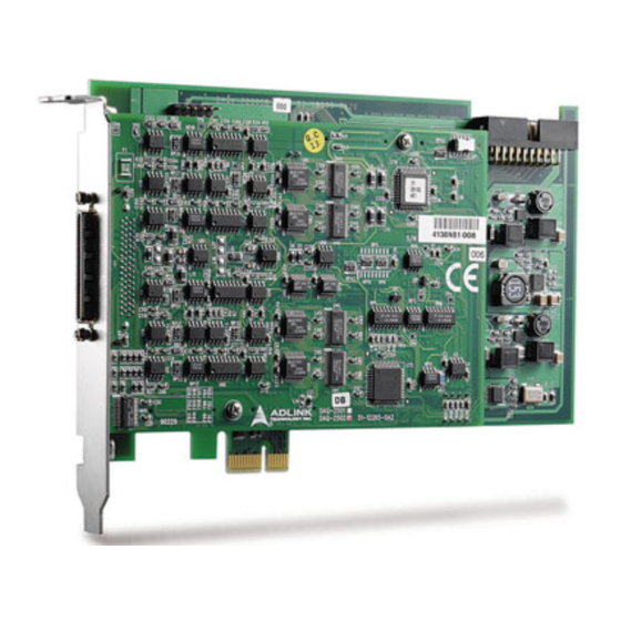
2.3 DAQ/PXI-2500 SERIES Layout Figure 2-1: PCB Layout of DAQ-2502/2501 Figure 2-2: PCB Layout of PXI-2502/2501 Installation... -
Page 20: Pci Configuration
2.4 PCI Configuration 1. Plug and Play: As a plug and play component, the board requests an interrupt number via its PCI controller. The system BIOS responds with an interrupt assignment based on the board information and system parameters. These system parameters are determined by the installed drivers and the hardware load seen by the sys- tem. -
Page 21: Signal Connections
Signal Connections This chapter describes the connectors of DAQ/PXI-2500 SERIES, and the signal connection between DAQ/PXI-2500 SERIES and external devices. 3.1 Connectors Pin Assignment DAQ/PXI-2500 SERIES is equipped with two 68-pin VHDCI-type con-nectors (AMP-787254-1). It is used for digital input / output, analog input / output, and timer/counter signals, etc. -
Page 22: Table 3-1: Connector Cn1 Pin Assignment
24 58 25 59 26 60 27 61 DGND 28 62 DGND 29 63 30 64 31 65 32 66 33 67 34 68 Table 3-1: Connector CN1 pin assignment Legend : Pin # Signal Name Reference Direction Description AO_<0..3> AGND Output Voltage output of DA channel <0..3>... - Page 23 Pin # Signal Name Reference Direction Description 31,65,32,66, PA<7,0> DGND Programmable DIO of 8255 Port A 33,67,34,68 35~46 AGND -------- -------- Analog ground External waveform trigger for AO 47,48 EXTWFTRIG_<A,B> DGND Input channel <0..3> <4..7> DGND Power(Output) +5V Power Source 28,50,54,62 DGND --------...
- Page 24 Signal Connections...
-
Page 25: Operation Theory
Operation Theory The operation theories of the DAQ/PXI-2500 series are described in this chapter. The functions include A/D conversion, D/A conver- sion, Digital I/O, and General Purpose Counter / Timer. This oper- ation theory will help you understand how to configure and program the DAQ/PXI-2500 series. -
Page 26: A/D Conversion
4.1 A/D Conversion When using an A/D converter, users should know the properties of the signal to be measured. In addition, users should setup the A/D configura-tions, including scan channels, input range, and polari- ties. The A/D acquisition is initiated by a trigger signal. The data acqui- sition will start once the trigger signal matches the trigger condi- tions. -
Page 27: Software Polling
Magnitude Unipolar Input Range Digital code Midscale - LSB 4.999389V 2.499694V 1.249847V 1.249923V 3FFF -FSR 2000 Table 4-2: Unipolar Input Range and Converted Digital Codes Software Polling This is the easiest way to acquire a single A/D data. The A/D con- verter performs one conversion whenever the dedicated software command is executed. -
Page 28: Table 4-3: Trigger Modes And Corresponding Trigger Sources
Please refer to Table 4-3 for a brief summary on Trigger Modes and their Trigger Sources. Trigger Trigger Mode Description Sources Post-Trigger Perform a scan right after the trigger occurs. Scan delayed by the amount of time pro- Software Trigger Delay-Trigger grammed after the trigger Digital Trigger... -
Page 29: Figure 4-1: Timing For Scan
The relationship between counters and acquisition timing is illus- trated in Figure 4-1. Figure 4-1: Timing for Scan NOTE: 1. The maximum A/D sampling rate is 400KHz for DAQ/ PXI-2500 series therefore the minimum setting of SI2_counter is 100. 2. The Scan Interval can not be smaller than the interval of data Sampling Interval multiple by the Number of chan- nels per Scan, i.e.: SI_counter >= SI2_counter * NumChan_Counter... - Page 30 formed after the trigger signal is specified by the PSC_counter, as illustrated in Figure 4.1.2. The total acquired data length = (number_of_channels_enabled_for _scan_acquisition) PSC_counter. Delay Trigger Acquisition Use delay trigger when users want to delay the scan after a trigger signal. The delay time is determined by the Delay_counter, as shown in Figure 4-3.
-
Page 31: Figure 4-2: Post Trigger
Figure 4-2: Post trigger Figure 4-3: Delay trigger Operation Theory... -
Page 32: Figure 4-4: Post Trigger With Retrigger
Figure 4-4: Post trigger with retrigger Bus-mastering DMA Data Transfer Bus Mastering DMA Mode In order to utilize the maximum PCI bandwidth, PCI bus-mas- tering DMA is used for high speed DAQ boards. The bus-mas- tering capability of the PLX PCI controller, takes over the PCI bus when it becomes the master. -
Page 33: Figure 4-5: Scatter/Gather Dma For Data Transfer
DMA with Scatter Gathering Capability In multi-user or multi-tasking OS such as Microsoft Windows, Linux, etc., it would be difficult to allocate a large continuous memory block due to memory fragmentation. PLX PCI control- ler provides scatter /gather or chaining mode to link non-contin- uous memory blocks into a linked list, so that users can transfer large amounts of data without being limited by the frag- ment of memory blocks. -
Page 34: D/A Conversion
4.2 D/A Conversion DAQ/PXI-2500 series offers flexible and versatile analog output scheme to fit users’ complex field applications. In order to take full advantages of DAQ/PXI-2500 series, we suggest users carefully read the following con-tents. Architecture There are up to 8-channel of 12-bit Digital-to-Analog Converter (DAC) available in the DAQ/PXI-2502. -
Page 35: Figure 4-7: Data Format In Fifo And Mapping
latched. This ensures D/A conversions to be synchronized for each channel in the same D/A group. Users can utilize this property to perform multi-channel waveform generation without any phase-lag. Hardware controlled Waveform Generation FIFO is a hardware first-in first-out data queue, which holds temporary digital codes for D/A conversion. -
Page 36: Table 4-5: D/A Output Versus Digital Codes
under heavy loading. Detailed function setup will be explained in Section 4.2.2. Note: When using waveform generation mode, all the four DACs in the same D/A group must be configured for the same mode. However, any one of the DAC can be disabled. If users need to use the software update mode, they can use another D/A group on the PXI/DAQ-2502. -
Page 37: Software Update
-FSR + LSB -Vref * (2046 / 2048) Vref * ( 1 / 4096) 0001 -FSR -Vref 0000 Table 4-5: D/A Output Versus Digital Codes DAQ/PXI-2500 SERIES can generate standard and arbitrary functions, continuously or piece-wisely. Appendix A demon- strates possible wave-form patterns generated by DAQ/PXI- 2500 SERIES in combination with various counters, clock sources, and voltage references. -
Page 38: Table 4-7: Summary Of Counters For Waveform Generation
Signal Descriptions Valid Sources Internal Update DAWR Write data to the DAC on the fal-ling edges of DAWR. External Update SSI Update Software Trigger Stop Stop Waveform Generation Ext. Digital Trigger Analog Trigger Table 4-6: Trigger Signals and Corresponding Signal Sources Waveform Generation Timing Six counters interact with the waveform to generate different DAWR timing, thus forming different waveforms. -
Page 39: Figure 4-8: Typical D/A Timing Of Waveform Generation
imum setting of UI_counter is 40. Figure 4-8: Typical D/A timing of waveform generation (Assuming the data in the data buffer are 2V, 4V, -4V, 0V) Trigger Modes Post-Trigger Generation Use post-trigger generation when users want to generate waveform right after a trigger signal. The number of patterns to be updated after the trigger signal is specified by UC_counter* IC_counter, as illustrated in Figure 4-9 Delay-Trigger Generation... - Page 40 The counter counts down on the rising edges of DLY1_counter clock source after the start trigger signal. When the count reaches zero, DAQ/PXI-2500 series starts to generate the waveform. The DLY1_counter clock source can be software selected from the Internal 40MHz Timebase, external clock input (AFI-0), or GPTC output 0/1.
-
Page 41: Figure 4-9: Post-Trigger Generation
Figure 4-9: Post-Trigger Generation Figure 4-10: Delay-Trigger Generation Operation Theory... -
Page 42: Figure 4-11: Post-Trigger With Retrigger Generation
Figure 4-11: Post-Trigger with Retrigger Generation Iterative Waveform Generation Users can set IC_counter to generate iterative waveforms, no matter which Trigger Mode is used. The IC_counter stores the iteration number. Examples are shown in Figure 4-12 and 4-13. When IC_counter is disabled, the waveform generation will not stop until a stop trigger is asserted. -
Page 43: Figure 4-12: Finite Iterative Waveform Generation W/Post-Trigger
will be a 1/8-cycle sine wave for every waveform period. In other words, a complete sine wave will be generated for every 8-iterations. If value specified in UC_counter is larger than the sample size of waveform LUT, say, 32; the generated wave- form will be a 2-cycle sine wave for every waveform period. -
Page 44: Figure 4-13: Infinite Iterative Waveform Generation W/Post-Trigger
Figure 4-13: Infinite iterative waveform generation w/Post-trigger (Assuming the digital codes in the FIFO are 2V, 4V, 2V, 0V) DLY2_Counter in iterative Waveform Generation To expand the flexibility of Iterative Waveform Generation, DLY2_counter was implemented to separate consecutive waveform generations. The DLY2_counter starts counting down right after a single waveform generation is completed. - Page 45 After a mode I stop trigger is asserted, the waveform genera- tion stops immediately. Figure 4-14 illustrates an example. Stop Mode II After a mode II stop trigger is asserted, the waveform genera- tion continues to generate a complete waveform then stops the operation.
-
Page 46: Figure 4-14: Stop Mode I
Figure 4-14: Stop mode I (Assuming the data in the data buffer are 2V, 4V, 2V, 0V) Figure 4-15: Stop mode II Operation Theory... -
Page 47: General Purpose Digital I/O
Figure 4-16: Stop mode III 4.3 General Purpose Digital I/O DAQ/PXI-2500 SERIES provides 24-line general-purpose digital I/ O (GPIO) through a 82C55A chip. The 24-line GPIO are separated into three ports: Port A, Port B and Port C. High nibble (bit[7…4]), and low nibble (bit[3…0]) of each port can be indi-vidually programmed to be either inputs or outputs. -
Page 48: General Purpose Timer/Counter Operation
4.4 General Purpose Timer/Counter Operation Two independent 16-bit up/down timer/counter are embedded in FPGA firmware for users applications. They have the following features: Direction of counting can be controlled via hardware or soft- ware. Selectable counter clock source from either internal or external clock up to 10MHz. -
Page 49: General Purpose Timer/Counter Modes
General Purpose Timer/Counter modes Eight programmable timer/counter modes are provided. modes start operations following the software start command. The GPTC software reset command initializes the status of the counter and re-loads the initial value to the counter. Mode1: Simple Gated-Event Counting In this mode, the counter counts the number of pulses on the GPTC_CLK after the software start. -
Page 50: Figure 4-18: Mode 2 Operation
count value can be read-back by software. Figure 4-18 illus- trates the operation where initial count = 0, up-counting mode. Figure 4-18: Mode 2 Operation Mode3: Single Pulse-width Measurement In this mode, the counter counts the pulse-width of the signal on GPTC_GATE in terms of GPTC_CLK. -
Page 51: Figure 4-20: Mode 4 Operation
enable/disable counting. When GPTC_GATE is inactive, the counter halts the counting. Figure 4-20 il-lustrates the genera- tion of a single pulse with pulse-delay of two and pulse-width of four. Figure 4-20: Mode 4 Operation Mode5: Single Triggered Pulse Generation This function generates a single pulse with programmable delay and pro-grammable pulse-width following an active GPTC_GATE edge. -
Page 52: Figure 4-22: Mode 6 Operation
After the software start, every active GPTC_GATE edge trig- gers a single pulse with programmable delay and pulse-width. Any GPTC_GATE trigger that occurs during the pulse genera- tion would be ignored. Figure 4-22 illustrates the generation of two pulses with pulse delay of two and pulse-width of four. Figure 4-22: Mode 6 Operation Mode7: Single Triggered Continuous Pulse Generation This mode is similar to mode 5, except that the counter gener-... -
Page 53: Trigger Sources
value. Figure 4-24 illustrates the generation of two pulses with pulse delay of four and pulse-width of three. Figure 4-24: Mode 8 Operation 4.5 Trigger Sources We provide flexible trigger selections in DAQ/PXI-2500 SERIES. In addi-tion to software trigger, DAQ/PXI-2500 SERIES also sup- ports external analog and digital triggers. -
Page 54: Table 4-8: Analog Trigger Src1(Extatrig) Ideal Transfer Characteristic
Figure 4-25: Analog trigger block diagram Trigger Level digital setting Trigger voltage 0xFF 9.92V 0xFE 9.84V 0x81 0.08V 0x80 0x7F -0.08V 0x01 -9.92V 0x00 -10V Table 4-8: Analog trigger SRC1(EXTATRIG) ideal transfer characteristic The trigger signal asserts when an analog trigger condition is meet. -
Page 55: Figure 4-26: Below-Low Analog Trigger Condition
Figure 4-26: Below-Low analog trigger condition Above-High analog trigger condition Figure 4-27 shows the above-high analog trigger condition, the trigger signal asserts when the input analog signal is higher than the High_Threshold voltage. The Low_Threshold setting is not used in this trigger condition. Figure 4-27: Above-High analog trigger condition Inside-Region analog trigger condition Figure 4-28 shows the inside-region analog trigger condition,... -
Page 56: Figure 4-28: Inside-Region Analog Trigger Condition
Figure 4-28: Inside-Region analog trigger condition High-Hysteresis analog trigger condition Figure 4-29 shows the high-hysteresis analog trigger condition, the trigger signal asserts when the input analog signal level is higher than the High_Threshold voltage, where the hysteresis region is determined by the Low_Threshold voltage. Figure 4-29: High-Hysteresis analog trigger condition Low-Hysteresis analog trigger condition Figure 4-30 shows the low-hysteresis analog trigger condition,... -
Page 57: Timing Signals
Figure 4-30: Low-Hysteresis analog trigger condition 4.6 Timing Signals In order to meet the requirements for user-specific timing or syn- chronizing multiple boards, DAQ/PXI-2500 SERIES provides a flexible interface for connecting timing signals with external cir- cuitry or other boards. The DAQ timing of the DAQ/PXI-2500 SERIES is composed of a bunch of counters and trigger signals in the FPGA on board. -
Page 58: System Synchronization Interface
Figure 4-31: DAQ signals routing System Synchronization Interface SSI uses bi-directional I/O to provide flexible connections between boards. You can choose each of the 7 timing signals and which board to be the SSI master. The SSI master can drive the timing signals of the slaves. -
Page 59: Calibration
Calibration This chapter introduces the calibration process to minimize AD meas-urement errors and DA output errors. DAQ/PXI-2500 SERIES is factory calibrated before shipment. The on-board high precision band-gap voltage reference together with TrimDAC compensates for unwanted offsets and gain errors, caused by environment variation or component aging. -
Page 60: Saving Calibration Constants
5.2 Saving Calibration Constants An on-board EEPROM is used to store calibration constants. In addition to a default bank that stores factory calibration constants, there are three user banks. Users can save the subsequently per- formed calibration constants in anyone of these user banks. ADLink provides software for users to save calibration constants in an easy manner. -
Page 61: Appendix
Appendix Waveform Generation Demonstration Combined with 6 counters, selectable trigger sources, external ref- erence sources, and time base, DAQ/PXI-2500 SERIES provides the capabilities to generate complex waveforms. Various modes shown below can be mixed together to generate waveforms that are even more complex. Although users can always load a new waveform to generate any desired waveform, we suggest using hardware capabilities to maximize both efficiency and flexibility. - Page 62 Iterative Generation w. Intermediate Space Utilize DLY2_counter to separate con-secutive waveform generations in itera-tive generation mode. In this demo, the original standard sine wave is repeated several times as specified in IC_counter, with intermedi-ate space determined by DLY2_counter. Piece-wise Generation When the value specified in UC_counter is smaller than the sample size of waveform, the waveform is generated piece-wisely.
-
Page 63: Warranty Policy
Warranty Policy Thank you for choosing ADLINK. To understand your rights and enjoy all the after-sales services we offer, please read the follow- ing carefully. 1. Before using ADLINK’s products please read the user man- ual and follow the instructions exactly. When sending in damaged products for repair, please attach an RMA appli- cation form which can be downloaded from: http:// rma.adlinktech.com/policy/. - Page 64 3. Our repair service is not covered by ADLINK's guarantee in the following situations: Damage caused by not following instructions in the User's Manual. Damage caused by carelessness on the user's part dur- ing product transportation. Damage caused by fire, earthquakes, floods, lightening, pollution, other acts of God, and/or incorrect usage of voltage transformers.
Need help?
Do you have a question about the NuDAQ-2500 Series and is the answer not in the manual?
Questions and answers