Sign In
Upload
Manuals
Brands
ADLINK Technology Manuals
PCI Card
NuDAQ-2500 Series
ADLINK Technology NuDAQ-2500 Series Manuals
Manuals and User Guides for ADLINK Technology NuDAQ-2500 Series. We have
2
ADLINK Technology NuDAQ-2500 Series manuals available for free PDF download: User Manual
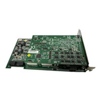
ADLINK Technology NuDAQ-2500 Series User Manual (66 pages)
High Performance Analog Output Multi-function Cards
Brand:
ADLINK Technology
| Category:
I/O Systems
| Size: 3 MB
Table of Contents
Table of Contents
6
List of Tables
8
Introduction
10
Features
10
Applications
11
Specifications
12
Analog Output (AO)
12
Analog Input (AI)
13
General Purpose Digital I/O (G
13
General Purpose Timer/ Counter (GPTC)
14
Analog Trigger (A.trig)
14
System Synchronous Interface (SSI)
14
Calibration
14
Physical
14
Operating Environment
15
Storage Environment
15
Software Support
15
Programming Library
15
D2K-LVIEW: Labview® Driver
16
D2K-OCX: Activex Controls
16
Installation
18
Contents of Package
18
Unpacking
18
DAQ/PXI-2500 SERIES Layout
20
Figure 2-1: PCB Layout of DAQ-2502/2501
20
Figure 2-2: PCB Layout of PXI-2502/2501
20
PCI Configuration
21
Signal Connections
22
Connectors Pin Assignment
22
Table 3-1: Connector CN1 Pin Assignment
23
Table 3-2: Connector CN2 Pin Assignment
23
Operation Theory
26
A/D Conversion
27
DAQ/PXI-2500 Series AD Data Format
27
Table 4-1: Bipolar Input Range and Converted Digital Codes
27
Table 4-2: Unipolar Input Range and Converted Digital Codes
27
Software Polling
28
Programmable Scan
28
Table 4-3: Trigger Modes and Corresponding Trigger Sources
29
Table 4-4: Summary of Counters for Programmable Scan
29
Figure 4-1: Timing for Scan
30
Figure 4-2: Post Trigger
32
Figure 4-3: Delay Trigger
32
Figure 4-4: Post Trigger with Retrigger
33
Figure 4-5: Scatter/Gather DMA for Data Transfer
34
D/A Conversion
35
Figure 4-6: Block Diagram of D/A Group
35
Figure 4-7: Data Format in FIFO and Mapping
36
Table 4-5: D/A Output Versus Digital Codes
37
Software Update
38
Waveform Generation
38
Table 4-6: Trigger Signals and Corresponding Signal Sources
38
Table 4-7: Summary of Counters for Waveform Generation
39
Figure 4-8: Typical D/A Timing of Waveform Generation
40
Figure 4-9: Post-Trigger Generation
42
Figure 4-10: Delay-Trigger Generation
42
Figure 4-11: Post-Trigger with Retrigger Generation
43
Figure 4-12: Finite Iterative Waveform Generation W/Post-Trigger
44
Figure 4-13: Infinite Iterative Waveform Generation W/Post-Trigger
45
Figure 4-14: Stop Mode I
47
Figure 4-15: Stop Mode II
47
General Purpose Digital I/O
48
Figure 4-16: Stop Mode III
48
General Purpose Timer/Counter Operation
49
Timer/Counter Functions Basics
49
General Purpose Timer/Counter Modes
50
Figure 4-17: Mode 1 Operation
50
Figure 4-18: Mode 2 Operation
51
Figure 4-19: Mode 3 Operation
51
Figure 4-20: Mode 4 Operation
52
Figure 4-21: Mode 5 Operation
52
Figure 4-22: Mode 6 Operation
53
Figure 4-23: Mode 7 Operation
53
Trigger Sources
54
Software-Trigger
54
External Analog Trigger
54
Figure 4-24: Mode 8 Operation
54
Table 4-8: Analog Trigger SRC1(EXTATRIG) Ideal Transfer Characteristic
55
Figure 4-25: Analog Trigger Block Diagram
55
Figure 4-26: Below-Low Analog Trigger Condition
56
Figure 4-27: Above-High Analog Trigger Condition
56
Figure 4-28: Inside-Region Analog Trigger Condition
57
Figure 4-29: High-Hysteresis Analog Trigger Condition
57
Timing Signals
58
Figure 4-30: Low-Hysteresis Analog Trigger Condition
58
System Synchronization Interface
59
Figure 4-31: DAQ Signals Routing
59
Calibration
60
Auto-Calibration
60
Saving Calibration Constants
61
Loading Calibration Constants
61
Appendix
62
Waveform Generation Demonstration
62
Warranty Policy
64
Advertisement
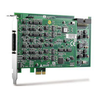
ADLINK Technology NuDAQ-2500 Series User Manual (64 pages)
High Performance Analog Output Multi-function Cards
Brand:
ADLINK Technology
| Category:
PCI Card
| Size: 0 MB
Table of Contents
Table of Contents
5
List of Tables
7
1 Introduction
9
Features
9
Applications
10
Specifications
11
Analog Output (AO)
11
Analog Input (AI)
12
General Purpose Digital I/O (G
12
General Purpose Timer/ Counter (GPTC)
13
Analog Trigger (A.trig)
13
System Synchronous Interface (SSI)
13
Calibration
13
Physical
13
Operating Environment
14
Storage Environment
14
Software Support
14
Programming Library
14
D2K-LVIEW: Labview® Driver
15
D2K-OCX: Activex Controls
15
2 Installation
17
Contents of Package
17
Unpacking
17
DAQ/PXI-2500 SERIES Layout
19
Figure 2-1: PCB Layout of DAQ-2502/2501
19
Figure 2-2: PCB Layout of PXI-2502/2501
19
PCI Configuration
20
3 Signal Connections
21
Connectors Pin Assignment
21
Table 3-1: Connector CN1 Pin Assignment
22
Table 3-2: Connector CN2 Pin Assignment
22
4 Operation Theory
25
A/D Conversion
26
DAQ/PXI-2500 Series AD Data Format
26
Table 4-1: Bipolar Input Range and Converted Digital Codes
26
Table 4-2: Unipolar Input Range and Converted Digital Codes
26
Software Polling
27
Programmable Scan
27
Table 4-3: Trigger Modes and Corresponding Trigger Sources
28
Table 4-4: Summary of Counters for Programmable Scan
28
Figure 4-1: Timing for Scan
29
Figure 4-2: Post Trigger
31
Figure 4-3: Delay Trigger
31
Figure 4-4: Post Trigger with Retrigger
32
Figure 4-5: Scatter/Gather DMA for Data Transfer
33
D/A Conversion
34
Figure 4-6: Block Diagram of D/A Group
34
Figure 4-7: Data Format in FIFO and Mapping
35
Table 4-5: D/A Output Versus Digital Codes
36
Software Update
37
Table 4-6: Trigger Signals and Corresponding Signal Sources
37
Waveform Generation
37
Table 4-7: Summary of Counters for Waveform Generation
38
Figure 4-8: Typical D/A Timing of Waveform Generation
39
Figure 4-10: Delay-Trigger Generation
41
Figure 4-9: Post-Trigger Generation
41
Figure 4-11: Post-Trigger with Retrigger Generation
42
Figure 4-12: Finite Iterative Waveform Generation W/Post-Trigger
43
Figure 4-13: Infinite Iterative Waveform Generation W/Post-Trigger
44
Figure 4-14: Stop Mode I
46
Figure 4-15: Stop Mode II
46
General Purpose Digital I/O
47
Figure 4-16: Stop Mode III
47
General Purpose Timer/Counter Operation
48
Timer/Counter Functions Basics
48
General Purpose Timer/Counter Modes
49
Figure 4-17: Mode 1 Operation
49
Figure 4-18: Mode 2 Operation
50
Figure 4-19: Mode 3 Operation
50
Figure 4-20: Mode 4 Operation
51
Figure 4-21: Mode 5 Operation
51
Figure 4-22: Mode 6 Operation
52
Figure 4-23: Mode 7 Operation
52
Trigger Sources
53
Software-Trigger
53
External Analog Trigger
53
Figure 4-24: Mode 8 Operation
53
Table 4-8: Analog Trigger SRC1(EXTATRIG) Ideal Transfer Characteristic
54
Figure 4-25: Analog Trigger Block Diagram
54
Figure 4-26: Below-Low Analog Trigger Condition
55
Figure 4-27: Above-High Analog Trigger Condition
55
Figure 4-28: Inside-Region Analog Trigger Condition
56
Figure 4-29: High-Hysteresis Analog Trigger Condition
56
Timing Signals
57
Figure 4-30: Low-Hysteresis Analog Trigger Condition
57
Figure 4-31: DAQ Signals Routing
58
System Synchronization Interface
58
5 Calibration
59
Auto-Calibration
59
Saving Calibration Constants
60
Loading Calibration Constants
60
Appendix
61
Waveform Generation Demonstration
61
Warranty Policy
63
Advertisement
Related Products
ADLINK Technology NuDAQ
ADLINK Technology NuDAQ 9112 Series
ADLINK Technology NuIPC
ADLINK Technology NuIPC 9112 Series
ADLINK Technology NuPRO-900A
ADLINK Technology NuDAQ ACL-6128
ADLINK Technology NuDAQ 723 Series
ADLINK Technology NuDAQ 6208 Series
ADLINK Technology NuDAQ PCI-6208-GL
ADLINK Technology NuDAQ PCI-6216-GL
ADLINK Technology Categories
Computer Hardware
Motherboard
PCI Card
Control Unit
Desktop
More ADLINK Technology Manuals
Login
Sign In
OR
Sign in with Facebook
Sign in with Google
Upload manual
Upload from disk
Upload from URL