
Related Manuals for ADLINK Technology NuDAQ 9112 Series


Summary of Contents for ADLINK Technology NuDAQ 9112 Series
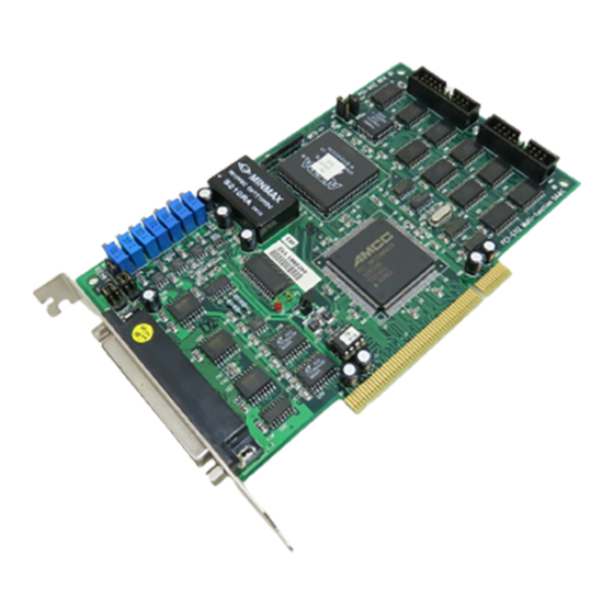
- Page 1 ® ® NuDAQ / NuIPC 9112 Series Multi-function DAS Cards for PCI / 3U CompactPCI User’s Manual...
- Page 2 Trademarks ® ® NuDAQ , NuIPC are registered trademarks of ADLINK Technology Inc. Other products names mentioned herein are used for identification purposes only and may be trademarks and/or registered trademarks of their respective companies.
- Page 3 Getting service from ADLINK Customer Satisfaction is always the most important thing for ADLINK Tech Inc. If you need any help or service, please contact us and get it. ADLINK Technology Inc. Web Site http://www.adlink.com.tw Sales & Service service@adlink.com.tw Technical NuDAQ nudaq@ADLINK.com.tw...
-
Page 5: Table Of Contents
CONTENTS Chapter 1 Introduction ........... 1 Features................1 Applications................. 2 Specifications ..............2 Software Supporting............4 1.4.1 Programming Library ................4 ® 1.4.2 PCIS-LVIEW: LabVIEW Driver............4 1.4.3 PCIS-VEE: HP-VEE Driver..............5 1.4.4 DAQBench : ActiveX Controls ............5 1.4.5 DASYLab PRO .................. - Page 6 A/D control Register ............22 A/D Status Register ............25 Software Trigger Register...........25 Digital I/O register...............26 Internal Timer/Counter Register..........27 High Level Programming............27 3.10 Low Level Programming.............27 Chapter 4 Operation Theorem......28 A/D Conversion..............28 Analog Input Signal Connection .........28 4.2.1 A/D Conversion Procedure...............31 4.2.2 A/D Trigger Modes ................31 4.2.3 A/D Data Transfer Modes..............32...
- Page 7 5.21 _9112_ContDmaStop ............58 5.22 _9112_AD_INT_Start ............59 5.23 _9112_AD_INT_Status ............60 5.24 _9112_AD_INT_Stop ............61 5.25 _9112_AD_Timer..............61 5.26 _9112_TIMER_Start.............63 5.27 _9112_TIMER_Read ............63 5.28 _9112_TIMER_Stop .............64 5.29 _9112_Alloc_DMA_Mem .............64 5.30 _9112_Free_DMA_Mem............65 5.32 _9112_Get_Sample .............65 Chapter 6 Calibration..........67 What do you need...............67 VR Assignment ..............68 A/D Adjustment..............68 6.3.1 Bipolar Calibration ................68...
- Page 8 How to Use This Guide This manual is for helping users to manipulate the PCI-9112 and cPCI- 9112. The functionality of PCI-9112 and cPCI-9112 are the same. Therefore, the “PCI-9112” in this manual represent both the PCI-9112 and cPCI-9112 without specifications. The manual describes how to modify various settings on the PCI-9112 card to meet your requirements.
-
Page 9: Chapter 1 Introduction
I n t r o d u c t i o n The 9112 series products are multi-function data acquisition cards.. The 9112 series includes: PCI-9112: 12-bit 100KHz Multifunction DAS card cPCI-9112: 12-bit 100KHz Multifunction DAS card for 3U ComptactPCI The 9112 series DAS cards are using state-of-the-art technology to make this card ideal for data logging and signal analysis applications in medical, process control, etc. -
Page 10: Applications
Ø 37-pin D-type connector for PCI-9112 Ø 100-pin SCSI-type connector for cPCI-9112 Ø Half-size PCB Applications Ø Industrial and laboratory ON/OFF control Ø Energy management Ø Annunciation Ø 16 TTL/DTL compatible digital input channels Ø Security controller Ø Product test Ø... - Page 11 Ø External Reference: (unipolar) max. +10V or -10V Ø Converter: DAC7541 or equivalent, monolithic multiplying Settling Time: 30 µ sec Ø Linearity: ±1/2 bit LSB Ø Output Driving Capability: ±5mA max. Ø Digital I/O (DIO) Ø Numbers of channels: 16 TTL compatible inputs and outputs Ø...
-
Page 12: Software Supporting
Software Supporting ADLink provides versatile software drivers and packages for users’ different approach to built-up a system. We not only provide programming library such as DLL for many Windows systems, but also ® provide drivers for many software package such as LabVIEW , HP , DASYLab , InTouch... -
Page 13: Pcis-Vee: Hp-Vee Driver
1.4.3 PCIS-VEE: HP-VEE Driver The PCIS-VEE includes the user objects, which are used to interface with HP VEE software package. PCIS-VEE supports Windows 95/98/NT. The HP-VEE drivers are free shipped with the board. You can install and use them without license. For detail information about PCIS-VEE, please refer to the user’s guide in the CD. -
Page 14: Chapter 2 Installation
I n s t a l l a t i o n This chapter describes how to install the 9112 series cards. Please follow the follow steps to install. Check what you have (section 2.1) Unpacking (section 2.2) Check the PCB and jumper location(section 2.3) Setup jumpers (section 2.4~2.8) Install the hardware and setup and jumpers (section 2.10) Install the software drivers and run utility to test (section 2.11) -
Page 15: Unpacking
Unpacking The card contains sensitive electronic components that can be easily damaged by static electricity. Failure to perform the procedure outlined below may damage the on board devices. The board is packaged in an anti-static bag to avoid damage to the sensitive IC on the board. -
Page 16: Pcb Layout
PCB Layout PCI-9112 Layout Figure 2.1 PCB Layout of the PCI-9112 8 • Installation... - Page 17 cPCI-9112 Layout Figure 2.2 PCB Layout of the PCI-9112 Installation • 9...
-
Page 18: Jumper Settings
Jumper Settings You can set the following configuration by jumpers: the analog input signal mode, counter’s clock source, and analog output range. The card's jumpers and switches are preset at the factory. You can change the jumper settings for your own applications. For system reliability and safety, the design of PCI-9112 still keeps some board configurations to be set through jumpers. -
Page 19: Clock Source Setting
PCI-9112 cPCI-9112 SINGLE SINGLE SINGLE SINGLE Single-ended (default setting) DIFF DIFF DIFF DIFF SINGLE SINGLE SINGLE SINGLE Differential Input DIFF DIFF DIFF DIFF Figure 2.2 Analog Input Mode Setting Clock Source Setting The programmable interval timer 8254 is used in the PCI-9112. It provides 3 independent 16-bit programmable down counters. - Page 20 JP4(PCI-9112) JP5(cPCI-9112) D/A CH1 is External INTREF INTREF D/A CH2 is External ExtRef1 ExtRef2 INTREF INTREF D/A CH1 is External D/A CH2 is Internal ExtRef1 ExtRef2 D/A CH1 is Internal INTREF INTREF D/A CH2 is External ExtRef1 ExtRef2 D/A CH1 is Internal INTREF INTREF D/A CH2 is Internal...
-
Page 21: Connectors Pin Assignments
Connectors Pin Assignments 2.9.1 Pin Assignments of PCI-9112 The PCI-9112 comes equipped with two 20-pin insulation displacement connectors - CN1 and CN2 and one 37-pin D-type connector - CN3. The CN1 and CN2 are located on board and CN3 located at the rear plate. CN1 is for digital signal input, CN2 for digital signal output, CN3 for analog input, analog output and timer/counter's signals. - Page 22 GATE : Gate input for 8254 COUT n : Signal output of Counter n V.ERF : Voltage Reference A.GND : Analog Ground : Ground CN 1: Digital Signal Input (DI 0 - 15) DI 1 DI 0 DI 3 DI 2 DI 5 DI 4 DI 7...
-
Page 23: Pin Assignments Of Cpci-9112
2.9.2 Pin Assignments of cPCI-9112 (1) DOUT_0 (26) DIN_9 (51) (51) (76) GND (52) (2) DOUT_1 (27) DIN_10 (52) (53) (77) GND (3) DOUT_2 (28) DIN_11 (53) (78) GND (4) DOUT_3 (29) DIN_12 (54) (79) GND (5) DOUT_4 (30) DIN_13 (55) (80) GND (6) DOUT_5 (31) DIN_14... -
Page 24: Hardware Installation Outline
2.10 Hardware Installation Outline PCI configuration The PCI cards (or CompactPCI cards) are equipped with plug and play PCI controller, it can request base addresses and interrupt according to PCI standard. The system BIOS will install the system resource based on the PCI cards’... -
Page 25: Daughter Board Connection
2.12 Daughter Board Connection The PCI-9112 can be connected with five different daughter boards, ACLD-8125, 9137, 9138, 9182, 9185, and 9188. The functionality and connections are specified in the following sections. The cPCI-9112 is equipped with 100 pin SCSI-II type connector, the DIN- 100S is a general purpose terminal board for connecting the external devices. -
Page 26: Connect With Acld-9185
2.12.4 Connect with ACLD-9185 The ACLD-9185 is a 16 channel SPDT relay output board. This board is connected with CN2 of PCI-9112 via 20-pin flat cable. by using this board, you can control outside device through the digital output signals. 2.12.5 Connect with ACLD-9138 and ACLD-9188 ACLD-9138 and ACLD-9188 are general purpose terminal boards for all the card which comes equipped with 37-pin D-sub connector. -
Page 27: Chapter 3 Registers Format
R e g i s t e r s F o r m a t The detailed descriptions of the register format and structure of the PCI- 9112 are specified in this chapter. This information is quite useful for the programmer who wish to handle the card by low-level program. -
Page 28: A/D Data Registers
I/O Address Read Write Base + 0 Counter 0 Counter 0 Base + 4 Counter 1 Counter 1 Base + 8 Counter 2 Counter 2 Base + C ------------- 8254 Counter Control Base + 10 A/D Data Reg. Data Reg. Base + 14 ------------- Data... -
Page 29: D/A Output Register
D/A Output Register The D/A converter will convert the D/A output register data to the analog signal. The register data of the address Base+10 is used for D/A channel 1, Base+14 is used for D/A channel 2. Address : BASE + 10 Attribute : write only Data Format: (for D/A Channel 1) -
Page 30: A/D Control Register
A/D control Register This register is to control the A/D channels to be converted. It is a write only register. When the channel number is written to the register, the multiplexer switches to the new channel and wait for conversion. Address : BASE + 18 Attribute... - Page 31 Only below modes are legal to be applied on the PCI-9112 card : Bit 3 Mode Description Software Trigger & Polling Timer Pacer Trigger & Timer Pacer Trigger & INT External Trigger & Polling External Trigger & DMA External Trigger & INT Auto-Scan: ( Bit 4) 0: Auto Scan is disabled Only channel [M3 M2 M1 M0] is converted only...
- Page 32 In PCI-9112, the analog input ranges are software programmable and it is controlled by the gain value. The gain value and its corresponding input range is shown as below. Bipola Input Range Unipol ±10V Bipola ±5V Bipola ±2.5V Bipola ±1.25V Bipola ±0.625V Bipola...
-
Page 33: A/D Status Register
A/D Status Register Address : BASE + 18 Attribute : read only Data Format: Base + 18 Base + 19 Base + 1A Base + 1B DOVR: A/D Over-Run ( it is only when A/D is transferred by DMA bus master mode. -
Page 34: Digital I/O Register
Digital I/O register There are 16 digital input channels and 16 digital output channels provided by the PCI-9112. The address Base + 1C is used to access digital inputs and control digital outputs. Address : BASE + 1C Attribute : read only Data Format: Address : BASE + 1C... -
Page 35: Internal Timer/Counter Register
Internal Timer/Counter Register Two counters of 8254 are used for periodically triggering the A/D conversion, the left one is left free for user applications. The 8254 occupies 4 I/O address locations in the PCI-9112 as shown blow. Users can refer to NEC's or Intel's data sheet for a full description of the 8254 features. -
Page 36: Chapter 4 Operation Theorem
O p e r a t i o n T h e o r e m The operation theorem of the functions on PCI-9112 card is described in this chapter. The functions include the A/D conversion, D/A conversion, Digital I/O and counter / timer. The operation theorem can help you to understand how to manipulate or to program the PCI-9112. - Page 37 Single-ended Mode The single-ended mode has only one input relative to ground and it suitable for connecting with the floating signal source. The floating source means it does not have any connection to ground. Figure 3.4 shows the single-ended connection. Note that when more than two floating sources are connected, the sources must be with common ground.
- Page 38 A differential mode must be used when the signal source is differential. A differential source means the ends of the signal are not grounded. To avoid the danger of high voltage between the local ground of signal and the ground of the PC system, a shorted ground path must be connected. Figure 3.6 shows the connection of differential source.
-
Page 39: A/D Conversion Procedure
4.2.1 A/D Conversion Procedure The A/D conversion is starting by a trigger source, then the A/D converter will start to convert the signal to a digital value. The PCI-9112 provides three trigger modes, s ee section 5.1.2. While A/D conversion, the DRDY bit in A/D status register is cleared to indicate the data is not ready. -
Page 40: A/D Data Transfer Modes
External Trigger Through the pin-17 of CN3 ( ExtTrig), the A/D conversion also can be performed when a rising edge of external signal is occurred. The conversion rate of this mode is more flexible than the previous two modes, because the users can handle the external signal by outside device. The external trigger can combine with the DMA transfer, interrupt data transfer, or even program polling data transfer. -
Page 41: D/A Conversion
DMA Transfer (DMAX) The DMA (Direct Memory Access) bus master allows data to be transferred directly between the PCI-9112 and the PC memory at the fastest possible rate, without using any CPU time. The A/D data will be queue at local FIFO on the PCI-9112 itself and it is automatically transferred to PC's memory. -
Page 42: Digital Input And Output
Digital Input and Output The PCI-9112 provides 16 digital input and 16 digital output channels through the connector CN1 and CN2 on board. The digital I/O signal are fully TTL/DTL compatible. The detailed digital I/O signal are specified in section 1.3. To program digital I/O operation is fairly straight forward. -
Page 43: Timer/Counter Operation
Timer/Counter Operation The PCI-9112 has an interval timer/counter 8254 on board. It offers 3 independent 16-bit programmable down counters; counter 1 and counter 2 are cascaded together for A/D timer pacer trigger of A/D conversion, and counter 0 is free for your applications. Figure 3.10 shows the 8254 timer/counter connection. - Page 44 Ø event counter Ø binary rate multiplier Ø real-time clock Ø Digital one-shot Ø motor control For more information about the 8254, please refer to the NEC Microprocessors and peripherals or Intel Microsystems Components Handbook. Pacer Trigger Source The counter 1 and counter 2 are cascaded together to generate the timer pacer trigger of A/D conversion.
- Page 45 Control Byte Before loading or reading any of these individual counters, the control byte (BASE+3) must be loaded first. The format of the control byte is : • SC1 & SC0 - Select Counter (Bit7 & Bit 6) COUNTER Select Counter 0 Select Counter 1 Select Counter 2 ILLEGAL...
- Page 46 • BCD - Select Binary/BCD Counting (Bit 0) 16-BITS BINARY COUNTER BINARY CODED DECIMAL (BCD) COUNTER (4 DIGITAL) The count of the binary counter is from 0 up to 65,535 and the count of the BCD counter is from 0 up to 9,999 Mode Definitions In 8254, six operating modes can be selected.
-
Page 47: Chapter 5 C/C++ Library
C / C + + L i b r a r y This chapter describes the software library for operating this card. Only the functions in DOS library and Windows 95 DLL are described. Please refer to the PCIS-DASK function reference manual, which included in ADLINK CD, for the descriptions of the Windows 98/NT/2000 DLL functions. -
Page 48: Programming Guide
Programming Guide 5.2.1 Naming Convention The functions of the NuDAQ PCI cards or NuIPC CompactPCI cards’ software driver are using full-names to represent the functions' real meaning. The naming convention rules are: In DOS Environment : _{hardware_model}_{action_name}. e.g. _9112_Initial(). All functions in PCI-9112 driver are with 9112 as {hardware_model}. But they can be used by PCI-9112, cPCI-9112. -
Page 49: 9112_Initial
_9112_Initial @ Description A PCI-9112 card is initialized according to the card number. Becaus e the PCI-9112 is PCI bus architecture and meets the plug and play design, the IRQ and base_address (pass-through address) are assigned by system BIOS directly. Every PCI-9112 card has to be initialized by this function before calling other functions. - Page 50 exit(0); errCode = _9112_Initial( CARD_2, &baseAddr2, &irqNo2); if ( errCode != ERR_NoError ) exit(0); _9112_DI @ Description This function is used to read data from digital input port. There are 16-bit digital inputs on the PCI-9112. You can get all 16 input data from _9112_DI one shot.
- Page 51 Syntax Visual C++ (Windows-95) int W_9112_DI_Channel (int card_number, int di_ch_no, unsigned int *di_data) Visual Basic (Windows-95) W_9112_DI_Channel (ByVal card_number As Long, ByVal di_ch_no As Long, di_data As Long) As Integer C/C++ ( DOS) int _9112_DI_Channel (int card_number, int di_ch_no, unsigned int *di_data ) Argument card_number :...
- Page 52 Syntax Visual C++ (Windows-95) int W_9112_DO (int card_number, unsigned int do_data) Visual Basic (Windows-95) W_9112_DO (ByVal card_number As Long, ByVal do_data As Long) As Integer C/C++ ( DOS) int _9112_DO(int card_number, unsigned int do_data ) Argument card_number : the card number of PCI-9112 do_data : value will be written to digital output port Return Code...
-
Page 53: 9112_Ad_Set_Channel
Example #include “9112.h” main() baseAddr, irqNo; _9112_Initial( CARD_1, &baseAddr, &irqNo); /* Assume NoError when Initialize PCI-9112 */ /* if the hardware setting for DA output range is 0~5V */ _9112_DA(CARD_1, DA_CH_1 , 0x800 ); printf( "The output voltage of CH1 is 2.5V \n"... -
Page 54: 9112_Ad_Set_Range
Return Code : ERR_NoError, ERR_BoardNoInit ERR_InvalidADChannel _9112_AD_Set_Range Description This function is used to set the A/D analog input range by means of writing data to the A/D range control register. There are two factors will change the analog input range - Gain and Input type. The Gain can be choice from 0.5, 1, 2, 4, and 8 . -
Page 55: 9112_Ad_Set_Mode
Syntax Visual C++ (Windows-95) int W_9112_ AD_Set_Range (int card_number, int ad_range) Visual Basic (Windows-95) W_9112_AD_Set_Channel (ByVal card_number As Long, ByVal ad_range As Long) As Long C/C++ ( DOS) int _9112_AD_Set_Range (int card_number, int ad_range ) Argument card_number : the card number of PCI-9112 ad_range : the programmable range of A/D conversion, please refer the the above table for the possible range values. -
Page 56: 9112_Ad_Set_Autoscan
Syntax Visual C++ (Window s-95) int W_9112_AD_Set_Mode (int card_number, int ad_mode) Visual Basic (Windows-95) W_9112_AD_Set_Mode (ByVal card_number As Long, ByVal ad_mode As Long) As Long C/C++ ( DOS) int _9112_AD_Set_Mode (int card_number, int ad_mode ) Argument card_number : the card number of PCI-9112 ad_mode : AD trigger and data transfer mode ( please refer to above table.) -
Page 57: 9112_Ad_Soft_Trig
4, 3, 2, 1, 0, 4, 3, 2, 1, 0, 4, 3, 2, 1, 0, 4, 3, ..If the auto-scan is set as disable, the channel will be kept as single channel only, such as channel 4. Syntax Visual C++ (Windows-95) int W_9112_AD_Set_Autoscan (int card_number, int autoscan) Visual Basic (Windows-95) int W_9112_AD_Set_ Autoscan (ByVal card_number As Long, ByVal... -
Page 58: 9112_Ad_Aquire
5.13 _9112_AD_Aquire Description This function is used to poll the AD conversion data. It will trigger the AD conversion, and read the 12-bit A/D data until the data is ready ('data ready' bit becomes low). Syntax Visual C++ (Windows-95) int W_9112_AD_Aquire (int card_number, int *ad_data) Visual Basic (Windows-95) W_9112_ AD_Aquire (ByVal card_number As Long, ad_data As Long )As Integer... -
Page 59: 9112_Ad_Dma_Start
5.14 _9112_AD_DMA_Start Description The function will perform A/D conversion N times with DMA data transfer. It takes place in the background which will not stop until the N -th conversion completed your program execute _9112_AD_DMA_Stop() function to stop the process. After executing this function, it is necessary to check the status of the operation by using the function _9112_AD_DMA_Status(). - Page 60 3. After the A/D conversion is started, the A/D converted data is stored in the FIFO of PCI controller. Each bus mastering data transfer continually tests if any data in the FIFO and then blocks transfer, the system will continuously loop until the conditions are satisfied again but will not exit the block transfer cycle if the block count is not complete.
-
Page 61: 9112_Ad_Dma_Status
ad_ch_no : A/D channel number ad_range : A/D analog input range, the possible values are shown in section 4.3.8. count : the number of A/D conversion ad_buffer(DOS) : the start address of the memory buffer to store the AD data, the buffer size must large than the number of AD conversion. In DOS environment, please make sure this memory is double-word alignment. -
Page 62: 9112_Ad_Dma_Stop
C/C++ ( DOS) int _9112_AD_DMA_Status(int card_number, int *status , int *count ) Argument card_number : the card number of PCI-9112 status : status of the DMA data transfer 0: AD_DMA_STOP : DMA is completed 1: AD_DMA_RUN : DMA is not completed count : the number of A/D data which has been transferred. -
Page 63: 9112_Contdmastart
5.17 _9112_ContDmaStart Description The function will perform A/D conversion continuous with DMA data transfer. It will takes place in the background which will not be stop until your program execute _9112_ContDmaStop() function to stop the process. After executing this function, it is necessary to check the status of double buffer by using the function _9112_CheckHalfReady() and using _9112_DblBufferTransfer() to get the A/D converted data. -
Page 64: 9112_Checkhalfready
AD data, the buffer size must large than the number of AD conversion. In DOS environment, please make sure this memory is double-word alignment. Every 16-bit unsigned integer data in ad_buffer: D11 D10 D9 .......D1 D0 C3 C2 C1 C0 D11, D10, ..., D1, D0 : A/D converted data C3, C2, C1, C0 : converted channel no. -
Page 65: 9112_Dblbuffertransfer
Argument card_number : the card number of PCI-9112 halfReady : TRUE or FALSE. Return Code ERR_NoError, ERR_BoardNoInit Example See Demo Program 'AD_DEMO5.C' 5.19 _9112_DblBufferTransfer Description Using this function to move the converted A/D data to user buffer. Syntax Visual C++ (Windows-95) int W_9112_DblBufferTransfer (int card_number, unsigned long far * userBuffer) Visual Basic (Windows-95) -
Page 66: 9112_Contdmastop
Visual Basic (Windows-95) W_9112_GetOverrunStatus(ByVal card_number As Long, overrunCount As Long) As Long C/C++ ( DOS) int _9112_GetOverrunStatus (int card_number, int *overrunCount ) Argument card_number : the card number of PCI-9112 overrunCount: number of overrun counts. Return Code ERR_NoError, ERR_BoardNoInit Example See Demo Program 'AD_DEMO5.C' 5.21 _9112_ContDmaStop Description... -
Page 67: 9112_Ad_Int_Start
5.22 _9112_AD_INT_Start Description The function will perform A/D conversion N times with interrupt data transfer. It takes place in the background which will not stop until the N-th conversion been completed your program execute _9112_AD_INT_Stop() function to stop the process. After executing this function, it is necessary to check the status of the operation by using the function 9112_AD_INT_Status(). -
Page 68: 9112_Ad_Int_Status
D11 D10 D9 .......D1 D0 C3 C2 C1 C0 D11, D10, ..., D1, D0 : A/D converted data C3, C2, C1, C0 : converted channel no. c1 : the 16-bit timer frequency divider of timer channel #1 c2 : the 16-bit timer frequency divider of timer channel #2 Return Code ERR_NoError, ERR_BoardNoInit... -
Page 69: 9112_Ad_Int_Stop
5.24 _9112_AD_INT_Stop @ Description This function is used to stop the interrupt data transfer function. After executing this function, the internal AD trigger is disable and the AD timer is stopped. The function returns the number of the data which has been transferred, no matter whether if the AD interrupt data transfer is stopped by this function or by the _9112_AD_INT_Stop() itself. - Page 70 Syntax Visual C++ (Windows-95) int W_9112_AD_Timer (int card_number, unsigned int c1, unsigned int c2) Visual Basic (Windows-95) W_9112_Timer (ByVal card_number As Long, c1 As Long, c2 As Long) As Long C/C++ ( DOS) int _9112_AD_Timer(int card_number, unsigned int c1 , unsigned int c2 ) Argument card_number :...
-
Page 71: 9112_Timer_Start
5.26 _9112_TIMER_Start Description The Timer #0 on the PCI-9112 can be freely programmed by the users. This function is used to program the Timer #0. This timer can be used as frequency generator if internal clock is used. It also can be used as event counter if external clock is used. -
Page 72: 9112_Timer_Stop
Argument : card_number : the card number of PCI-9112 counter_value : the counter value of the Timer #0 @ Return Code : ERR_NoError, ERR_BoardNoInit 5.28 _9112_TIMER_Stop Description This function is used to stop the timer operation. The timer is set to the 'One-shot' mode with counter value ' 0 '. -
Page 73: 9112_Free_Dma_Mem
Argument : buf_size: Bytes to allocate. Please be careful, the unit of this argument is BYTE, not SAMPLE. memID: If the memory allocation is successful, driver returns the ID that memory this argument. this memory W_9112_AD_DMA_Start or W_9112_ContDmaStart function call. linearAddr: The linear address of the allocated DMA memory. - Page 74 Argument : linearAddr: The linear address of the allocated DMA memory. index: The index of the sample to retrieve. The first sample is with index 0. ai_data: Returns the sample retrieved. Return Code : ERR_NoError 66 • C/C++ Library...
-
Page 75: Chapter 6 Calibration
C a l i b r a t i o n In data acquisition process, how to calibrate your measurement devices to maintain its accuracy is very important. Users can calibrate the analog input and analog output channels under the users' operating environment for optimizing the accuracy. -
Page 76: Vr Assignment
VR Assignment There are five variable resistors (VR) on the PCI-9112 board to allow you making accurate adjustment on A/D and D/A channels. The function of each VR is specified as Table 6.1. A/D bipolar offset adjustment A/D full scale adjustment D/A channel 1 full scale adjustment D/A channel 2 full scale adjustment A/D unipolar offset adjustment... -
Page 77: D/A Adjustment
D/A Adjustment There are two steps to calibrate the analog output channels, D/A 1 and D/A 2. The first step is to adjust the reference voltage, and the second step is to adjust each channel of D/A. 6.4.1 Reference Voltage Calibration Set reference voltage as -5V (the D/A reference voltage is selected by JP3, see section 2.8). -
Page 78: Chapter 7 Software Utilities
S o f t w a r e U t i l i t i e s The PCI-9112 is a PCI-based high performance m ulti-function data acquisition card, which provides 16 single-ended analog or 8 differential analog inputs and auto scan channel by hardware, two double-buffered multiplexing analog outputs. -
Page 79: Running The Utility
7.1.1 Running the Utility After finishing the installation, you can execute the utility by typing as follows : C> cd \ADLINK\9112\DOS\UTIL C> 9112UTIL The 9112UTIL.EXE includes six functions: 1. Configuration : Check the hardware setting of your PCI-9112. 2. Calibration : Calibrate the A/D and D/A measurement accuracy of your PCI-9112. -
Page 80: Functional Testing
When you choose the calibration function from the main menu list, a diagram shown below is displayed on the screen, the upper window shows the calibration items, such as DAC channel 1 or channel 2 full range adjust, Gain Amplifier offset adjust. etc. The bottom window shows the detailed procedures should be followed when you proceed the calibration. -
Page 81: Appendix A. Demo. Programs
A p p e n d i x A . D e m o . P r o g r a m s DOS Software: In this software CD, there are 8 DOS demonstration programs are provided. They could help you to program your application by using C Language Library easily. - Page 82 The description of these programs are specified as follows: Samples \sdk\9112\ A/D conversion uses software trigger 9112util.exe and program data transfer. Visual C/C++ program. Samples \sdk\9112int\ A/D conversion uses interrupt data 9112int.exe transfer. Visual C/C++ program. Samples \sdk\9112dma\ A/D conversion uses DMA data 9112dma.exe transfer.
-
Page 83: Product Warranty/Service
P r o d u c t W a r r a n t y / S e r v i c e Seller warrants that equipment furnished will be free form defects in material and workmanship for a period of one year from the confirmed date of purchase of the original buyer and that upon written notice of any such defect, Seller will, at its option, repair or replace the defective item under the terms of this warranty, subject to the provisions and specific...
Need help?
Do you have a question about the NuDAQ 9112 Series and is the answer not in the manual?
Questions and answers