Advertisement
Quick Links
www.ti.com
EVM User's Guide: LMKDB1108EVM
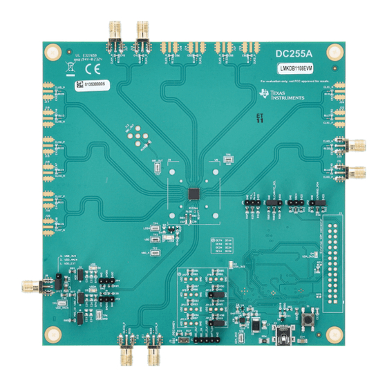
LMKDB1108 Evaluation Module
Description
The LMKDB1108 Evaluation Module (EVM) is
designed to provide a quick setup to evaluate the
LMKDB1108 LP-HCSL buffer that supports PCIe Gen
1 to Gen 6. The printed circuit board (PCB) contains
several jumpers and a USB connection to enable
the LMKDB1108 with desired user programming
and setup. The evaluation module provides flexibility
for compliance testing, system prototyping, and
performance evaluation of the LMKDB1108 device.
SNAU291A – OCTOBER 2023 – REVISED SEPTEMBER 2024
Submit Document Feedback
Features
•
PCIe Gen 1 to Gen 6
•
External and USB power supply options
•
Programmability through
graphical user interface (GUI)
•
Onboard input and output expander for output
enable and disable through pin controls
Applications
•
High performance computing
•
Server motherboard
•
NIC/SmartNIC
•
Hardware accelerator
LMKDB1108 EVM Default Settings
Copyright © 2024 Texas Instruments Incorporated
Description
TICS Pro Software GUI
LMKDB1108 Evaluation Module
1
Advertisement

Related Manuals for Texas Instruments LMKDB1108EVM


Summary of Contents for Texas Instruments LMKDB1108EVM
- Page 1 LMKDB1108 device. • High performance computing • Server motherboard • NIC/SmartNIC • Hardware accelerator LMKDB1108 EVM Default Settings SNAU291A – OCTOBER 2023 – REVISED SEPTEMBER 2024 LMKDB1108 Evaluation Module Submit Document Feedback Copyright © 2024 Texas Instruments Incorporated...
- Page 2 (LOS), and 3-wire or 4-wire SBI and SMBus interface. The EVM has integrated LDOs for excellent power supply noise suppression with operating supply voltage of 3.3V. LMKDB1108 Evaluation Module SNAU291A – OCTOBER 2023 – REVISED SEPTEMBER 2024 Submit Document Feedback Copyright © 2024 Texas Instruments Incorporated...
- Page 3 LMKDB1108 EVM Default Settings. Make sure to adjust the jumpers as shown for initial boot-up using USB power supply option. To begin using the LMKDB1108EVM, follow the steps below. 1. Verify the EVM default jumper as described in Table 2-1 LMKDB1108 EVM Default Settings.
- Page 4 TICS Pro instance, can blink at a slow rate of 1 second on, 1 second off continuously. d. Confirm all the fields match the ones shown in Figure 2-2. Figure 2-1. USB LED LMKDB1108 Evaluation Module SNAU291A – OCTOBER 2023 – REVISED SEPTEMBER 2024 Submit Document Feedback Copyright © 2024 Texas Instruments Incorporated...
- Page 5 2.3 EVM Measurements Measurements can now be made on the clock outputs using an oscilloscope or a phase noise analyzer. SNAU291A – OCTOBER 2023 – REVISED SEPTEMBER 2024 LMKDB1108 Evaluation Module Submit Document Feedback Copyright © 2024 Texas Instruments Incorporated...
- Page 6 14, 19, 30, and 34 since those pins are being used for SBI communication. 3.2 EVM Configuration The LMKDB1108EVM can be configured for multiple modes using on board MCU, and can be powered via USB or an external power supply. The following sections describes power, logic, clock input, and output interfaces on the EVM and how to configure the EVM accordingly.
- Page 7 With Rd/Wrt column shows hex value when Rd/Wrt value is considered 0, while Without Rd/Wrt is the SMBus address. SNAU291A – OCTOBER 2023 – REVISED SEPTEMBER 2024 LMKDB1108 Evaluation Module Submit Document Feedback Copyright © 2024 Texas Instruments Incorporated...
- Page 8 External AC coupled input Coupled. To enable internal 50Ω to ground terminations, set the Input Termination on Input page to Internal termination Enabled. LMKDB1108 Evaluation Module SNAU291A – OCTOBER 2023 – REVISED SEPTEMBER 2024 Submit Document Feedback Copyright © 2024 Texas Instruments Incorporated...
- Page 9 3.2.5 Status Outputs, LEDs and Test Points LMKDB1108EVM have status output signal from LMKDB1108, LEDs and test points to monitor signal and supply voltage on the board. All the status signals and test points on the board are summarized in Table 3-9.
- Page 10 LMKDB1108 TICS Pro GUI provides full functionality to interact with the device through SMBus, SBI, and OE pin option to interact with the device. TI recommends to use GUI interface while evaluating LMKDB1108EVM to fully utilize all the functionalities of the EVM. The GUI interface consists of User Controls and Raw Register page to write directly into each register bit or field values.
- Page 11 4.1.1.5 LOS Readback LOS Readback provide live status of loss of signal detection. 4.1.2 Device Info and EVM Setup The Device Info page contains three different sections and the LMKDB1108EVM information. Figure 4-2. Device Info 4.1.2.1 Device Info This section contains following information related to device which can be read back using Read Device Info button.
- Page 12 The output page in TICS Pro has controls for clock outputs through SMBus, OE pins, and SBI. Figure 4-3. Output LMKDB1108 Evaluation Module SNAU291A – OCTOBER 2023 – REVISED SEPTEMBER 2024 Submit Document Feedback Copyright © 2024 Texas Instruments Incorporated...
- Page 13 CLK0, CLK1, CLK2, and CLK3 to OPT_1, CLK4 and CLK7 to OPT_3 or OPT_4, and CLK5 and CLK6 to OPT_2 as shown in Figure 4-5. SNAU291A – OCTOBER 2023 – REVISED SEPTEMBER 2024 LMKDB1108 Evaluation Module Submit Document Feedback Copyright © 2024 Texas Instruments Incorporated...
- Page 14 4.1.3.2 OE# Pin Control LMKDB1108EVM has an onboard IO expander to provide output enable or disable controls for OE# pins. Low and high voltage level can be set on all the pins using GUI without the need of onboard headers. If the onboard headers are used, then set all the OE# pins to Hi-Z using All Hi-Z button under the OE# Pin Control on the outputs page.
- Page 15 A typical phase noise performance for 156.25MHz reference clock input from the SMA100B is shown in Figure 5-1. LMKDB1108EVM was configured in cascade mode to get these measurements, which were obtained by following these steps: 1. SMA100B → LMKDB1108EVM input. Then, LMKDB1108EVM to secondary LMKDB1108 EVM. This was done to get a fast slew rate at the input.
- Page 16 Hardware Design Files www.ti.com 6 Hardware Design Files 6.1 Schematics Figure 6-1. Power Supply (External and USB option) LMKDB1108 Evaluation Module SNAU291A – OCTOBER 2023 – REVISED SEPTEMBER 2024 Submit Document Feedback Copyright © 2024 Texas Instruments Incorporated...
- Page 17 Hardware Design Files Figure 6-2. LMKDB1108 Device and CLKIN_P/N Reference Figure 6-3. Clock Outputs CLK0 to CLK7 SNAU291A – OCTOBER 2023 – REVISED SEPTEMBER 2024 LMKDB1108 Evaluation Module Submit Document Feedback Copyright © 2024 Texas Instruments Incorporated...
- Page 18 Hardware Design Files www.ti.com Figure 6-4. Output Enable Pins (OE#) LMKDB1108 Evaluation Module SNAU291A – OCTOBER 2023 – REVISED SEPTEMBER 2024 Submit Document Feedback Copyright © 2024 Texas Instruments Incorporated...
- Page 19 Hardware Design Files Figure 6-5. Logic I/O Jumpers SNAU291A – OCTOBER 2023 – REVISED SEPTEMBER 2024 LMKDB1108 Evaluation Module Submit Document Feedback Copyright © 2024 Texas Instruments Incorporated...
- Page 20 Hardware Design Files www.ti.com Figure 6-6. Status LEDs and Test Points LMKDB1108 Evaluation Module SNAU291A – OCTOBER 2023 – REVISED SEPTEMBER 2024 Submit Document Feedback Copyright © 2024 Texas Instruments Incorporated...
- Page 21 Hardware Design Files Figure 6-7. USB Schematic Figure 6-8. I/O Expander, MUX, and Buffer Used for SBI and OE Pin Control SNAU291A – OCTOBER 2023 – REVISED SEPTEMBER 2024 LMKDB1108 Evaluation Module Submit Document Feedback Copyright © 2024 Texas Instruments Incorporated...
- Page 22 Hardware Design Files www.ti.com 6.2 PCB Layouts Figure 6-9. Layer Stackup Figure 6-10. Top Layer (CLKIN / CLKOUT Signals) LMKDB1108 Evaluation Module SNAU291A – OCTOBER 2023 – REVISED SEPTEMBER 2024 Submit Document Feedback Copyright © 2024 Texas Instruments Incorporated...
- Page 23 Hardware Design Files Figure 6-11. Bottom Layer Figure 6-12. Signal 1 Layer SNAU291A – OCTOBER 2023 – REVISED SEPTEMBER 2024 LMKDB1108 Evaluation Module Submit Document Feedback Copyright © 2024 Texas Instruments Incorporated...
- Page 24 Hardware Design Files www.ti.com Figure 6-13. PWR Layer Figure 6-14. GND 1 Layer LMKDB1108 Evaluation Module SNAU291A – OCTOBER 2023 – REVISED SEPTEMBER 2024 Submit Document Feedback Copyright © 2024 Texas Instruments Incorporated...
- Page 25 Hardware Design Files Figure 6-15. GND 2 Layer SNAU291A – OCTOBER 2023 – REVISED SEPTEMBER 2024 LMKDB1108 Evaluation Module Submit Document Feedback Copyright © 2024 Texas Instruments Incorporated...
- Page 26 Red 0805 LED LTST-C170KRKT Lite-On Diode, Schottky, 30V, 0.2A, SOT-23 SOT-23 BAT54-7-F Diodes Inc. Green LED, Green, SMD 1.6x0.8x0.8mm LTST-C190GKT Lite-On LMKDB1108 Evaluation Module SNAU291A – OCTOBER 2023 – REVISED SEPTEMBER 2024 Submit Document Feedback Copyright © 2024 Texas Instruments Incorporated...
- Page 27 R99, R107, RSB1, RSB3 R21, R27, R37, R45 RES, 10 k, 5%, 0.1 W, AEC-Q200 Grade 0603 CRCW060310K0JNEA Vishay-Dale 0, 0603 SNAU291A – OCTOBER 2023 – REVISED SEPTEMBER 2024 LMKDB1108 Evaluation Module Submit Document Feedback Copyright © 2024 Texas Instruments Incorporated...
- Page 28 5019 Keystone TP5, TP6, TP7, TP8 Quadruple Bus Buffer Gate With 3-State RGY0014A SN74LVC125ARGYR Texas Instruments Outputs, RGY0014A, LARGE T&R LMKDB1108 Evaluation Module SNAU291A – OCTOBER 2023 – REVISED SEPTEMBER 2024 Submit Document Feedback Copyright © 2024 Texas Instruments Incorporated...
- Page 29 Samtec JP13, JP14 R1, R2, R31, R41 RES, 10 k, 5%, 0.1 W, AEC-Q200 Grade 0603 CRCW060310K0JNEA Vishay-Dale 0, 0603 SNAU291A – OCTOBER 2023 – REVISED SEPTEMBER 2024 LMKDB1108 Evaluation Module Submit Document Feedback Copyright © 2024 Texas Instruments Incorporated...
- Page 30 RES, 100, 5%, 0.05 W, 0201 0201 RC0201JR-07100RL Yageo America SH-J2, SH-J3, SH-J5, Shunt, 100mil, Gold plated, Black Shunt SNT-100-BK-G Samtec SH-J8, SH-J10, SH-J11 LMKDB1108 Evaluation Module SNAU291A – OCTOBER 2023 – REVISED SEPTEMBER 2024 Submit Document Feedback Copyright © 2024 Texas Instruments Incorporated...
- Page 31 Compliance Information 7 Compliance Information 7.1 Compliance and Certifications Refer to LMKDB1108EVM EU Declaration of Conformity (DoC). 8 References For additional information on LMKDB1108, refer to LMKDB1120/1108/1104/1102/1204/1202 PCIe Gen 1 to Gen 6 Ultra Low Jitter 1:20, 1:8, 1:4, 1:2, 2:4, 2:2 LP-HCSL Clock Buffer and Clock MUX.
- Page 32 STANDARD TERMS FOR EVALUATION MODULES Delivery: TI delivers TI evaluation boards, kits, or modules, including any accompanying demonstration software, components, and/or documentation which may be provided together or separately (collectively, an “EVM” or “EVMs”) to the User (“User”) in accordance with the terms set forth herein.
- Page 33 www.ti.com Regulatory Notices: 3.1 United States 3.1.1 Notice applicable to EVMs not FCC-Approved: FCC NOTICE: This kit is designed to allow product developers to evaluate electronic components, circuitry, or software associated with the kit to determine whether to incorporate such items in a finished product and software developers to write software applications for use with the end product.
- Page 34 www.ti.com Concernant les EVMs avec antennes détachables Conformément à la réglementation d'Industrie Canada, le présent émetteur radio peut fonctionner avec une antenne d'un type et d'un gain maximal (ou inférieur) approuvé pour l'émetteur par Industrie Canada. Dans le but de réduire les risques de brouillage radioélectrique à...
- Page 35 www.ti.com EVM Use Restrictions and Warnings: 4.1 EVMS ARE NOT FOR USE IN FUNCTIONAL SAFETY AND/OR SAFETY CRITICAL EVALUATIONS, INCLUDING BUT NOT LIMITED TO EVALUATIONS OF LIFE SUPPORT APPLICATIONS. 4.2 User must read and apply the user guide and other available documentation provided by TI regarding the EVM prior to handling or using the EVM, including without limitation any warning or restriction notices.
- Page 36 Notwithstanding the foregoing, any judgment may be enforced in any United States or foreign court, and TI may seek injunctive relief in any United States or foreign court. Mailing Address: Texas Instruments, Post Office Box 655303, Dallas, Texas 75265 Copyright © 2023, Texas Instruments Incorporated...
- Page 37 TI products. TI’s provision of these resources does not expand or otherwise alter TI’s applicable warranties or warranty disclaimers for TI products. TI objects to and rejects any additional or different terms you may have proposed. IMPORTANT NOTICE Mailing Address: Texas Instruments, Post Office Box 655303, Dallas, Texas 75265 Copyright © 2024, Texas Instruments Incorporated...
Need help?
Do you have a question about the LMKDB1108EVM and is the answer not in the manual?
Questions and answers