Advertisement
Quick Links
www.ti.com
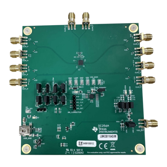
EVM User's Guide: LMKDB1104EVM
LMKDB1104 Evaluation Module
Description
The LMKDB1104 Evaluation Module (EVM) is
designed to provide a quick setup to evaluate the
LMKDB1104 LP-HCSL buffer that supports PCIe Gen
1 to Gen 6. The printed circuit board (PCB) contains
several jumpers and a USB connection to enable
the LMKDB1104 with desired user programming
and setup. The evaluation module provides flexibility
for compliance testing, system prototyping, and
performance evaluation of the LMKDB1104 device.
SNAU306 – JUNE 2024
Submit Document Feedback
Features
•
PCIe Gen 1 to Gen 6 and DB2000QL compliant
buffer
•
External and USB power supply options
•
Programmability through
graphical user interface (GUI)
•
Output enable / disable through pin controls
Applications
•
High performance computing
•
Server motherboard
•
NIC/SmartNIC
•
Hardware accelerator
LMKDB1104EVM
Copyright © 2024 Texas Instruments Incorporated
Description
TICS Pro Software GUI
LMKDB1104 Evaluation Module
1
Advertisement

Related Manuals for Texas Instruments LMKDB1104EVM


Summary of Contents for Texas Instruments LMKDB1104EVM
- Page 1 LMKDB1104 device. • High performance computing • Server motherboard • NIC/SmartNIC • Hardware accelerator LMKDB1104EVM SNAU306 – JUNE 2024 LMKDB1104 Evaluation Module Submit Document Feedback Copyright © 2024 Texas Instruments Incorporated...
- Page 2 3-wire or 4-wire SBI and SMBus interface. The EVM has integrated LDOs for excellent power supply noise suppression with operating supply voltage of 3.3V. LMKDB1104 Evaluation Module SNAU306 – JUNE 2024 Submit Document Feedback Copyright © 2024 Texas Instruments Incorporated...
- Page 3 SLEWRATE_SEL pin pulled low by default. 2.1 Hardware Setup Figure 1-1 shows default jumper configuration for the EVM. To begin using the LMKDB1104EVM, follow the steps below. 1. Verify the EVM default jumper as described in Table 2-1 Figure 1-1.
- Page 4 EVM Quick Start www.ti.com Figure 2-1. USB LED Figure 2-2. Communication Setup LMKDB1104 Evaluation Module SNAU306 – JUNE 2024 Submit Document Feedback Copyright © 2024 Texas Instruments Incorporated...
- Page 5 SBI communication. 3.2 EVM Configuration The LMKDB1104EVM can be configured for multiple modes using on board MCU and external or USB power supply options. The following sections describes power, logic, clock input, and output interfaces on the EVM and how to configure the EVM accordingly.
- Page 6 Table 3-5. Loss of Signal Detection (LOS) LOSb OUTPUT LEVEL (Status pin) LOS STATUS Detected High Not detected Table 3-6. SLEWRATE_SEL SLEWRATE_SEL OUTPUT SLEW RATE Low (default) Slow High Fast LMKDB1104 Evaluation Module SNAU306 – JUNE 2024 Submit Document Feedback Copyright © 2024 Texas Instruments Incorporated...
- Page 7 3. External AC Coupled Input. 4. Internal 50Ω to ground terminations. Figure 3-1. Input Interfaces Table 3-8 outlines how to setup all different interfaces supported by LMKDB1104. SNAU306 – JUNE 2024 LMKDB1104 Evaluation Module Submit Document Feedback Copyright © 2024 Texas Instruments Incorporated...
- Page 8 0V, such as spectrum analyzers and phase noise analyzers. 3.2.5 Status Outputs, LEDs and Test Points LMKDB1104EVM have status output signal from LMKDB1104, LEDs and test points to monitor signal / supply voltage on the board. Table 3-9 summarizes all the status signals / test points on the board.
- Page 9 LMKDB1104 TICS Pro GUI provides full functionality to interact with the device through SMBus, SBI, and OE pin option to interact with the device. TI recommends to use GUI interface while evaluating LMKDB1104EVM to fully utilize all the functionalities of the EVM. The GUI interface consists of User Controls and Raw Register page to write directly into each register bit or field values.
- Page 10 4.1.1.5 LOS Readback LOS Readback provide live status of loss of signal detection. 4.1.2 Device Info and EVM Setup Device Info page contains three different sections and the LMKDB1104EVM information. Figure 4-2. Device Info 4.1.2.1 Device Info This section contains following information related to device which can be read back using Read Device Info button.
- Page 11 SLEWRATE_CTRL_MODE needs to be set to 1 (SLEWRATE_CTRL_MODE = 1). The LMKDB1104 default is SLEWRATE_CTRL_MODE = 0, which sets all the outputs' slew rates through the SLEWRATE_PIN. SNAU306 – JUNE 2024 LMKDB1104 Evaluation Module Submit Document Feedback Copyright © 2024 Texas Instruments Incorporated...
- Page 12 Low and high voltage level can be set on all the pins using GUI without the need of onboard headers. By default, the LMKDB1104EVM is set to control OE pins through the header jumpers. To control the OE pins using software, remove jumper header J14, SBI_PRIMARY.
- Page 13 Figure 5-1 shows a typical phase noise performance for 156.25MHz reference clock input from the SMA100B. LMKDB1104EVM was configured in cascade mode to get these measurements, which were obtained by following these steps: 1. SMA100B → LMKDB1104EVM input. Then, LMKDB1104EVM to secondary LMKDB1104 EVM. This was done to get a fast slew rate at the input.
- Page 14 Hardware Design Files www.ti.com 6 Hardware Design Files 6.1 Schematics Figure 6-1. Power Supply (External and USB option) Figure 6-2. LMKDB1104 Device and CLKIN_P/N Reference LMKDB1104 Evaluation Module SNAU306 – JUNE 2024 Submit Document Feedback Copyright © 2024 Texas Instruments Incorporated...
- Page 15 Hardware Design Files Figure 6-3. Clock Outputs CLK0 to CLK7 Figure 6-4. Output Enable Pins (OE#) SNAU306 – JUNE 2024 LMKDB1104 Evaluation Module Submit Document Feedback Copyright © 2024 Texas Instruments Incorporated...
- Page 16 Hardware Design Files www.ti.com Figure 6-5. Logic I/O Jumpers Figure 6-6. Status LEDs, Test Points, and SMBus Clock and Data Connections LMKDB1104 Evaluation Module SNAU306 – JUNE 2024 Submit Document Feedback Copyright © 2024 Texas Instruments Incorporated...
- Page 17 Hardware Design Files Figure 6-7. USB Schematic and Buffer Used for SBI and OE Pin Control 6.2 PCB Layouts Figure 6-8. Layer Stackup SNAU306 – JUNE 2024 LMKDB1104 Evaluation Module Submit Document Feedback Copyright © 2024 Texas Instruments Incorporated...
- Page 18 Hardware Design Files www.ti.com Figure 6-9. Top Layer (CLKIN / CLKOUT Signals) Figure 6-10. Bottom Layer LMKDB1104 Evaluation Module SNAU306 – JUNE 2024 Submit Document Feedback Copyright © 2024 Texas Instruments Incorporated...
- Page 19 Hardware Design Files Figure 6-11. Signal 1 Layer Figure 6-12. PWR Layer SNAU306 – JUNE 2024 LMKDB1104 Evaluation Module Submit Document Feedback Copyright © 2024 Texas Instruments Incorporated...
- Page 20 Hardware Design Files www.ti.com Figure 6-13. GND 1 Layer Figure 6-14. GND 2 Layer LMKDB1104 Evaluation Module SNAU306 – JUNE 2024 Submit Document Feedback Copyright © 2024 Texas Instruments Incorporated...
- Page 21 CONN SMA JACK STR EDGE MNT CONN_JACK CON-SMA-EDGE-S RF Solutions Ltd. J8, J9, J10, J11, J18 Header, 2.54mm, 5x1, Gold, TH Header, 2.54mm, 5x1, TH 61300511121 Wurth Elektronik SNAU306 – JUNE 2024 LMKDB1104 Evaluation Module Submit Document Feedback Copyright © 2024 Texas Instruments Incorporated...
- Page 22 RES, 110 k, 1%, 0.25 W, 1206 1206 RC1206FR-07110KL Yageo America RES, 1.2M, 5%, 0.1 W, AEC-Q200 Grade 0, 1.2Meg 0603 CRCW06031M20JNEA Vishay-Dale 0603 LMKDB1104 Evaluation Module SNAU306 – JUNE 2024 Submit Document Feedback Copyright © 2024 Texas Instruments Incorporated...
- Page 23 Regulator, DQN0004A (X2SON-4) Crystal, 24.000MHz, 20pF, SMD Crystal, 11.4x4.3x3.8mm ECS-240-20-5PX-TR ECS Inc. C35, C39, C43 10uF CAP, CERM, 10µF, 16V,+/- 20%, X6S, 0603 0603 GRM188C81C106MA73D MuRata SNAU306 – JUNE 2024 LMKDB1104 Evaluation Module Submit Document Feedback Copyright © 2024 Texas Instruments Incorporated...
- Page 24 R1, R5 49.9 RES, 49.9, 1%, 0.063 W, 0402 0402 RC0402FR-0749R9L Yageo America RES, 100, 5%, 0.063 W, AEC-Q200 Grade 0, 0402 CRCW0402100RJNED Vishay-Dale 0402 LMKDB1104 Evaluation Module SNAU306 – JUNE 2024 Submit Document Feedback Copyright © 2024 Texas Instruments Incorporated...
- Page 25 Compliance Information 7 Compliance Information 7.1 Compliance and Certifications Refer to LMKDB1104EVM EU Declaration of Conformity (DoC). 8 Additional Information 8.1 Trademarks All trademarks are the property of their respective owners. 9 References For additional information on LMKDB1104, refer to LMKDB1xx data sheet.
- Page 26 STANDARD TERMS FOR EVALUATION MODULES Delivery: TI delivers TI evaluation boards, kits, or modules, including any accompanying demonstration software, components, and/or documentation which may be provided together or separately (collectively, an “EVM” or “EVMs”) to the User (“User”) in accordance with the terms set forth herein.
- Page 27 www.ti.com Regulatory Notices: 3.1 United States 3.1.1 Notice applicable to EVMs not FCC-Approved: FCC NOTICE: This kit is designed to allow product developers to evaluate electronic components, circuitry, or software associated with the kit to determine whether to incorporate such items in a finished product and software developers to write software applications for use with the end product.
- Page 28 www.ti.com Concernant les EVMs avec antennes détachables Conformément à la réglementation d'Industrie Canada, le présent émetteur radio peut fonctionner avec une antenne d'un type et d'un gain maximal (ou inférieur) approuvé pour l'émetteur par Industrie Canada. Dans le but de réduire les risques de brouillage radioélectrique à...
- Page 29 www.ti.com EVM Use Restrictions and Warnings: 4.1 EVMS ARE NOT FOR USE IN FUNCTIONAL SAFETY AND/OR SAFETY CRITICAL EVALUATIONS, INCLUDING BUT NOT LIMITED TO EVALUATIONS OF LIFE SUPPORT APPLICATIONS. 4.2 User must read and apply the user guide and other available documentation provided by TI regarding the EVM prior to handling or using the EVM, including without limitation any warning or restriction notices.
- Page 30 Notwithstanding the foregoing, any judgment may be enforced in any United States or foreign court, and TI may seek injunctive relief in any United States or foreign court. Mailing Address: Texas Instruments, Post Office Box 655303, Dallas, Texas 75265 Copyright © 2023, Texas Instruments Incorporated...
- Page 31 TI products. TI’s provision of these resources does not expand or otherwise alter TI’s applicable warranties or warranty disclaimers for TI products. TI objects to and rejects any additional or different terms you may have proposed. IMPORTANT NOTICE Mailing Address: Texas Instruments, Post Office Box 655303, Dallas, Texas 75265 Copyright © 2024, Texas Instruments Incorporated...
Need help?
Do you have a question about the LMKDB1104EVM and is the answer not in the manual?
Questions and answers