Table of Contents
Advertisement
Quick Links
www.ti.com
User's Guide
LMK1C1104DQF Low-Additive, Phase-Noise LVCMOS
Clock Buffer Evaluation Board
The LMK1C1104DQF is a high-performance, low additive jitter LVCMOS clock buffer with one LVCMOS input,
four LVCMOS outputs, and a global output enable pin.
This evaluation module (EVM) is designed to demonstrate the electrical performance of the LMK1C1104DQF.
Throughout this document, the acronym EVM and the phrases evaluation module and evaluation board are
synonymous with the LMK1C1104DFNEVM.
The EVM is equipped with 50-Ω SMA connectors and impedance-controlled 50-Ω microstrip transmission lines
for best performance.
SNAU268 – JUNE 2021
Submit Document Feedback
ABSTRACT
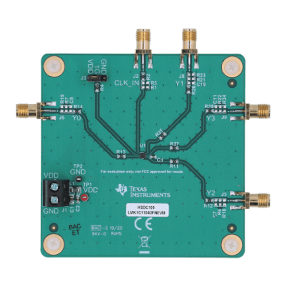
Figure 1-1. LMK1C1104DFNEVM
LMK1C1104DQF Low-Additive, Phase-Noise LVCMOS Clock Buffer
Copyright © 2021 Texas Instruments Incorporated
1
Evaluation Board
Advertisement
Table of Contents

Related Manuals for Texas Instruments LMK1C1104DQF


Summary of Contents for Texas Instruments LMK1C1104DQF
- Page 1 Clock Buffer Evaluation Board ABSTRACT The LMK1C1104DQF is a high-performance, low additive jitter LVCMOS clock buffer with one LVCMOS input, four LVCMOS outputs, and a global output enable pin. This evaluation module (EVM) is designed to demonstrate the electrical performance of the LMK1C1104DQF.
-
Page 2: Table Of Contents
Clock output traces are length matched 2 Signal Path and Control Circuitry The LMK1C1104DFNEVM supports single-ended inputs up to 250 MHz. For more information about the LMK1C1104DQF, see the LMK1C1104 product data sheet available for download from the TI Web site (www.ti.com). 3 Getting Started The LMK1C1104DFNEVM has self-explanatory labeling and uses similar naming conventions as the LMK1C1104 product data sheet. -
Page 3: Power-Supply Connections
The LMK1C1104DFNEVM operates from a single 3.3-V / 2.5-V / 1.8-V supply. 5 Enabling/Disabling the Outputs The enable pin, 1G, of the LMK1C1104DQF can be controlled using jumper J3. Pull 1G to VDD by shunting pins 2 and 3 of J3 to enable the outputs as shown in Figure 5-1. -
Page 4: Output Clock
6 Output Clock The LMK1C1104DQF fans out four LVCMOS outputs. The outputs can be loaded using the pullup and pulldown footprints. No resistor has been soldered in those footprints. The EVM board supports up to eight clock outputs for pin-compatible WSON packaged devices in the industry standard footprint. -
Page 5: Schematic
Schematic 8 Schematic Figure 8-1. LMK1C1104DFNEVM Schematic SNAU268 – JUNE 2021 LMK1C1104DQF Low-Additive, Phase-Noise LVCMOS Clock Buffer Evaluation Board Submit Document Feedback Copyright © 2021 Texas Instruments Incorporated... - Page 6 STANDARD TERMS FOR EVALUATION MODULES Delivery: TI delivers TI evaluation boards, kits, or modules, including any accompanying demonstration software, components, and/or documentation which may be provided together or separately (collectively, an “EVM” or “EVMs”) to the User (“User”) in accordance with the terms set forth herein.
- Page 7 www.ti.com Regulatory Notices: 3.1 United States 3.1.1 Notice applicable to EVMs not FCC-Approved: FCC NOTICE: This kit is designed to allow product developers to evaluate electronic components, circuitry, or software associated with the kit to determine whether to incorporate such items in a finished product and software developers to write software applications for use with the end product.
- Page 8 www.ti.com Concernant les EVMs avec antennes détachables Conformément à la réglementation d'Industrie Canada, le présent émetteur radio peut fonctionner avec une antenne d'un type et d'un gain maximal (ou inférieur) approuvé pour l'émetteur par Industrie Canada. Dans le but de réduire les risques de brouillage radioélectrique à...
- Page 9 www.ti.com EVM Use Restrictions and Warnings: 4.1 EVMS ARE NOT FOR USE IN FUNCTIONAL SAFETY AND/OR SAFETY CRITICAL EVALUATIONS, INCLUDING BUT NOT LIMITED TO EVALUATIONS OF LIFE SUPPORT APPLICATIONS. 4.2 User must read and apply the user guide and other available documentation provided by TI regarding the EVM prior to handling or using the EVM, including without limitation any warning or restriction notices.
- Page 10 Notwithstanding the foregoing, any judgment may be enforced in any United States or foreign court, and TI may seek injunctive relief in any United States or foreign court. Mailing Address: Texas Instruments, Post Office Box 655303, Dallas, Texas 75265 Copyright © 2019, Texas Instruments Incorporated...
- Page 11 TI products. TI’s provision of these resources does not expand or otherwise alter TI’s applicable warranties or warranty disclaimers for TI products.IMPORTANT NOTICE Mailing Address: Texas Instruments, Post Office Box 655303, Dallas, Texas 75265 Copyright © 2021, Texas Instruments Incorporated...
Need help?
Do you have a question about the LMK1C1104DQF and is the answer not in the manual?
Questions and answers